logo

Electrical And Electronics Engineering Fundamentals

20 Pages1774 Words40 Views
   

Added on  2022-08-08

About This Document

Hello, I need a different expert to write it in order to design the paper differently. We need to avoid plagiarism as much as we can.

Electrical And Electronics Engineering Fundamentals

   Added on 2022-08-08

ShareRelated Documents
EEE Fundamentals 1
ELECTRICAL AND ELECTRONIC ENGINEERING FUNDAMENTALS
by (Name)
Course Name
Professor (Tutor) Name
Name of University/College
City and State
Date
Electrical And Electronics Engineering Fundamentals_1
EEE Fundamentals 2
PART A
PN-Junction
P-type and N-type materials are made by adding donor and acceptor impurities respectively to a
pure silicon atom in a process known as doping. When an n-type and a p-type materials are
joined together, a pn-junction is formed and there exists a large charge density gradient between
the p and n sides (Electronics Hub 2020). Free electrons start to migrate across the pn-junction
from the n-layer (with donor impurity atoms) to the p-layer (with acceptor impurity atoms). This
diffusion process continues until a state of equilibrium is reached at the junction and the acceptor
atoms start to repel electrons while donor atoms repel the holes thus forming a potential barrier
zone across the junction (ElProCus 2020). This is called depletion region and it inhibits electron
transfer unless a forward bias voltage is applied on the pn-junction.
When a positive voltage larger than the barrier potential (0.7 V for silicon) is applied between
the p and n terminals, the potential barrier is broken and the depletion layer disappears (Lee,
Gipp. and Heller 2014). The free charges start to flow across the pn-junction and a large current
can be observed experimentally.
A diode is a pn-junction. When a voltage higher than the barrier’s potential is applied across the
diode with the negative terminal connected to n-layer and positive terminal to p-layer, electrons
in the n-type material are repelled from the negative terminal since they are like charges. The
electrons cross the potential barrier to cling on the holes in the p-layer. Due to the attraction by
the positive terminal, these electrons jump to the next holes towards the positive terminal and
eventually flow through the external circuit. The diode is said to be forward-biased allowing
current flow through it (ElProCus 2020).
Electrical And Electronics Engineering Fundamentals_2
EEE Fundamentals 3
However, applying voltage across the diode with the negative terminal of the battery connected
to the p-layer and positive terminal of the battery to the n-layer, the holes and electrons in both
regions will be attracted by the power source (ElProCus 2020). This increases the width of the
depletion region and flow of charge is impossible. The diode is said to be reverse-biased.
PART B: Voltage discharging curve across a capacitor in RC network
The RC time constant; τ =340 μs
Using a capacitor value of 1 μF
Consider, τ =RC (RC circuits 2020).
Resistor value to achieve τ =340 μs is given by: R= τ
C =340 ×106
1 ×106 =340 Ω
Electrical And Electronics Engineering Fundamentals_3
EEE Fundamentals 4
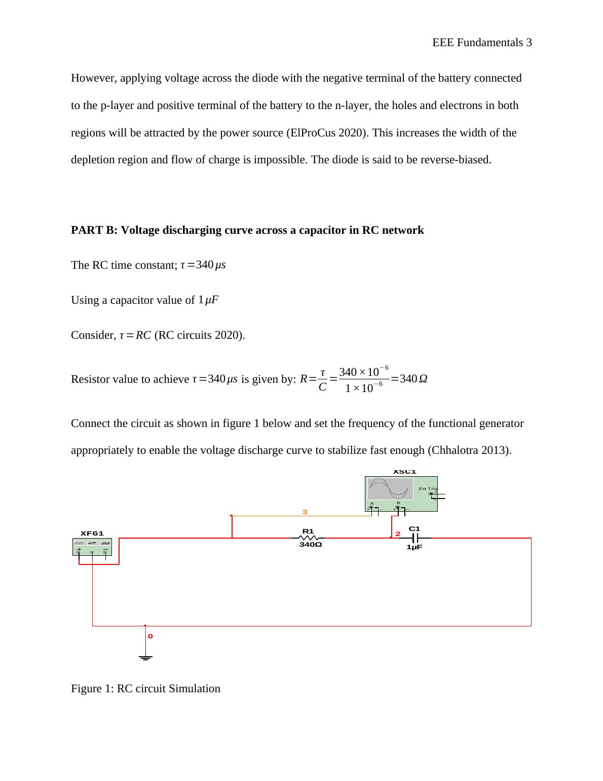
Connect the circuit as shown in figure 1 below and set the frequency of the functional generator
appropriately to enable the voltage discharge curve to stabilize fast enough (Chhalotra 2013).
R1
340Ω
C1
1μF
XFG1
XSC1
A B
Ext Trig
+
+
_
_ + _
0
2
3
Figure 1: RC circuit Simulation
Electrical And Electronics Engineering Fundamentals_4

End of preview

Want to access all the pages? Upload your documents or become a member.

Related Documents
Desklib - Online Library for Study Material with Solved Assignments, Essays, Dissertations
|25
|2177
|288

Basic Electrical Principles: Circuits, Capacitors, Diodes, Magnetic Fields, and Transformers
|21
|2944
|314

Analogue Electronics Circuits
|20
|3349
|44

Analogue Electronic Circuits
|20
|3810
|98