Electronics Assignment: Analysis of Digital and Analog Systems
VerifiedAdded on 2022/08/26
|14
|1481
|16
Homework Assignment
AI Summary
This electronics assignment solution provides a detailed analysis of various concepts in electrical engineering. The assignment covers topics including minimum bandwidth calculations, DAC (Digital-to-Analog Converter) analysis for 8-bit and 12-bit systems, and the advantages and disadvantages of different DAC bit resolutions. It further explores Fast Ethernet LAN standards, synchronous and asynchronous data transfer methods, and the operation and applications of semiconductor laser sources, comparing them with LEDs. The assignment also delves into nonlinear quantization with PCM (Pulse Code Modulation), discussing A-law and µ-law companding techniques, quantization noise, and signal-to-noise ratio calculations. The solution includes detailed explanations, formulas, and calculations related to each topic, providing a comprehensive understanding of the underlying principles.

Electronics 1
ELECTRONICS
by (Name)
Course Name
Professor (Tutor) Name
Name of University/College
City and State
Date
ELECTRONICS
by (Name)
Course Name
Professor (Tutor) Name
Name of University/College
City and State
Date
Paraphrase This Document
Need a fresh take? Get an instant paraphrase of this document with our AI Paraphraser
Electronics 2
Question 1
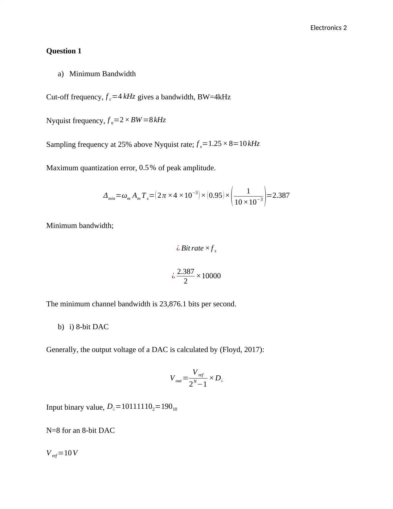
a) Minimum Bandwidth
Cut-off frequency, f c=4 kHz gives a bandwidth, BW=4kHz
Nyquist frequency, f n=2 × BW =8 kHz
Sampling frequency at 25% above Nyquist rate; f s=1.25 × 8=10 kHz
Maximum quantization error, 0.5 % of peak amplitude.
Δmin=ωm Am T s= ( 2 π ×4 ×10−3 ) × ( 0.95 ) × ( 1
10 ×10−3 )=2.387
Minimum bandwidth;
¿ Bit rate × f s
¿ 2.387
2 ×10000
The minimum channel bandwidth is 23,876.1 bits per second.
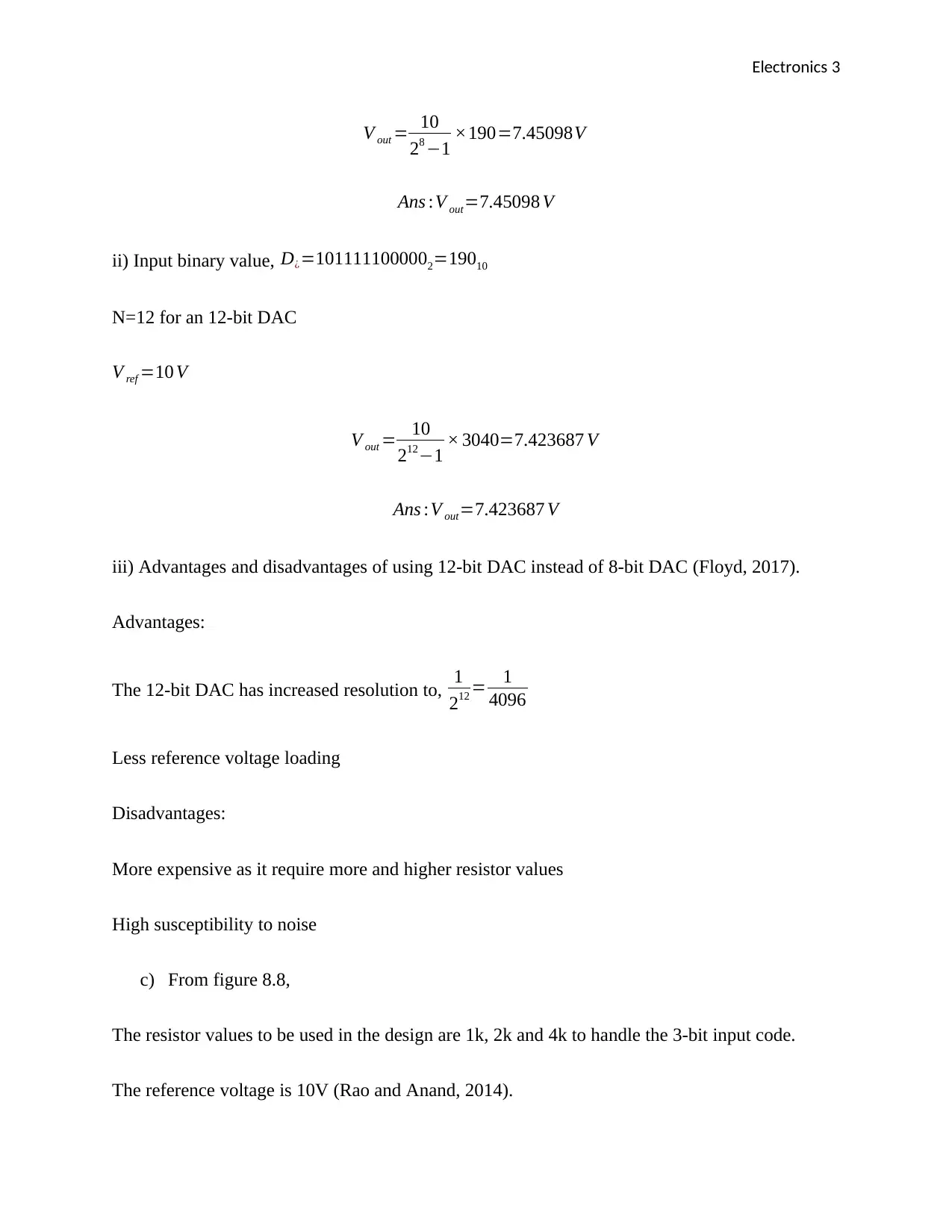
b) i) 8-bit DAC
Generally, the output voltage of a DAC is calculated by (Floyd, 2017):
V out = V ref
2N−1 × D¿
Input binary value, D¿=101111102=19010
N=8 for an 8-bit DAC
V ref =10 V
Electronics 3
V out = 10
28 −1 ×190=7.45098V
Ans :V out=7.45098 V
ii) Input binary value, D¿=1011111000002=19010
N=12 for an 12-bit DAC
V ref =10 V
V out = 10
212−1 × 3040=7.423687 V
Ans :V out=7.423687 V
iii) Advantages and disadvantages of using 12-bit DAC instead of 8-bit DAC (Floyd, 2017).
Advantages:
The 12-bit DAC has increased resolution to, 1
212 = 1
4096
Less reference voltage loading
Disadvantages:
More expensive as it require more and higher resistor values
High susceptibility to noise
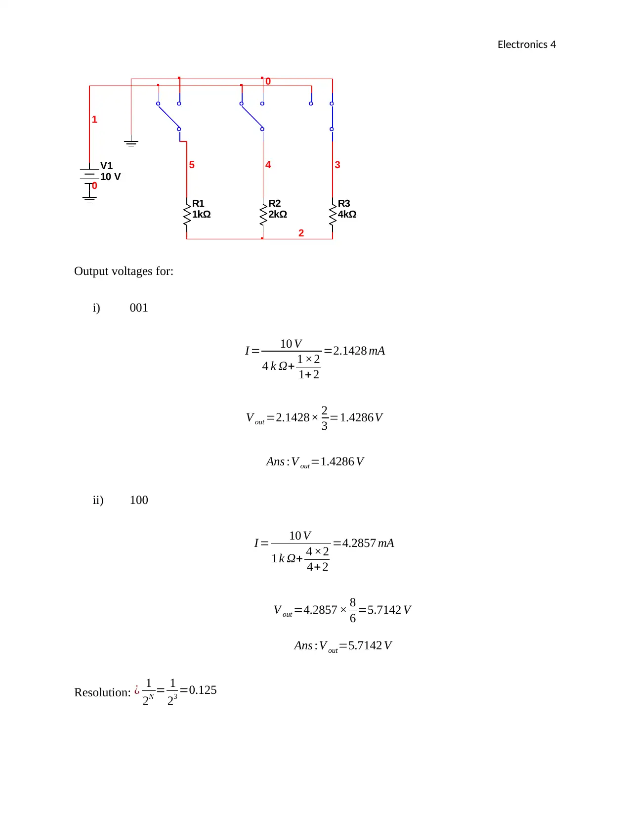
c) From figure 8.8,
The resistor values to be used in the design are 1k, 2k and 4k to handle the 3-bit input code.
The reference voltage is 10V (Rao and Anand, 2014).
V out = 10
28 −1 ×190=7.45098V
Ans :V out=7.45098 V
ii) Input binary value, D¿=1011111000002=19010
N=12 for an 12-bit DAC
V ref =10 V
V out = 10
212−1 × 3040=7.423687 V
Ans :V out=7.423687 V
iii) Advantages and disadvantages of using 12-bit DAC instead of 8-bit DAC (Floyd, 2017).
Advantages:
The 12-bit DAC has increased resolution to, 1
212 = 1
4096
Less reference voltage loading
Disadvantages:
More expensive as it require more and higher resistor values
High susceptibility to noise
c) From figure 8.8,
The resistor values to be used in the design are 1k, 2k and 4k to handle the 3-bit input code.
The reference voltage is 10V (Rao and Anand, 2014).
⊘ This is a preview!⊘
Do you want full access?
Subscribe today to unlock all pages.

Trusted by 1+ million students worldwide
Electronics 4
R1
1kΩ
R2
2kΩ
R3
4kΩ
V1
10 V
0
2
345
1
0
Output voltages for:
i) 001
I = 10 V
4 k Ω+ 1 ×2
1+ 2
=2.1428 mA
V out =2.1428× 2
3 =1.4286V
Ans :V out=1.4286 V
ii) 100
I = 10 V
1 k Ω+ 4 ×2
4+ 2
=4.2857 mA
V out =4.2857 × 8
6 =5.7142 V
Ans :V out=5.7142 V
Resolution: ¿ 1
2N = 1
23 =0.125
R1
1kΩ
R2
2kΩ
R3
4kΩ
V1
10 V
0
2
345
1
0
Output voltages for:
i) 001
I = 10 V
4 k Ω+ 1 ×2
1+ 2
=2.1428 mA
V out =2.1428× 2
3 =1.4286V
Ans :V out=1.4286 V
ii) 100
I = 10 V
1 k Ω+ 4 ×2
4+ 2
=4.2857 mA
V out =4.2857 × 8
6 =5.7142 V
Ans :V out=5.7142 V
Resolution: ¿ 1
2N = 1
23 =0.125
Paraphrase This Document
Need a fresh take? Get an instant paraphrase of this document with our AI Paraphraser
Electronics 5
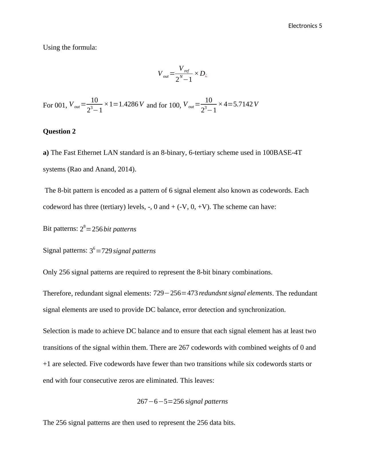
Using the formula:
V out = V ref
2N−1 × D¿
For 001, V out = 10
23−1 ×1=1.4286 V and for 100, V out = 10
23−1 × 4=5.7142 V
Question 2
a) The Fast Ethernet LAN standard is an 8-binary, 6-tertiary scheme used in 100BASE-4T
systems (Rao and Anand, 2014).
The 8-bit pattern is encoded as a pattern of 6 signal element also known as codewords. Each
codeword has three (tertiary) levels, -, 0 and + (-V, 0, +V). The scheme can have:
Bit patterns: 28=256 bit patterns
Signal patterns: 36 =729 signal patterns
Only 256 signal patterns are required to represent the 8-bit binary combinations.
Therefore, redundant signal elements: 729−256=473 redundsnt signal elements. The redundant
signal elements are used to provide DC balance, error detection and synchronization.
Selection is made to achieve DC balance and to ensure that each signal element has at least two
transitions of the signal within them. There are 267 codewords with combined weights of 0 and
+1 are selected. Five codewords have fewer than two transitions while six codewords starts or
end with four consecutive zeros are eliminated. This leaves:
267−6−5=256 signal patterns
The 256 signal patterns are then used to represent the 256 data bits.
Electronics 6
For Dc balance, two groups of +1 weights cannot follow each other in succession since it will
cause interpretation of the signal at receiver end. This DC Wander is eliminated by writing the
first signal-pattern the way it is and inverting the next signal pattern to have -1 weight which will
be interpreted by the receiver as inverted signal (Floyd, 2017).
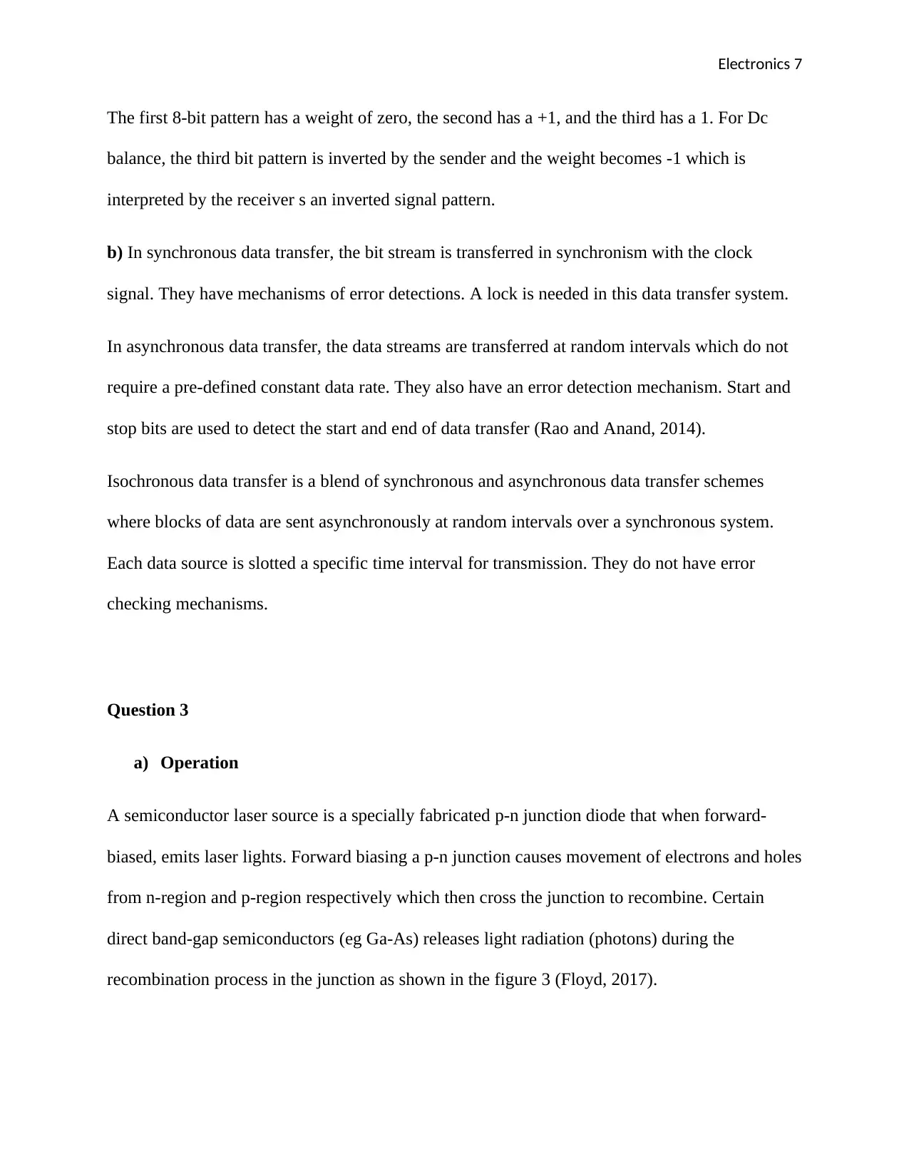
For example, the figure below shows the encoding of a three 8-bit data pattern as three 6-tertiary
signal patterns. To convert a binary bit to ternary signal, the following table is used (Rao and
Anand, 2014).
Binary Ternary
00 -
01 0
10 0
11 +
⊘ This is a preview!⊘
Do you want full access?
Subscribe today to unlock all pages.

Trusted by 1+ million students worldwide
Electronics 7
The first 8-bit pattern has a weight of zero, the second has a +1, and the third has a 1. For Dc
balance, the third bit pattern is inverted by the sender and the weight becomes -1 which is
interpreted by the receiver s an inverted signal pattern.
b) In synchronous data transfer, the bit stream is transferred in synchronism with the clock
signal. They have mechanisms of error detections. A lock is needed in this data transfer system.
In asynchronous data transfer, the data streams are transferred at random intervals which do not
require a pre-defined constant data rate. They also have an error detection mechanism. Start and
stop bits are used to detect the start and end of data transfer (Rao and Anand, 2014).
Isochronous data transfer is a blend of synchronous and asynchronous data transfer schemes
where blocks of data are sent asynchronously at random intervals over a synchronous system.
Each data source is slotted a specific time interval for transmission. They do not have error
checking mechanisms.
Question 3
a) Operation
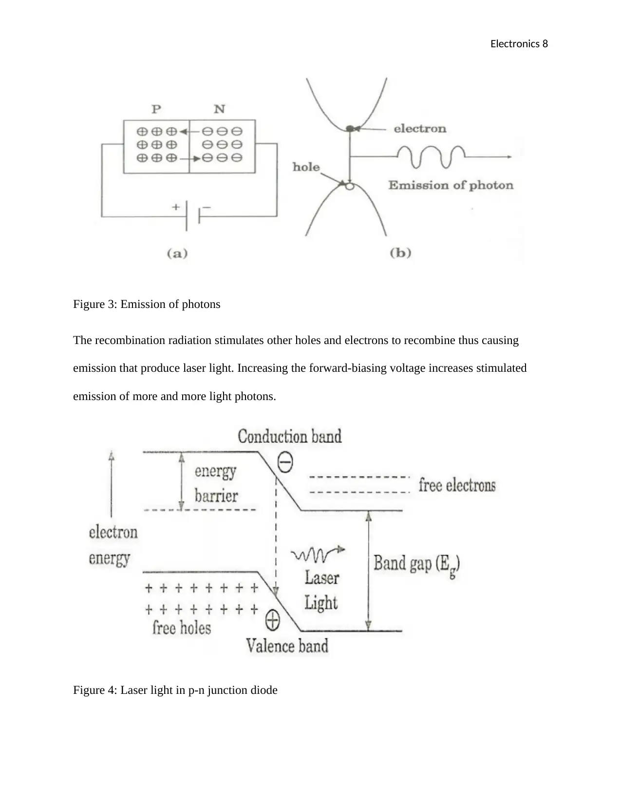
A semiconductor laser source is a specially fabricated p-n junction diode that when forward-
biased, emits laser lights. Forward biasing a p-n junction causes movement of electrons and holes
from n-region and p-region respectively which then cross the junction to recombine. Certain
direct band-gap semiconductors (eg Ga-As) releases light radiation (photons) during the
recombination process in the junction as shown in the figure 3 (Floyd, 2017).
Paraphrase This Document
Need a fresh take? Get an instant paraphrase of this document with our AI Paraphraser
Electronics 8
Figure 3: Emission of photons
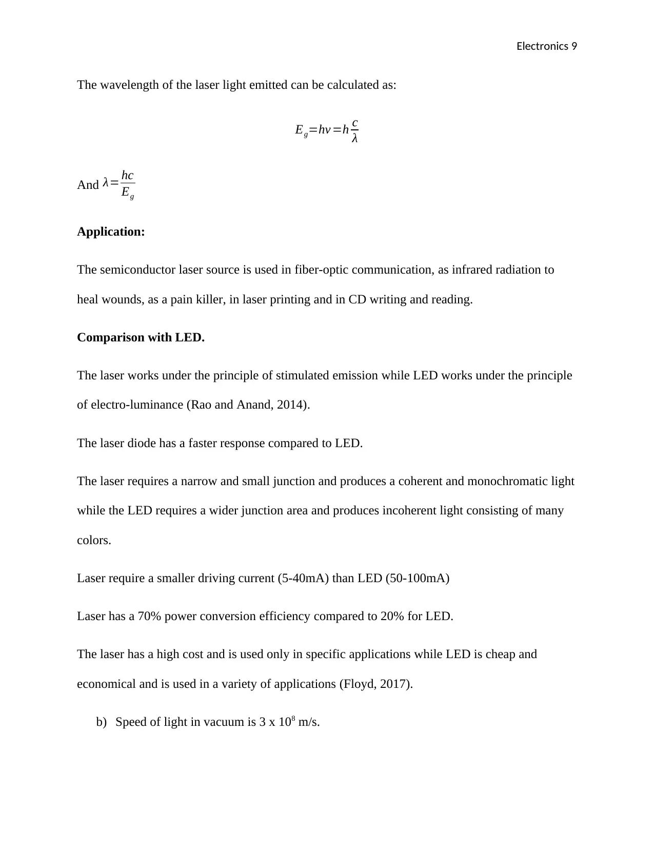
The recombination radiation stimulates other holes and electrons to recombine thus causing
emission that produce laser light. Increasing the forward-biasing voltage increases stimulated
emission of more and more light photons.
Figure 4: Laser light in p-n junction diode
Electronics 9
The wavelength of the laser light emitted can be calculated as:
Eg=hv =h c
λ
And λ= hc
Eg
Application:
The semiconductor laser source is used in fiber-optic communication, as infrared radiation to
heal wounds, as a pain killer, in laser printing and in CD writing and reading.
Comparison with LED.
The laser works under the principle of stimulated emission while LED works under the principle
of electro-luminance (Rao and Anand, 2014).
The laser diode has a faster response compared to LED.
The laser requires a narrow and small junction and produces a coherent and monochromatic light
while the LED requires a wider junction area and produces incoherent light consisting of many
colors.
Laser require a smaller driving current (5-40mA) than LED (50-100mA)
Laser has a 70% power conversion efficiency compared to 20% for LED.
The laser has a high cost and is used only in specific applications while LED is cheap and
economical and is used in a variety of applications (Floyd, 2017).
b) Speed of light in vacuum is 3 x 10⁸ m/s.
⊘ This is a preview!⊘
Do you want full access?
Subscribe today to unlock all pages.

Trusted by 1+ million students worldwide
Electronics 10
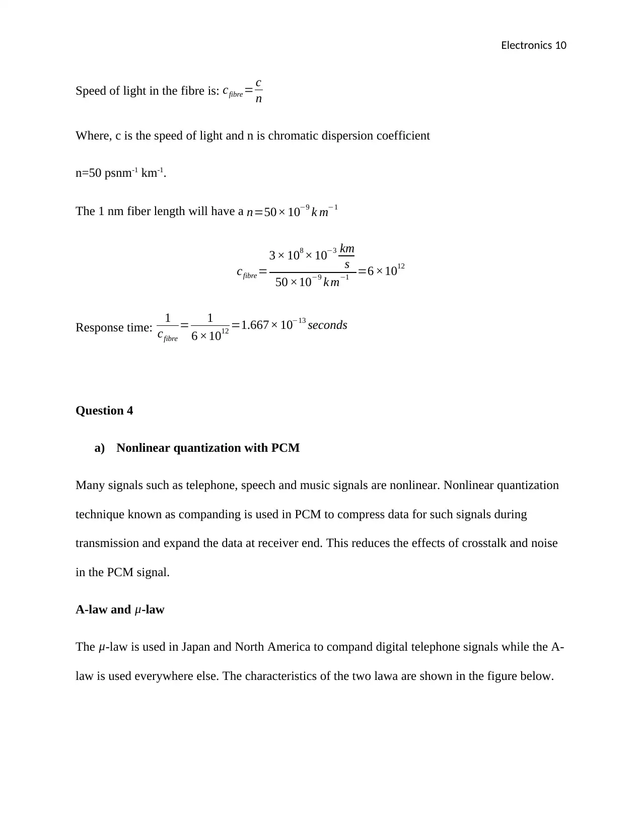
Speed of light in the fibre is: cfibre = c
n
Where, c is the speed of light and n is chromatic dispersion coefficient
n=50 psnm-1 km-1.
The 1 nm fiber length will have a n=50× 10−9 k m−1
cfibre =
3 × 108 × 10−3 km
s
50 ×10−9 k m−1 =6 ×10¹²
Response time: 1
cfibre
= 1
6 ×1012 =1.667× 10⁻¹³ seconds
Question 4
a) Nonlinear quantization with PCM
Many signals such as telephone, speech and music signals are nonlinear. Nonlinear quantization
technique known as companding is used in PCM to compress data for such signals during
transmission and expand the data at receiver end. This reduces the effects of crosstalk and noise
in the PCM signal.
A-law and μ-law
The μ-law is used in Japan and North America to compand digital telephone signals while the A-
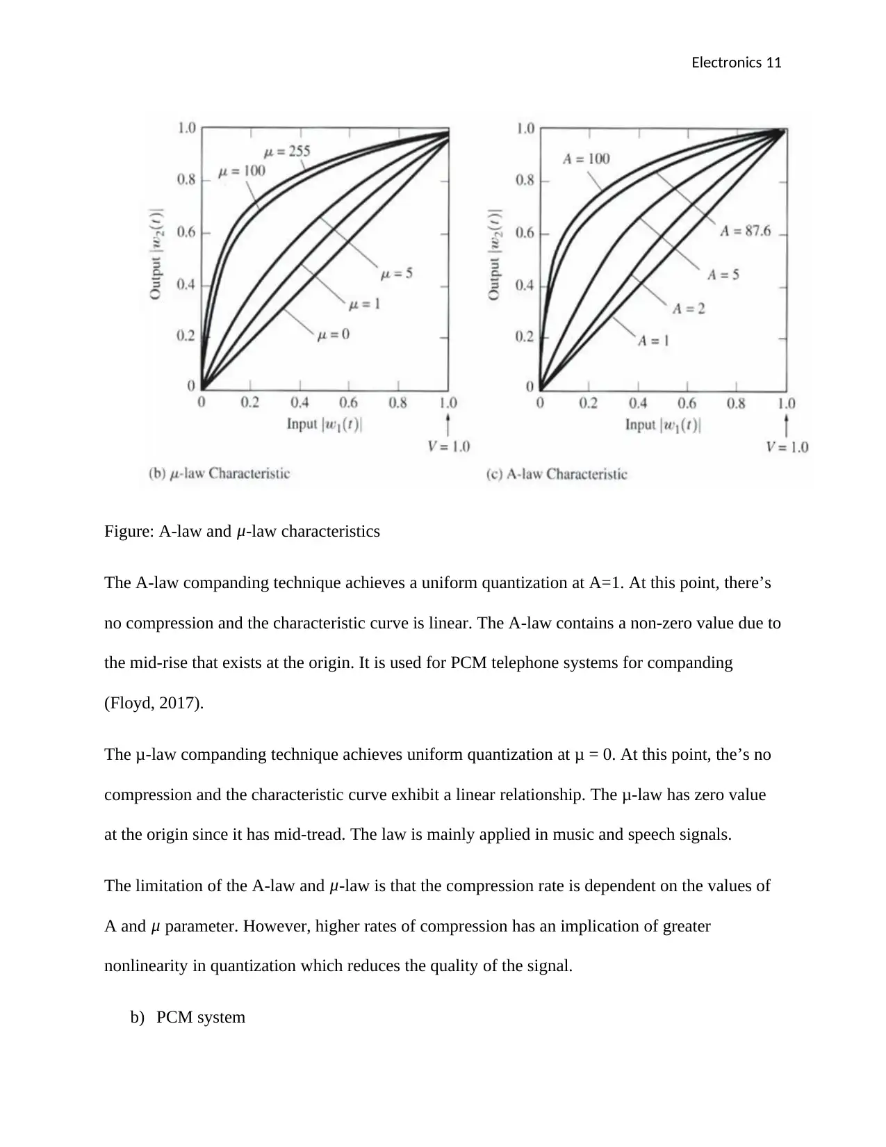
law is used everywhere else. The characteristics of the two lawa are shown in the figure below.
Paraphrase This Document
Need a fresh take? Get an instant paraphrase of this document with our AI Paraphraser
Electronics 11
Figure: A-law and μ-law characteristics
The A-law companding technique achieves a uniform quantization at A=1. At this point, there’s
no compression and the characteristic curve is linear. The A-law contains a non-zero value due to
the mid-rise that exists at the origin. It is used for PCM telephone systems for companding
(Floyd, 2017).
The μ-law companding technique achieves uniform quantization at μ = 0. At this point, the’s no
compression and the characteristic curve exhibit a linear relationship. The μ-law has zero value
at the origin since it has mid-tread. The law is mainly applied in music and speech signals.
The limitation of the A-law and μ-law is that the compression rate is dependent on the values of
A and μ parameter. However, higher rates of compression has an implication of greater
nonlinearity in quantization which reduces the quality of the signal.
b) PCM system
Electronics 12
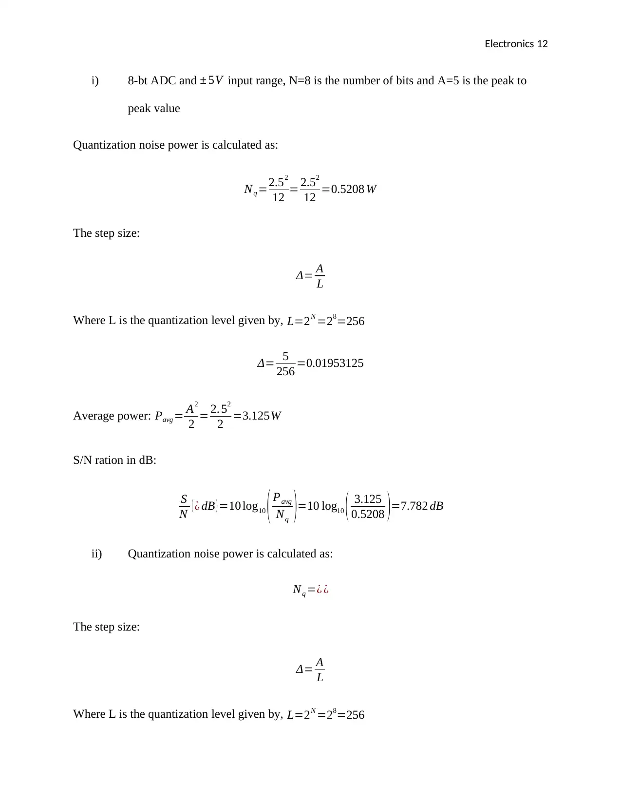
i) 8-bt ADC and ± 5V input range, N=8 is the number of bits and A=5 is the peak to
peak value
Quantization noise power is calculated as:
Nq =2.52
12 = 2.52
12 =0.5208 W
The step size:
Δ= A
L
Where L is the quantization level given by, L=2N =28=256
Δ= 5
256 =0.01953125
Average power: Pavg = A2
2 = 2. 52
2 =3.125W
S/N ration in dB:
S
N ( ¿ dB ) =10 log10 ( Pavg
Nq )=10 log10 ( 3.125
0.5208 )=7.782 dB
ii) Quantization noise power is calculated as:
Nq =¿ ¿
The step size:
Δ= A
L
Where L is the quantization level given by, L=2N =28=256
⊘ This is a preview!⊘
Do you want full access?
Subscribe today to unlock all pages.

Trusted by 1+ million students worldwide
1 out of 14
Your All-in-One AI-Powered Toolkit for Academic Success.
+13062052269
info@desklib.com
Available 24*7 on WhatsApp / Email
![[object Object]](/_next/static/media/star-bottom.7253800d.svg)
Unlock your academic potential
Copyright © 2020–2025 A2Z Services. All Rights Reserved. Developed and managed by ZUCOL.