Analog Electronics 3 Home Assignment: Circuit Analysis and Design
VerifiedAdded on 2023/06/16
|13
|2168
|96
AI Summary
This home assignment covers network analysis techniques, op-amp circuit analysis, analog circuit design, and evaluation. It includes questions on threshold detector current source, voltage controlled current source, and circuit calibration. The assignment also covers the choice of appropriate components and circuit construction on Proteus.
Contribute Materials
Your contribution can guide someone’s learning journey. Share your
documents today.

UNIVERSITY AFFILIATION
DEPARTMENT OR FACULTY
COURSE NAME
COURSE CODE
STUDENT NAME
STUDENT REGISTRATION ID
DATE OF SUBMISSION
1
DEPARTMENT OR FACULTY
COURSE NAME
COURSE CODE
STUDENT NAME
STUDENT REGISTRATION ID
DATE OF SUBMISSION
1
Secure Best Marks with AI Grader
Need help grading? Try our AI Grader for instant feedback on your assignments.
ANALOGUE ELECTRONICS 3 - HOME ASSIGNMENT
OBECTIVES
(i) Use network analysis techniques to analyze a circuit
(ii) Analyze an op-amp circuit to determine its transfer function
(iii) Choose a suitable op-amp for an application
(iv) Design and test an analog circuit as a solution to an engineering situation
(v) Evaluate the design of an analog circuit with respect to a set of specifications
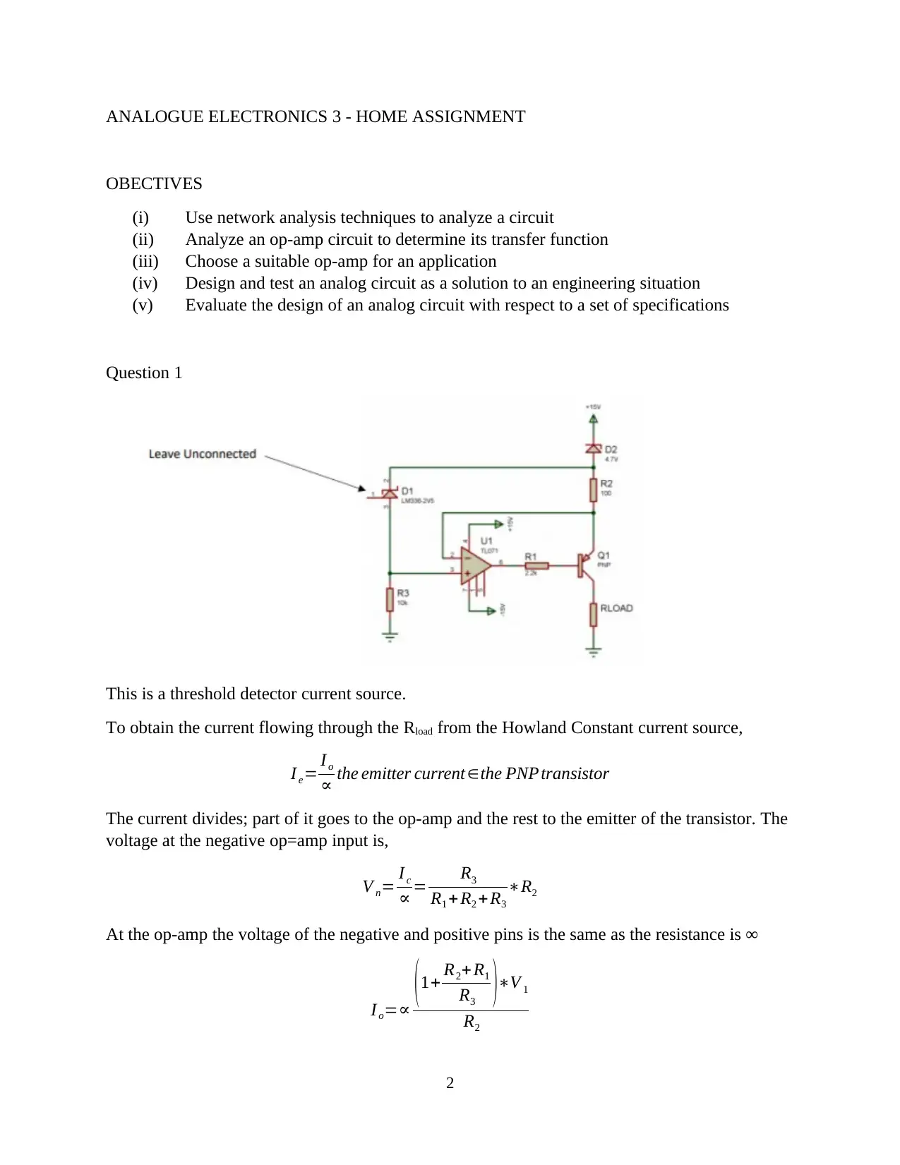
Question 1
This is a threshold detector current source.
To obtain the current flowing through the Rload from the Howland Constant current source,
I e= Io
∝ the emitter current ∈the PNP transistor
The current divides; part of it goes to the op-amp and the rest to the emitter of the transistor. The
voltage at the negative op=amp input is,
V n= I c
∝ = R3
R1 + R2 + R3
∗R2
At the op-amp the voltage of the negative and positive pins is the same as the resistance is ∞
I o=∝
(1+ R2+ R1
R3 )∗V 1
R2
2
OBECTIVES
(i) Use network analysis techniques to analyze a circuit
(ii) Analyze an op-amp circuit to determine its transfer function
(iii) Choose a suitable op-amp for an application
(iv) Design and test an analog circuit as a solution to an engineering situation
(v) Evaluate the design of an analog circuit with respect to a set of specifications
Question 1
This is a threshold detector current source.
To obtain the current flowing through the Rload from the Howland Constant current source,
I e= Io
∝ the emitter current ∈the PNP transistor
The current divides; part of it goes to the op-amp and the rest to the emitter of the transistor. The
voltage at the negative op=amp input is,
V n= I c
∝ = R3
R1 + R2 + R3
∗R2
At the op-amp the voltage of the negative and positive pins is the same as the resistance is ∞
I o=∝
(1+ R2+ R1
R3 )∗V 1
R2
2
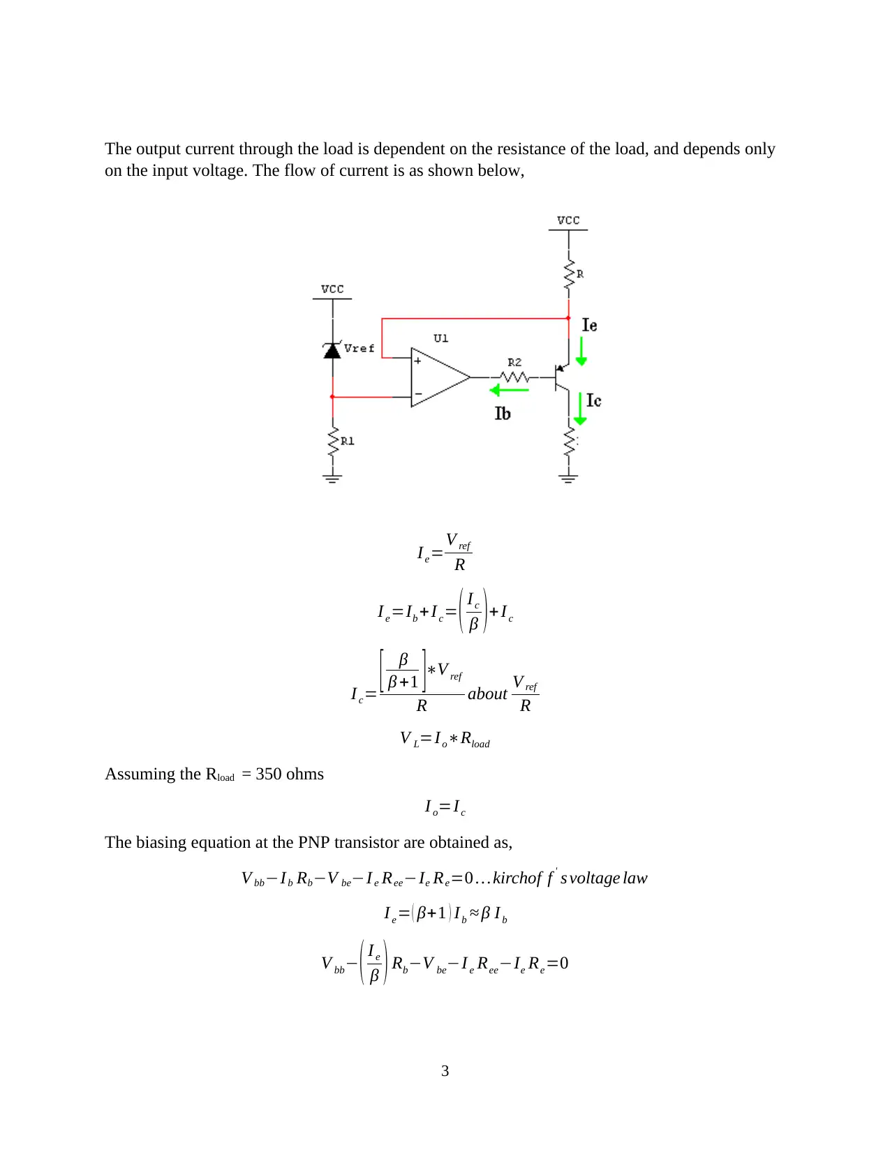
The output current through the load is dependent on the resistance of the load, and depends only
on the input voltage. The flow of current is as shown below,
Ie=V ref
R
I e=Ib +Ic= ( Ic
β )+ Ic
I c= [ β
β +1 ]∗V ref
R about V ref
R
V L=Io∗Rload
Assuming the Rload = 350 ohms
I o=I c
The biasing equation at the PNP transistor are obtained as,
V bb−Ib Rb−V be−I e Ree−Ie Re=0 … kirchof f ' s voltage law
I e= ( β+1 ) I b ≈ β I b
V bb− ( I e
β ) Rb−V be−I e Ree−Ie Re=0
3
V bb−V be= (I e ( Rb
β )+ I e Ree+I e Re )
I e= V bb−V be
Rb
β + Ree + Re
Rb
β + Ree+ Re=V bb−V be
Ie
Rb =β [ V bb−V be
Ie
− ( Ree + Re ) ]
Using actual values,
Rb =β [ 15−0.7
Ie
− ( 100+0.5 ) ]
Assuming that the gain is 100 and Vbe is 0.7V,
2.2 k=100 [ 15−0.7
Ie
− ( 100+0.5 ) ]
The emitter current is given as,
I e= 15−0.7
2200
100 + 0.5+100
I e= 14.3
122.5 =0.116735 Amps
I e ≈ 120 mA rating
The emitter bias with internal emitter resistance included results in the equation,
Ree= 26 mV
I e
Where Rb is R1 , Re is R3 while the Ree is the PNP internal resistance at the emitter section
The current flowing through the emitter is said to be the same as that at the collector or a bit
amplified due to the presence of the op-amp. Therefore,
I e ≈ Ic
The value of the gain factor determines the current flowing through the load.
To obtain the voltage across the load,
4
Secure Best Marks with AI Grader
Need help grading? Try our AI Grader for instant feedback on your assignments.
V L=120 mA∗340 Ω
V L=40.8 V … at the collector
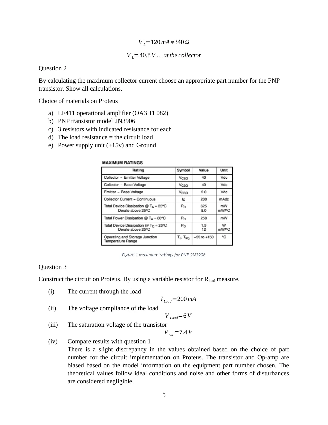
Question 2
By calculating the maximum collector current choose an appropriate part number for the PNP
transistor. Show all calculations.
Choice of materials on Proteus
a) LF411 operational amplifier (OA3 TL082)
b) PNP transistor model 2N3906
c) 3 resistors with indicated resistance for each
d) The load resistance = the circuit load
e) Power supply unit (+15v) and Ground
Figure 1 maximum ratings for PNP 2N3906
Question 3
Construct the circuit on Proteus. By using a variable resistor for Rload measure,
(i) The current through the load
I Load =200 mA
(ii) The voltage compliance of the load
V Load=6 V
(iii) The saturation voltage of the transistor
V sat =7.4 V
(iv) Compare results with question 1
There is a slight discrepancy in the values obtained based on the choice of part
number for the circuit implementation on Proteus. The transistor and Op-amp are
biased based on the model information on the equipment part number chosen. The
theoretical values follow ideal conditions and noise and other forms of disturbances
are considered negligible.
5
V L=40.8 V … at the collector
Question 2
By calculating the maximum collector current choose an appropriate part number for the PNP
transistor. Show all calculations.
Choice of materials on Proteus
a) LF411 operational amplifier (OA3 TL082)
b) PNP transistor model 2N3906
c) 3 resistors with indicated resistance for each
d) The load resistance = the circuit load
e) Power supply unit (+15v) and Ground
Figure 1 maximum ratings for PNP 2N3906
Question 3
Construct the circuit on Proteus. By using a variable resistor for Rload measure,
(i) The current through the load
I Load =200 mA
(ii) The voltage compliance of the load
V Load=6 V
(iii) The saturation voltage of the transistor
V sat =7.4 V
(iv) Compare results with question 1
There is a slight discrepancy in the values obtained based on the choice of part
number for the circuit implementation on Proteus. The transistor and Op-amp are
biased based on the model information on the equipment part number chosen. The
theoretical values follow ideal conditions and noise and other forms of disturbances
are considered negligible.
5
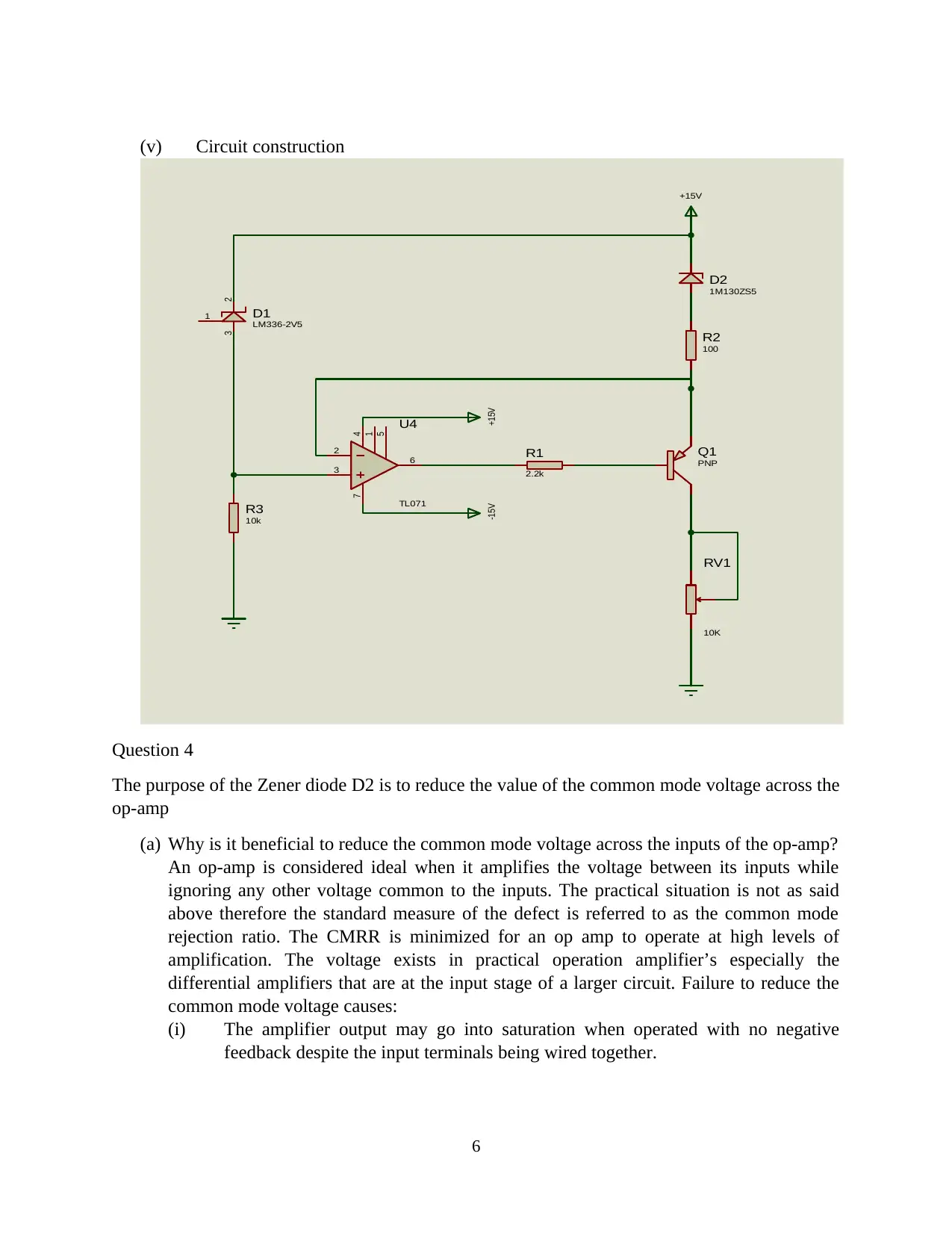
(v) Circuit construction
Q1
PNP
R1
2.2k
R2
100
D2
1M130ZS5
R3
10k
RV1
10K
23
1 D1
LM336-2V5
+15V
+15V-15V
3
2
6
7 4
1
5 U4
TL071
Question 4
The purpose of the Zener diode D2 is to reduce the value of the common mode voltage across the
op-amp
(a) Why is it beneficial to reduce the common mode voltage across the inputs of the op-amp?
An op-amp is considered ideal when it amplifies the voltage between its inputs while
ignoring any other voltage common to the inputs. The practical situation is not as said
above therefore the standard measure of the defect is referred to as the common mode
rejection ratio. The CMRR is minimized for an op amp to operate at high levels of
amplification. The voltage exists in practical operation amplifier’s especially the
differential amplifiers that are at the input stage of a larger circuit. Failure to reduce the
common mode voltage causes:
(i) The amplifier output may go into saturation when operated with no negative
feedback despite the input terminals being wired together.
6
(ii) The negative feedback configuration in a closed loop setup has the input offset
voltage amplified alongside the signal which may pose a problem when the high
precision DC amplification is required or when the input signal is small.
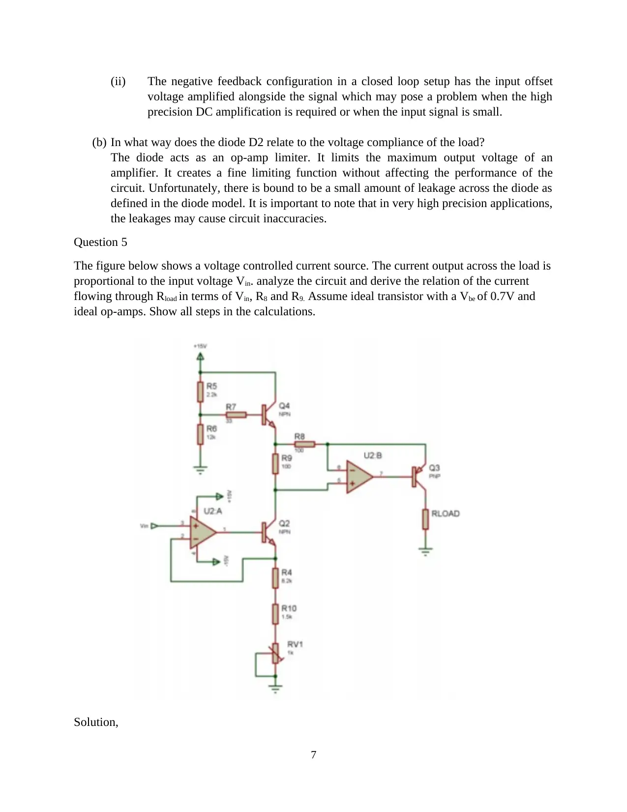
(b) In what way does the diode D2 relate to the voltage compliance of the load?
The diode acts as an op-amp limiter. It limits the maximum output voltage of an
amplifier. It creates a fine limiting function without affecting the performance of the
circuit. Unfortunately, there is bound to be a small amount of leakage across the diode as
defined in the diode model. It is important to note that in very high precision applications,
the leakages may cause circuit inaccuracies.
Question 5
The figure below shows a voltage controlled current source. The current output across the load is
proportional to the input voltage Vin. analyze the circuit and derive the relation of the current
flowing through Rload in terms of Vin, R8 and R9. Assume ideal transistor with a Vbe of 0.7V and
ideal op-amps. Show all steps in the calculations.
Solution,
7
voltage amplified alongside the signal which may pose a problem when the high
precision DC amplification is required or when the input signal is small.
(b) In what way does the diode D2 relate to the voltage compliance of the load?
The diode acts as an op-amp limiter. It limits the maximum output voltage of an
amplifier. It creates a fine limiting function without affecting the performance of the
circuit. Unfortunately, there is bound to be a small amount of leakage across the diode as
defined in the diode model. It is important to note that in very high precision applications,
the leakages may cause circuit inaccuracies.
Question 5
The figure below shows a voltage controlled current source. The current output across the load is
proportional to the input voltage Vin. analyze the circuit and derive the relation of the current
flowing through Rload in terms of Vin, R8 and R9. Assume ideal transistor with a Vbe of 0.7V and
ideal op-amps. Show all steps in the calculations.
Solution,
7
Paraphrase This Document
Need a fresh take? Get an instant paraphrase of this document with our AI Paraphraser
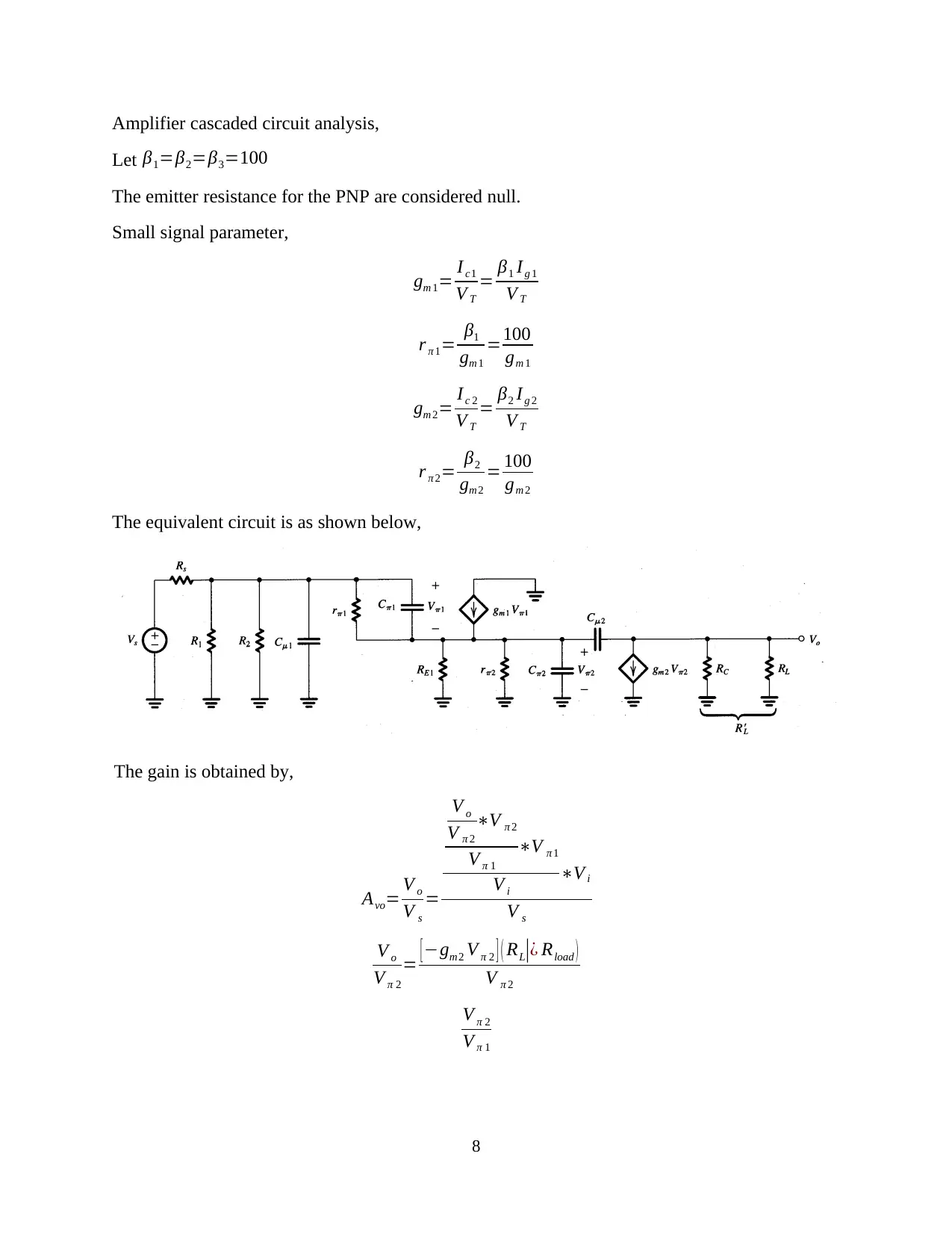
Amplifier cascaded circuit analysis,
Let β1=β2=β3=100
The emitter resistance for the PNP are considered null.
Small signal parameter,
gm 1= I c1
V T
= β1 Ig 1
V T
r π 1= β1
gm 1
=100
gm 1
gm 2= I c 2
V T
= β2 Ig 2
V T
r π 2= β2
gm 2
= 100
gm 2
The equivalent circuit is as shown below,
The gain is obtained by,
Avo= V o
V s
=
V o
V π 2
∗V π 2
V π 1
∗V π 1
V i
∗V i
V s
V o
V π 2
= [−gm2 V π 2 ] ( RL|¿ Rload )
V π 2
V π 2
V π 1
8
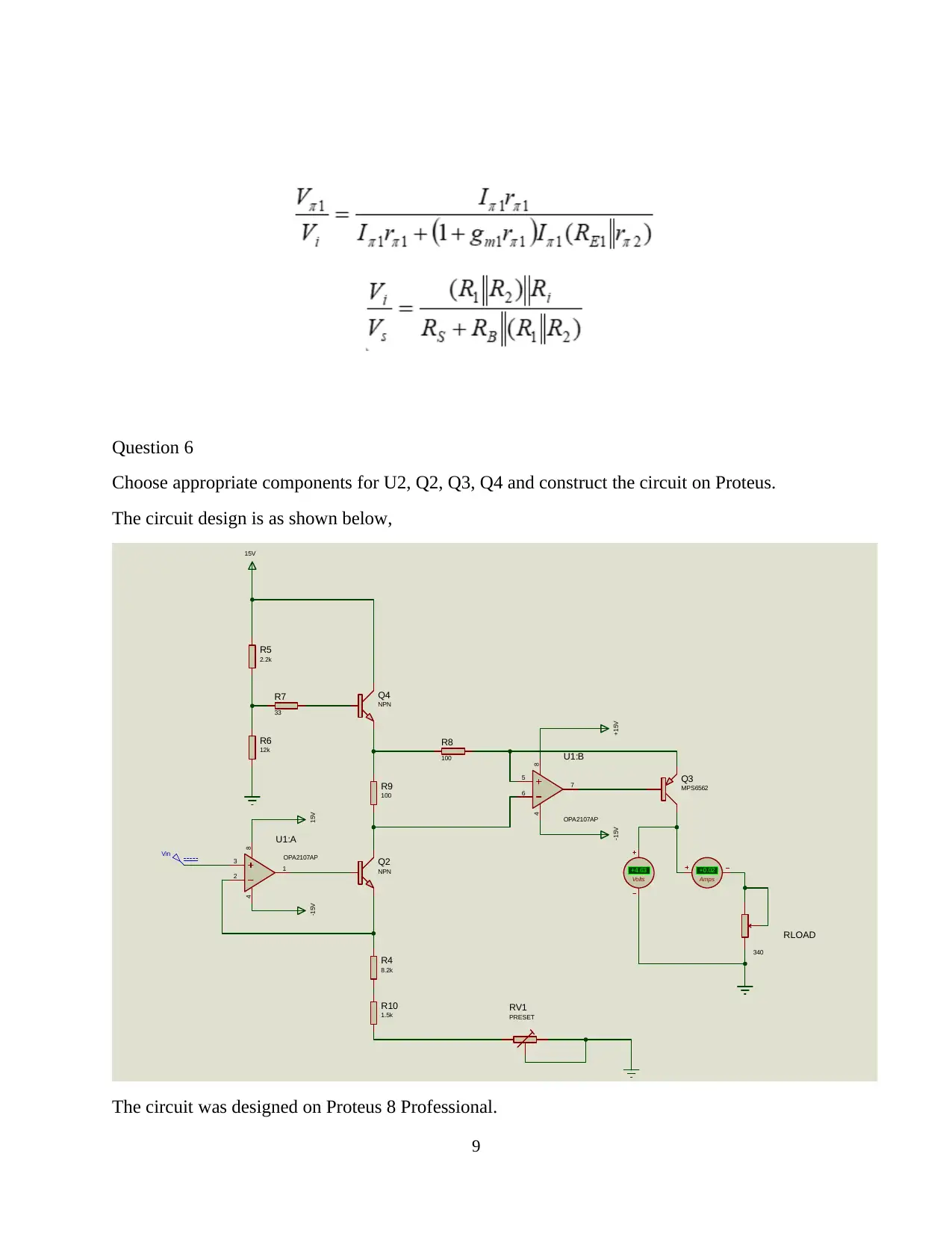
Question 6
Choose appropriate components for U2, Q2, Q3, Q4 and construct the circuit on Proteus.
The circuit design is as shown below,
R4
8.2k
R5
2.2k
R6
12k
R7
33
R8
100
R9
100
R10
1.5k
Q4
NPN
Q2
NPN
RV1
PRESET
15V
3
2
1
84
U1:A
OPA2107AP
5
6
7
84
U1:B
OPA2107AP
Q3
MPS6562
RLOAD
340
15V-15V
Vin
+15V-15V
Volts
+4.63
Amps
+0.02
The circuit was designed on Proteus 8 Professional.
9
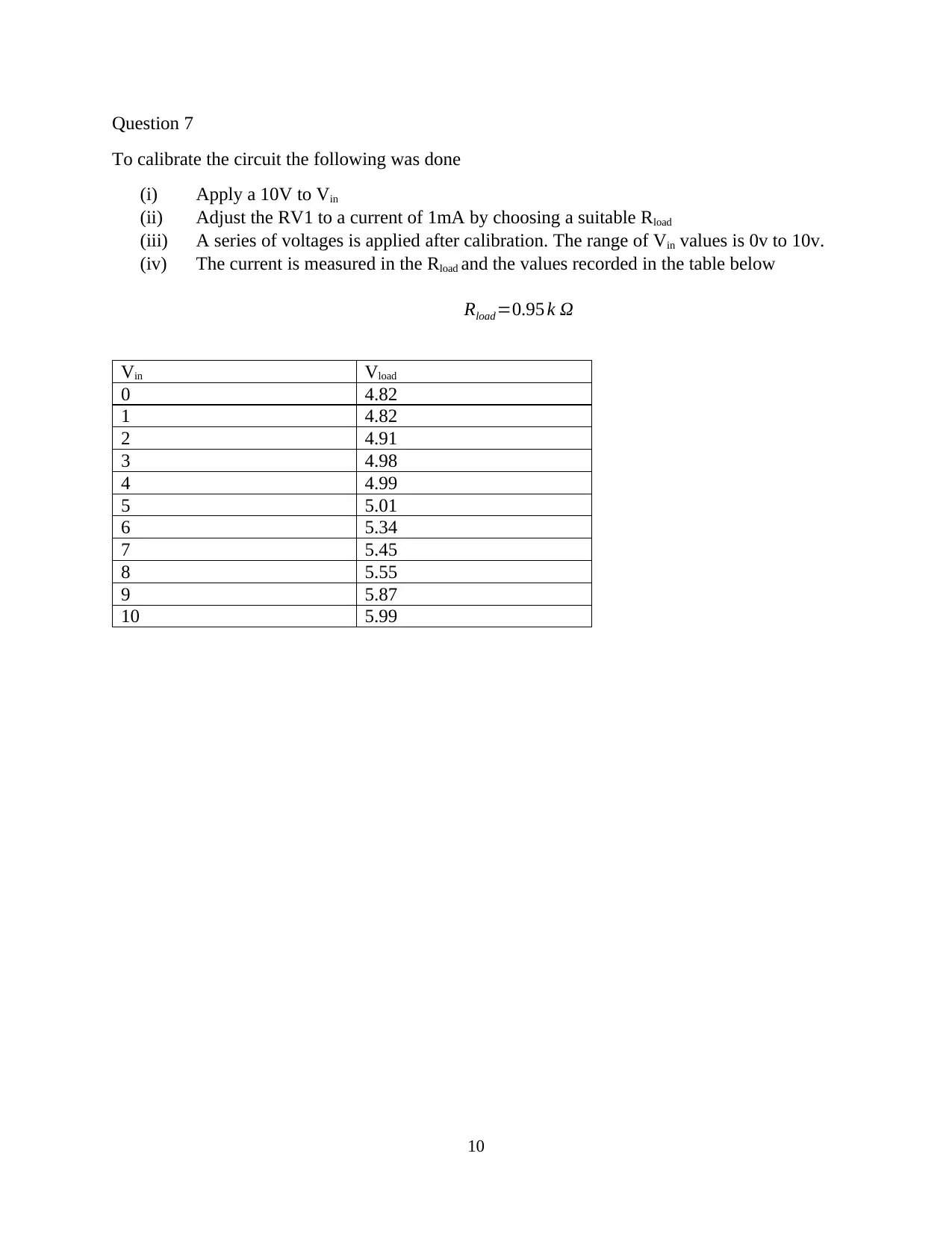
Question 7
To calibrate the circuit the following was done
(i) Apply a 10V to Vin
(ii) Adjust the RV1 to a current of 1mA by choosing a suitable Rload
(iii) A series of voltages is applied after calibration. The range of Vin values is 0v to 10v.
(iv) The current is measured in the Rload and the values recorded in the table below
Rload=0.95 k Ω
Vin Vload
0 4.82
1 4.82
2 4.91
3 4.98
4 4.99
5 5.01
6 5.34
7 5.45
8 5.55
9 5.87
10 5.99
10
Secure Best Marks with AI Grader
Need help grading? Try our AI Grader for instant feedback on your assignments.

Question 8
Adding a capacitor, clips the sinusoidal waveforms to produce a dc output. The introduced
capacitor is that of 47uF. The equivalent circuit,
11
0 2 4 6 8 10 12
0
1
2
3
4
5
6
7
f(x) = 0.120545454545455 x + 4.64545454545455
R² = 0.911533915351595
Plot of Vload against Vin
Vload
Linear (Vload)
Vin
Vload
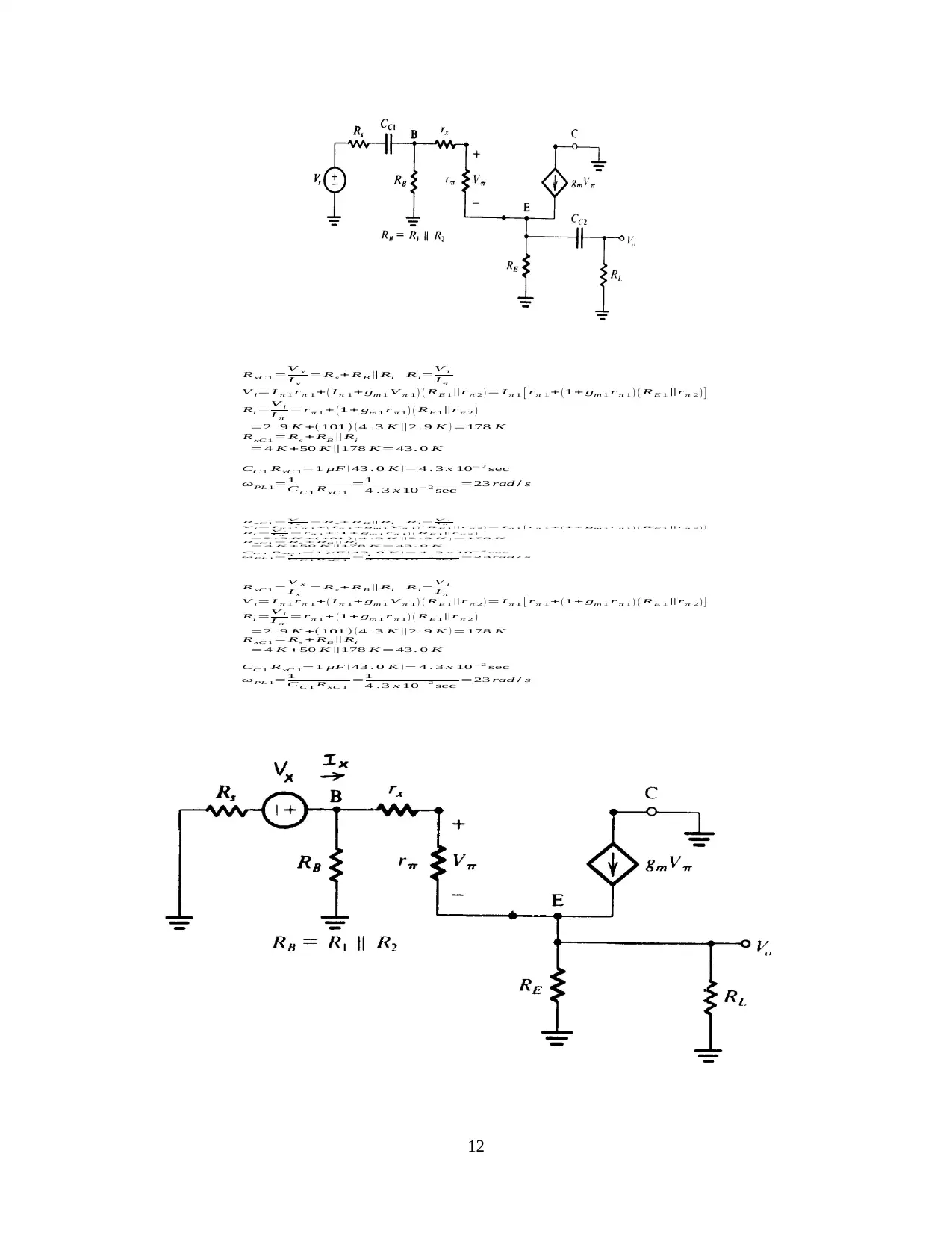
RxC 1=V x
I x
=Rs+ RB‖Ri Ri=V i
I π
V i=I π 1 rπ 1+ ( I π 1+gm 1 V π 1 ) ( RE 1‖r π 2 ) =I π 1 [ rπ 1+ ( 1+ gm 1 r π 1 ) ( RE 1‖rπ 2 ) ]
Ri =V i
I π
=rπ 1+ ( 1+ gm 1 r π 1 ) ( RE 1‖r π 2 )
=2 . 9 K +(101) ( 4 .3 K‖2 .9 K ) =178 K
RxC 1=Rs +RB‖Ri
=4 K +50 K‖178 K=43. 0 K
CC 1 RxC 1=1 μF ( 43 . 0 K ) =4 . 3 x 10⁻² sec
ωPL 1=1
CC 1 RxC 1
=1
4 .3 x 10−2 sec =23 rad / s
RxC1=V x
I x
=Rs+ RB‖Ri Ri=V i
I π
V i=I π 1 rπ 1+ ( I π 1+ gm 1 V π 1 ) ( RE 1‖r π 2 ) =I π 1 [ rπ 1+ ( 1+ gm 1 r π 1 ) ( RE 1‖rπ 2 ) ]
Ri=V i
I π
=rπ 1+ ( 1+ gm 1 r π 1 ) ( RE 1‖r π 2 )
=2 . 9 K +(101 ) ( 4 .3 K‖2 .9 K ) =178 K
RxC1=Rs + RB‖Ri
=4 K +50 K‖178 K=43. 0 K
CC 1 RxC 1=1 μF ( 43. 0 K ) =4 . 3 x 10⁻² sec
ωPL1=1
CC 1 RxC 1
=1
4 .3 x 10−2 sec =23rad / s
RxC 1=V x
I x
=Rs+ RB‖Ri Ri=V i
I π
V i=I π 1 rπ 1+ ( I π 1+ gm 1 V π 1 ) ( RE 1‖r π 2 ) =I π 1 [ rπ 1+ ( 1+ gm 1 r π 1 ) ( RE 1‖rπ 2 ) ]
Ri =V i
I π
=rπ 1+ ( 1+ gm 1 r π 1 ) ( RE 1‖r π 2 )
=2 . 9 K +(101 ) ( 4 .3 K‖2 .9 K ) =178 K
RxC 1=Rs + RB‖Ri
=4 K +50 K‖178 K=43. 0 K
CC 1 RxC 1=1 μF ( 43 . 0 K ) =4 . 3 x 10⁻² sec
ωPL 1=1
CC 1 RxC 1
=1
4 .3 x 10−2 sec =23 rad / s
12
I x
=Rs+ RB‖Ri Ri=V i
I π
V i=I π 1 rπ 1+ ( I π 1+gm 1 V π 1 ) ( RE 1‖r π 2 ) =I π 1 [ rπ 1+ ( 1+ gm 1 r π 1 ) ( RE 1‖rπ 2 ) ]
Ri =V i
I π
=rπ 1+ ( 1+ gm 1 r π 1 ) ( RE 1‖r π 2 )
=2 . 9 K +(101) ( 4 .3 K‖2 .9 K ) =178 K
RxC 1=Rs +RB‖Ri
=4 K +50 K‖178 K=43. 0 K
CC 1 RxC 1=1 μF ( 43 . 0 K ) =4 . 3 x 10⁻² sec
ωPL 1=1
CC 1 RxC 1
=1
4 .3 x 10−2 sec =23 rad / s
RxC1=V x
I x
=Rs+ RB‖Ri Ri=V i
I π
V i=I π 1 rπ 1+ ( I π 1+ gm 1 V π 1 ) ( RE 1‖r π 2 ) =I π 1 [ rπ 1+ ( 1+ gm 1 r π 1 ) ( RE 1‖rπ 2 ) ]
Ri=V i
I π
=rπ 1+ ( 1+ gm 1 r π 1 ) ( RE 1‖r π 2 )
=2 . 9 K +(101 ) ( 4 .3 K‖2 .9 K ) =178 K
RxC1=Rs + RB‖Ri
=4 K +50 K‖178 K=43. 0 K
CC 1 RxC 1=1 μF ( 43. 0 K ) =4 . 3 x 10⁻² sec
ωPL1=1
CC 1 RxC 1
=1
4 .3 x 10−2 sec =23rad / s
RxC 1=V x
I x
=Rs+ RB‖Ri Ri=V i
I π
V i=I π 1 rπ 1+ ( I π 1+ gm 1 V π 1 ) ( RE 1‖r π 2 ) =I π 1 [ rπ 1+ ( 1+ gm 1 r π 1 ) ( RE 1‖rπ 2 ) ]
Ri =V i
I π
=rπ 1+ ( 1+ gm 1 r π 1 ) ( RE 1‖r π 2 )
=2 . 9 K +(101 ) ( 4 .3 K‖2 .9 K ) =178 K
RxC 1=Rs + RB‖Ri
=4 K +50 K‖178 K=43. 0 K
CC 1 RxC 1=1 μF ( 43 . 0 K ) =4 . 3 x 10⁻² sec
ωPL 1=1
CC 1 RxC 1
=1
4 .3 x 10−2 sec =23 rad / s
12

The coupling capacitor is set at the load as a parallel. It snips out any negative current waves
generated to ensure a smooth power consumption or energy consumption by the load.
APPENDIX
(i) Data sheet for the PNP transistor attached
(ii) Data sheet for the Op-amp in Proteus Circuit design attached
13
generated to ensure a smooth power consumption or energy consumption by the load.
APPENDIX
(i) Data sheet for the PNP transistor attached
(ii) Data sheet for the Op-amp in Proteus Circuit design attached
13
1 out of 13
Your All-in-One AI-Powered Toolkit for Academic Success.
+13062052269
info@desklib.com
Available 24*7 on WhatsApp / Email
![[object Object]](/_next/static/media/star-bottom.7253800d.svg)
Unlock your academic potential
© 2024 | Zucol Services PVT LTD | All rights reserved.