Analogue Electronics Circuits: Diode, BJT, and Rectifier Report
VerifiedAdded on 2023/02/01
|20
|3349
|44
Report
AI Summary
This report delves into the realm of analogue electronics, focusing on the behavior and application of diodes and bipolar junction transistors (BJTs). The introduction highlights the importance of semiconductor materials and doping in electronic component design. The report then provides a detailed analysis of diodes, explaining the formation of the depletion layer, diode equations, and the concepts of forward and reverse bias. It also explores various diode applications, particularly in voltage rectification, including half-wave and full-wave rectifier circuits. The report then transitions to BJTs, differentiating between NPN and PNP transistors and detailing current relationships. The simulation section, conducted using Multisim software, presents the results of experiments on PN junction characteristics, including forward and reverse bias scenarios. The report concludes with observations from the simulation of a half-wave diode rectifier, both with and without a smoothing capacitor, illustrating the impact of the capacitor on output waveform smoothness. This report offers a comprehensive understanding of analogue electronics circuits and their functionalities.

Analogue Electronics Circuits 1
Student
Instructor
Analogue and digital electronics
Date
Student
Instructor
Analogue and digital electronics
Date
Paraphrase This Document
Need a fresh take? Get an instant paraphrase of this document with our AI Paraphraser
Analogue Electronics Circuits 2
Introduction
Semiconductor materials are useful when designing solid electronic components which utilize
fundamental properties of materials. Most commonly used semiconductor materials are silicon and
germanium. Behavioral characteristics of semiconductor devices are easily manipulated to conform
into required properties for applications. Such manipulation is achieved through doping
semiconductors with impurities. Electrically conductivity in semiconductors is based on the mobile
electrons and holes commonly referred to as charge carriers. Over the decades, advancement is
technology has resulted to production growth of semiconductors so as to meet the demand in their
applications. This report entails in-depth understanding of diodes and bipolar junction transistors BJT,
and selected applications. The simulation was done in Multisim software and analyzed.
Diodes
Diodes are devices belonging in the family of semiconductor that is made of two differently doped
materials namely; P-type and N-type. The P-type region encompasses holes as the majority charge
carriers and electrons as the minority charge carriers. Contrary, the N-type region accommodates
electrons as the majority charge carriers and holes as the minority charge carriers. Holes, formed by
location voids of diffused electrons, are electrically negative. The junction interface formed between
two diode regions is known as depletion layer. The depletion layer is formed when p-region and N-
region are structurally joined. In the process of formation, holes in P-region diffuse into the N-region
equally do electrons from N-region diffuse into the P-region due to mutual attraction of charges with
opposite polarity. In addition to mutual attraction, diffusion is also realized because majority charge
carrier concentration. As the diffusion proceeds, potential different is developed across the depletion
layer impeding further diffusion. An equilibrium level is achieved with the voltage across the
depletion layer, also known as potential barrier, blocking majority charge carriers from diffusing
across to the next region. In the depletion layer, there are no mobile charge carriers.
Diode equations below explain the amount of current flowing through the diode given the voltage
across and the junction’s temperature with associated physical constants.
I D =Is ( eq V D /NKT
−1 )
Where,
I D −is Diode Current
I S−is the saturation current
e−is the Eulers constant
q−is the charge of an electron
V D−Voltage across thediode
N−Emission coefficient
k −Boltzman n' s constant
T −Junctiontemperature ∈Kelvin
Analogue Electronics Circuits 3
From the equation above, kT
q is the voltage contribution within P-N junction caused by the influence
of temperature, hence thermal voltage (V ¿¿ T )¿. Thermal voltage is about 26mV at room
temperature (ARTICLES et al., 2019).
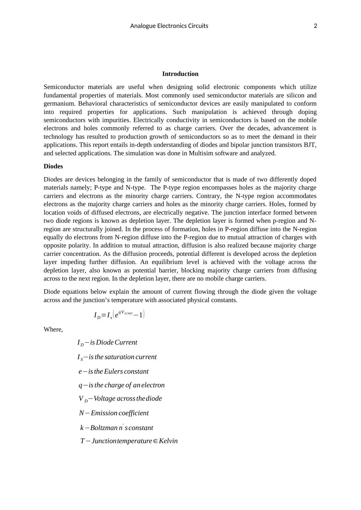
Characteristic of a diode.
The basic diode is a semiconductor which permits unidirectional flow of current when subjected
under biasing voltage. There are two types of biasing the diode namely; forward bias and reverse bias.
In forward biasing, the voltage source is connected with the diode by connecting anode to the P-
region and cathode to the N-region. However, little current will flow at lower voltage and increases
exponentially as the biasing voltage races over the potential barrier across the depletion layer.
Potential barrier varies with semiconductor materials used to make the diode. For instance, voltage of
about 0.6 to 0.7V is the permissible voltage supplied by the voltage source to breach the barrier, while
for the germanium, the value is about 0.2V. Charge carriers in forward bias consists of majority holes
and electrons. Accordingly, the diode behaves like a conductor when biasing voltage exceeds the
potential barrier. At this point, current increases linearly with increase in biasing voltage.
Similarly, diodes characteristically block flow of current under influence of the reverse biasing
voltage. In this configuration cathode of the voltage source is connected with P-region terminal of the
diode while anode is connected with the N-region of the diode. This type of configuration impacts
depletion layer by widening it. Expansion of the depletion layer is explained by drifting of majority
charge carriers away from the junction as they get attracted with the opposite polarity charged from
the reverse biasing voltage. However, for a practical diode, small reverse current leaks across the
depletion layer. This reverse current is formed by the contribution of minority charge carriers.
Minority charge carriers are electrons located in the P-region and holes located in the N-region. As the
reverse biasing voltage increases, the influence of electric field across the depletion layer becomes
greater until a point where the diode becomes conductive. The peak reverse voltage at which diode
enters conduction mode when reverse biased is known as breakdown voltage.
Graphically, the characteristics of a diode can be represented as below.
From the equation above, kT
q is the voltage contribution within P-N junction caused by the influence
of temperature, hence thermal voltage (V ¿¿ T )¿. Thermal voltage is about 26mV at room
temperature (ARTICLES et al., 2019).
Characteristic of a diode.
The basic diode is a semiconductor which permits unidirectional flow of current when subjected
under biasing voltage. There are two types of biasing the diode namely; forward bias and reverse bias.
In forward biasing, the voltage source is connected with the diode by connecting anode to the P-
region and cathode to the N-region. However, little current will flow at lower voltage and increases
exponentially as the biasing voltage races over the potential barrier across the depletion layer.
Potential barrier varies with semiconductor materials used to make the diode. For instance, voltage of
about 0.6 to 0.7V is the permissible voltage supplied by the voltage source to breach the barrier, while
for the germanium, the value is about 0.2V. Charge carriers in forward bias consists of majority holes
and electrons. Accordingly, the diode behaves like a conductor when biasing voltage exceeds the
potential barrier. At this point, current increases linearly with increase in biasing voltage.
Similarly, diodes characteristically block flow of current under influence of the reverse biasing
voltage. In this configuration cathode of the voltage source is connected with P-region terminal of the
diode while anode is connected with the N-region of the diode. This type of configuration impacts
depletion layer by widening it. Expansion of the depletion layer is explained by drifting of majority
charge carriers away from the junction as they get attracted with the opposite polarity charged from
the reverse biasing voltage. However, for a practical diode, small reverse current leaks across the
depletion layer. This reverse current is formed by the contribution of minority charge carriers.
Minority charge carriers are electrons located in the P-region and holes located in the N-region. As the
reverse biasing voltage increases, the influence of electric field across the depletion layer becomes
greater until a point where the diode becomes conductive. The peak reverse voltage at which diode
enters conduction mode when reverse biased is known as breakdown voltage.
Graphically, the characteristics of a diode can be represented as below.
You're viewing a preview
Unlock full access by subscribing today!
Analogue Electronics Circuits 4
Applications of diodes
Inherent characteristics of diodes enable these type of semiconductor to be used over an extensive
range of applications. Applicability of diodes narrows down to individual characteristics of the
specific diode. For instance, in power rectification, special class of diodes known as rectifier diodes
are used while for voltage regulation, zener diodes are preferred.
Voltage rectification
Rectifier is a circuit that allows alternating current and or voltage to flow with the same polarity and
in the same direction (ElProCus - Electronic Projects for Engineering Students, 2019).
Power diodes are connected together or singly configured to produce two types of rectifier circuits
namely; Half wave and bridge rectifier.
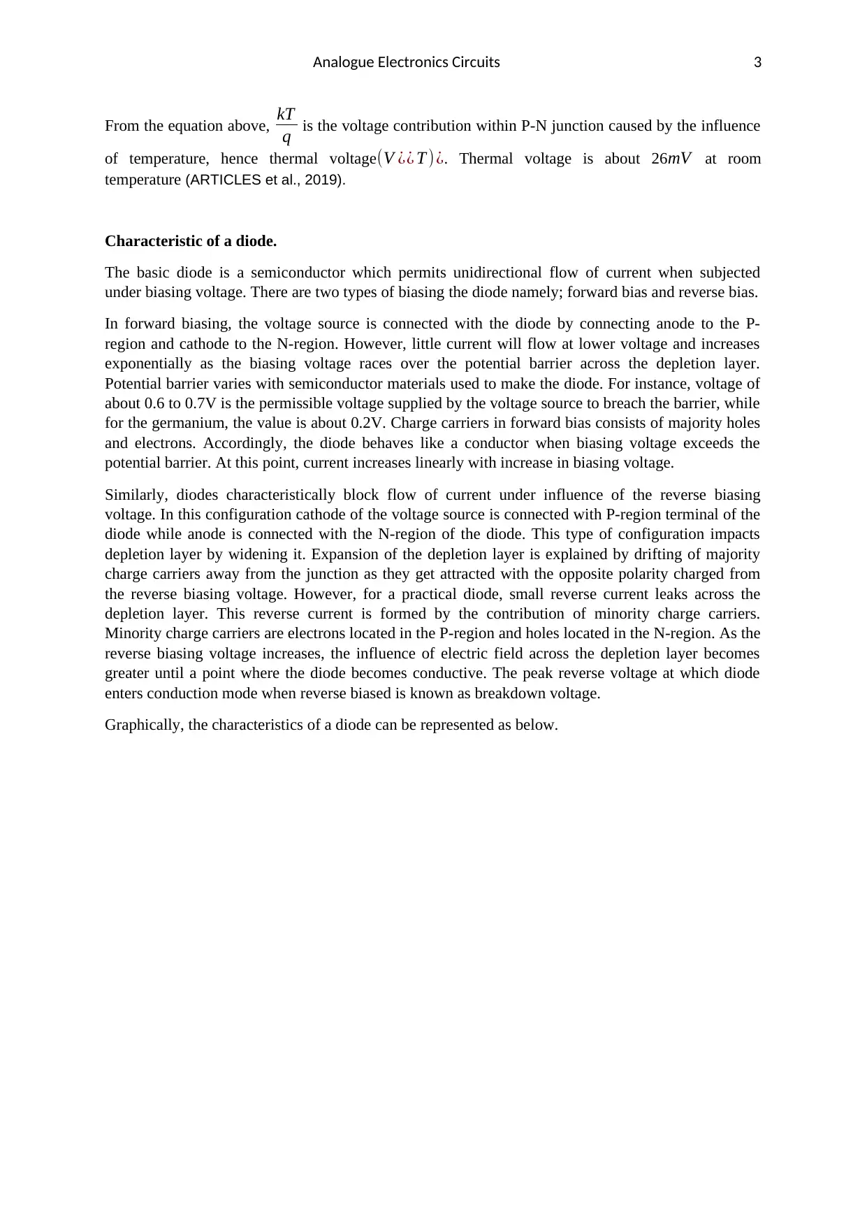
A half wave diode rectifier consist of a single diode connected in series with the load and the AC
power source. Rectification is achieved by allowing either positive or negative half cycle of the
alternating signals to pass through it and chopping off the other opposite half cycle. Accordingly, the
diode is forward biased during the conducting half cycle and become reverse biased during non-
conducting half cycle. By doing so, the load current becomes unidirectional. The output voltage
profile is irregular because of spikes that are in phase with the conducting half cycle as below
Applications of diodes
Inherent characteristics of diodes enable these type of semiconductor to be used over an extensive
range of applications. Applicability of diodes narrows down to individual characteristics of the
specific diode. For instance, in power rectification, special class of diodes known as rectifier diodes
are used while for voltage regulation, zener diodes are preferred.
Voltage rectification
Rectifier is a circuit that allows alternating current and or voltage to flow with the same polarity and
in the same direction (ElProCus - Electronic Projects for Engineering Students, 2019).
Power diodes are connected together or singly configured to produce two types of rectifier circuits
namely; Half wave and bridge rectifier.
A half wave diode rectifier consist of a single diode connected in series with the load and the AC
power source. Rectification is achieved by allowing either positive or negative half cycle of the
alternating signals to pass through it and chopping off the other opposite half cycle. Accordingly, the
diode is forward biased during the conducting half cycle and become reverse biased during non-
conducting half cycle. By doing so, the load current becomes unidirectional. The output voltage
profile is irregular because of spikes that are in phase with the conducting half cycle as below
Paraphrase This Document
Need a fresh take? Get an instant paraphrase of this document with our AI Paraphraser
Analogue Electronics Circuits 5
The average output voltage is determined using the equation below.
V D= V max
π =0.318V max
Or
V D=0.45 V rms
The rectifier is about 50% efficient since only a half of the power is supplied to the load. Undesirable
ripples at the output can be significantly reduced by connecting a capacitor in parallel with the load or
across the output terminals. The size of the capacitor depends with the load resistance whose
resistance directly affects RC time constant of the capacitor.
Full wave diode rectifier is achieved by use of two or more diodes in the rectification circuit. One
such type forms bridge rectifier which consists of four diodes connected in a closed loop. In
operation, two paired diodes conduct every positive half cycle respectively. The voltage formed
across the load is in phase with unidirectional current.
The average output DC voltage is determined by the equation below;
V D= 2 V max
π =0.637 V max=0.9 V rms
Ripples at the output signal is twice the frequency of ripples in half wave rectifier’s output.
Bipolar Junction Transistor.
A bipolar junction transistor is a solid device in the family of semiconductor formed by three doped
regions. There are two type of BJTs namely, NPN and PNP. The distinction is brought in by types of
regions sandwiching the base region. As the name suggests, NPN is formed by sandwiching a thin
layer of positively doped base material between richly negative-doped collector and emitter. On the
other side, PNP is synthesized by sandwiching thin layer of positively doped base between negatively
doped emitter and collector. There exist potential barrier of about 0.6V between the junction made by
base and emitter. Considering the diagram below, current relationship in the transmitter can be
determined as in the equations below.
I E =IC + IB
Where I E −is emitter current
IC∧IB−are collector∧base current respectively
Analogue Electronics Circuits 6
Current gain of the BJT is;
β= IC
IB
The current gain between collector and emitter is given by;
α= IC
IE
The relationship between β∧α is determined by;
β= α
1−α and α= β
1+ β
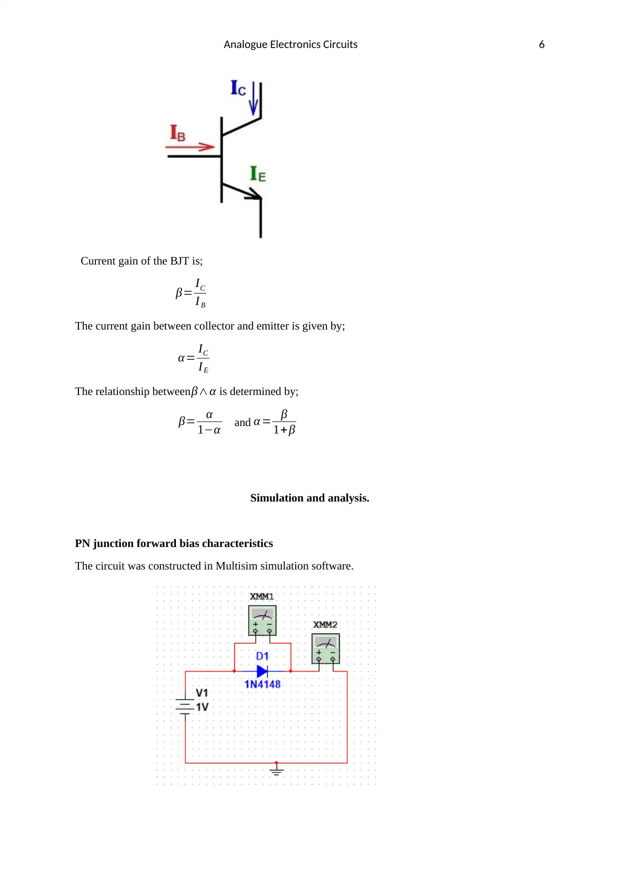
Simulation and analysis.
PN junction forward bias characteristics
The circuit was constructed in Multisim simulation software.
Current gain of the BJT is;
β= IC
IB
The current gain between collector and emitter is given by;
α= IC
IE
The relationship between β∧α is determined by;
β= α
1−α and α= β
1+ β
Simulation and analysis.
PN junction forward bias characteristics
The circuit was constructed in Multisim simulation software.
You're viewing a preview
Unlock full access by subscribing today!
Analogue Electronics Circuits 7
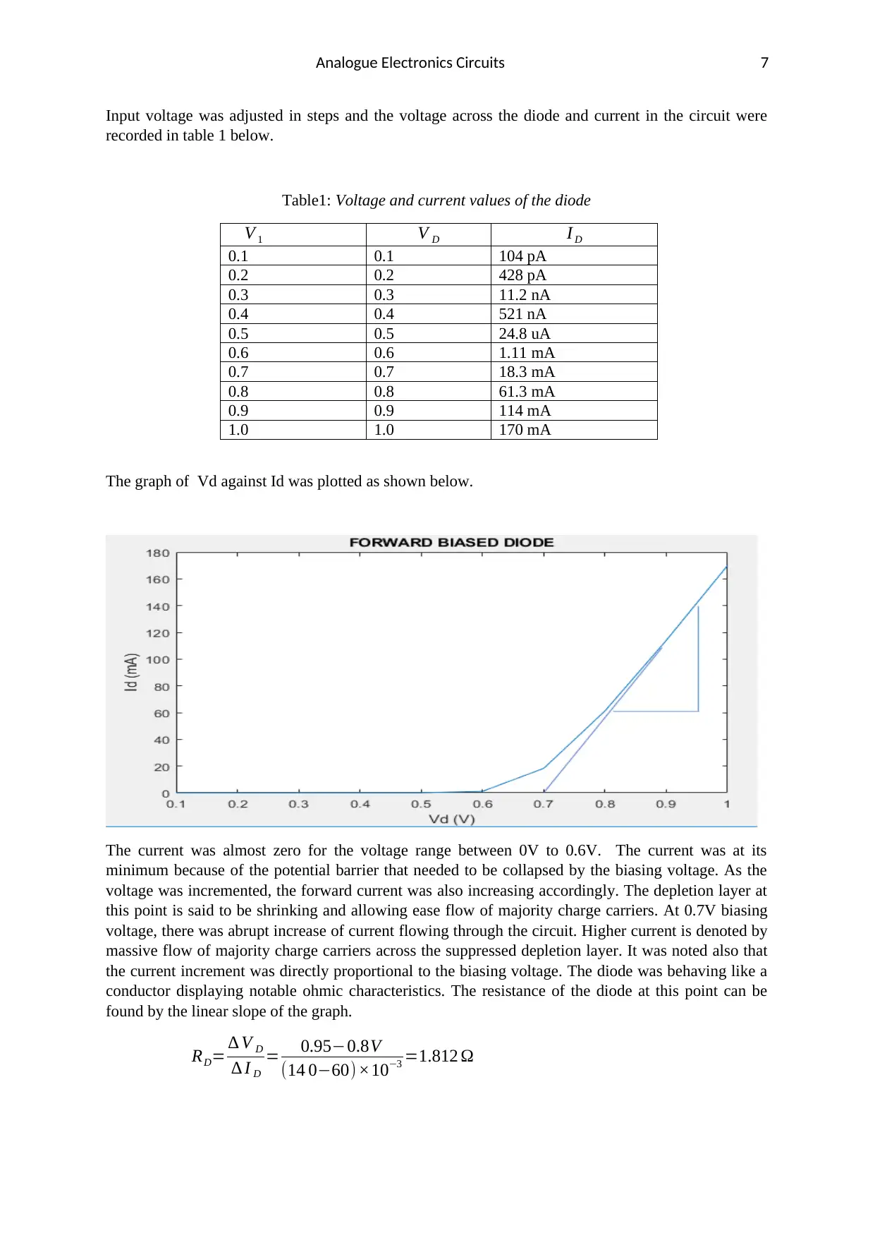
Input voltage was adjusted in steps and the voltage across the diode and current in the circuit were
recorded in table 1 below.
Table1: Voltage and current values of the diode
V 1 V D I D
0.1 0.1 104 pA
0.2 0.2 428 pA
0.3 0.3 11.2 nA
0.4 0.4 521 nA
0.5 0.5 24.8 uA
0.6 0.6 1.11 mA
0.7 0.7 18.3 mA
0.8 0.8 61.3 mA
0.9 0.9 114 mA
1.0 1.0 170 mA
The graph of Vd against Id was plotted as shown below.
The current was almost zero for the voltage range between 0V to 0.6V. The current was at its
minimum because of the potential barrier that needed to be collapsed by the biasing voltage. As the
voltage was incremented, the forward current was also increasing accordingly. The depletion layer at
this point is said to be shrinking and allowing ease flow of majority charge carriers. At 0.7V biasing
voltage, there was abrupt increase of current flowing through the circuit. Higher current is denoted by
massive flow of majority charge carriers across the suppressed depletion layer. It was noted also that
the current increment was directly proportional to the biasing voltage. The diode was behaving like a
conductor displaying notable ohmic characteristics. The resistance of the diode at this point can be
found by the linear slope of the graph.
RD= ∆ V D
∆ I D
= 0.95−0.8V
(14 0−60) ×10−3 =1.812 Ω
Paraphrase This Document
Need a fresh take? Get an instant paraphrase of this document with our AI Paraphraser
Analogue Electronics Circuits 8
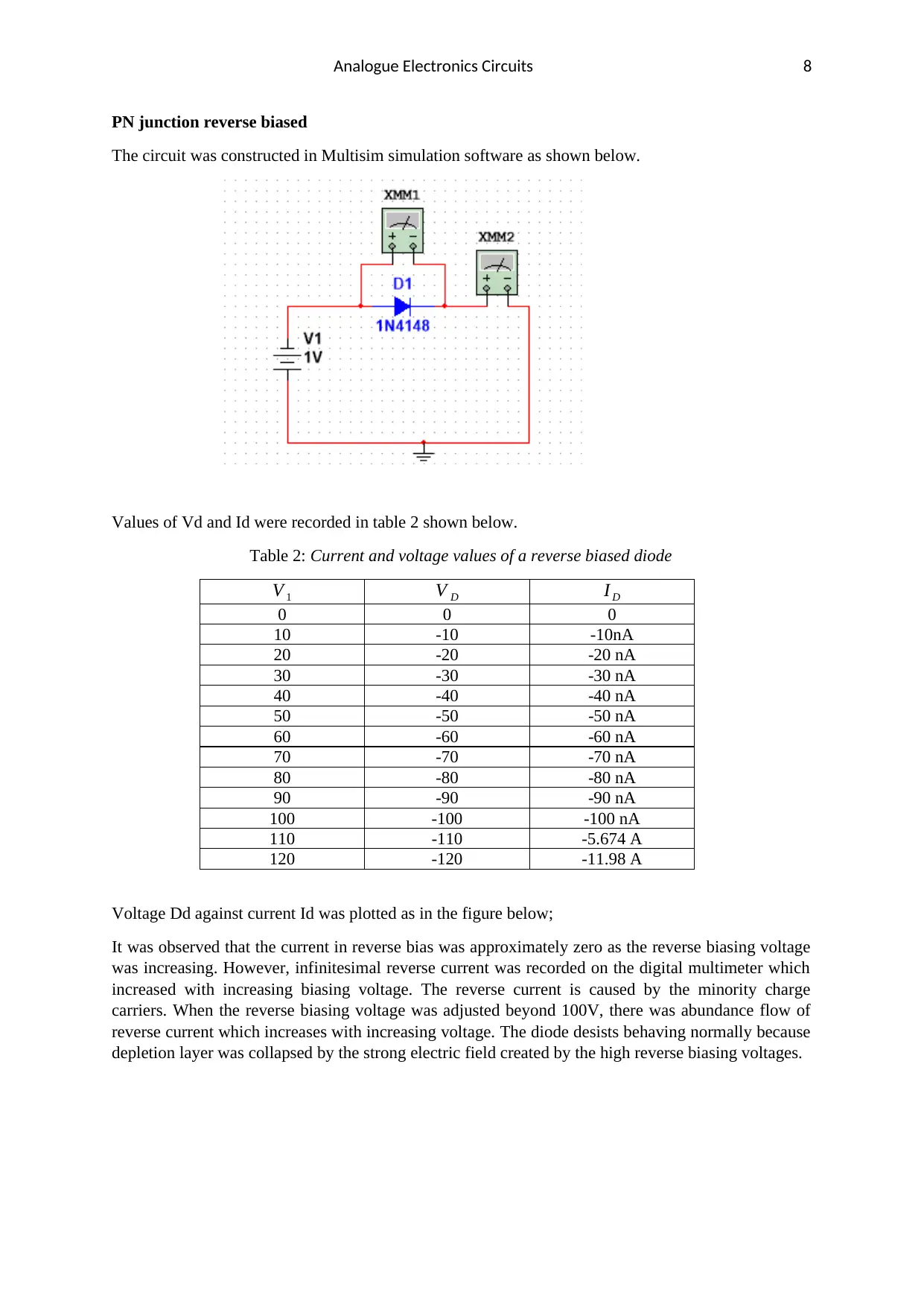
PN junction reverse biased
The circuit was constructed in Multisim simulation software as shown below.
Values of Vd and Id were recorded in table 2 shown below.
Table 2: Current and voltage values of a reverse biased diode
V 1 V D I D
0 0 0
10 -10 -10nA
20 -20 -20 nA
30 -30 -30 nA
40 -40 -40 nA
50 -50 -50 nA
60 -60 -60 nA
70 -70 -70 nA
80 -80 -80 nA
90 -90 -90 nA
100 -100 -100 nA
110 -110 -5.674 A
120 -120 -11.98 A
Voltage Dd against current Id was plotted as in the figure below;
It was observed that the current in reverse bias was approximately zero as the reverse biasing voltage
was increasing. However, infinitesimal reverse current was recorded on the digital multimeter which
increased with increasing biasing voltage. The reverse current is caused by the minority charge
carriers. When the reverse biasing voltage was adjusted beyond 100V, there was abundance flow of
reverse current which increases with increasing voltage. The diode desists behaving normally because
depletion layer was collapsed by the strong electric field created by the high reverse biasing voltages.
Analogue Electronics Circuits 9
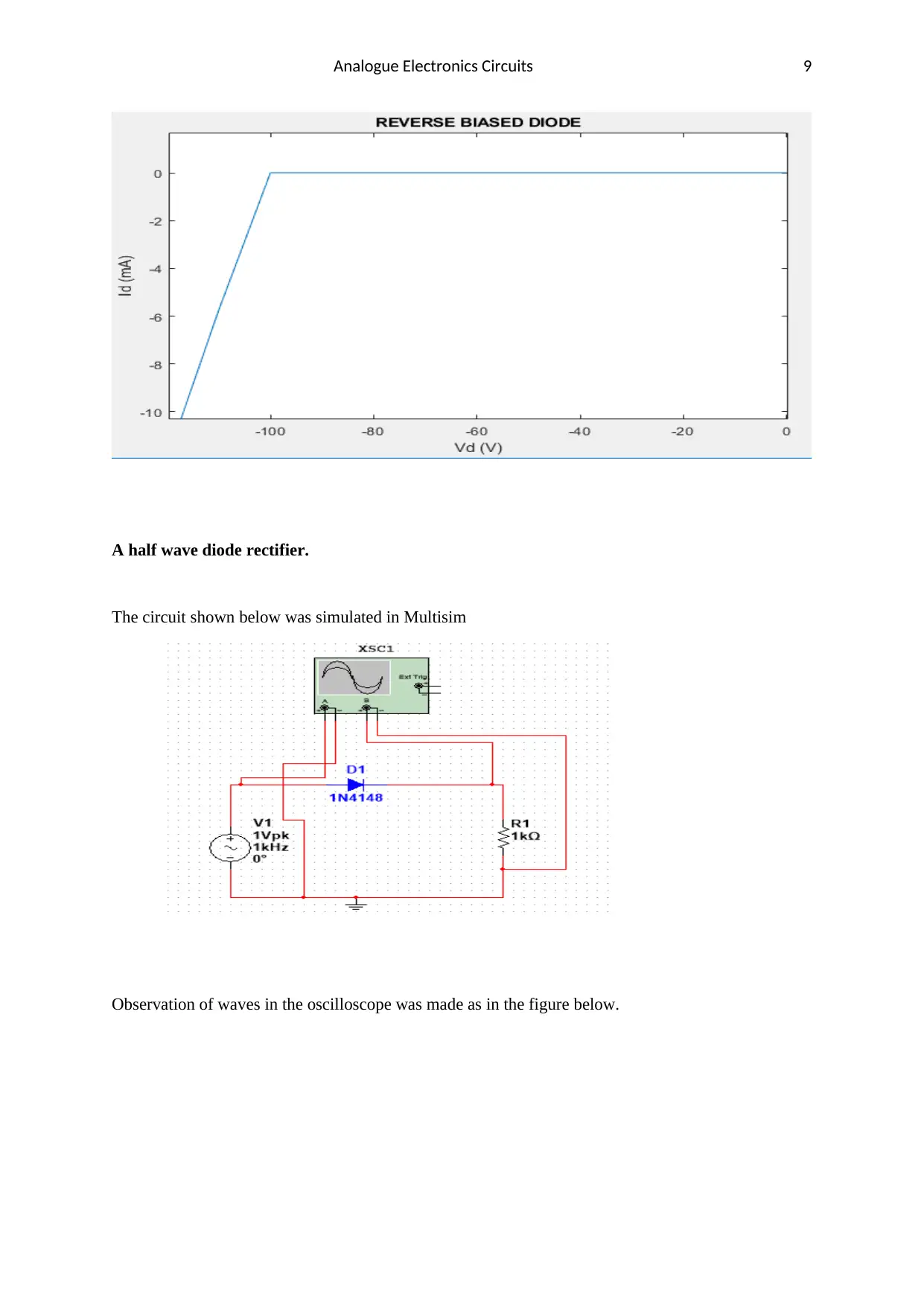
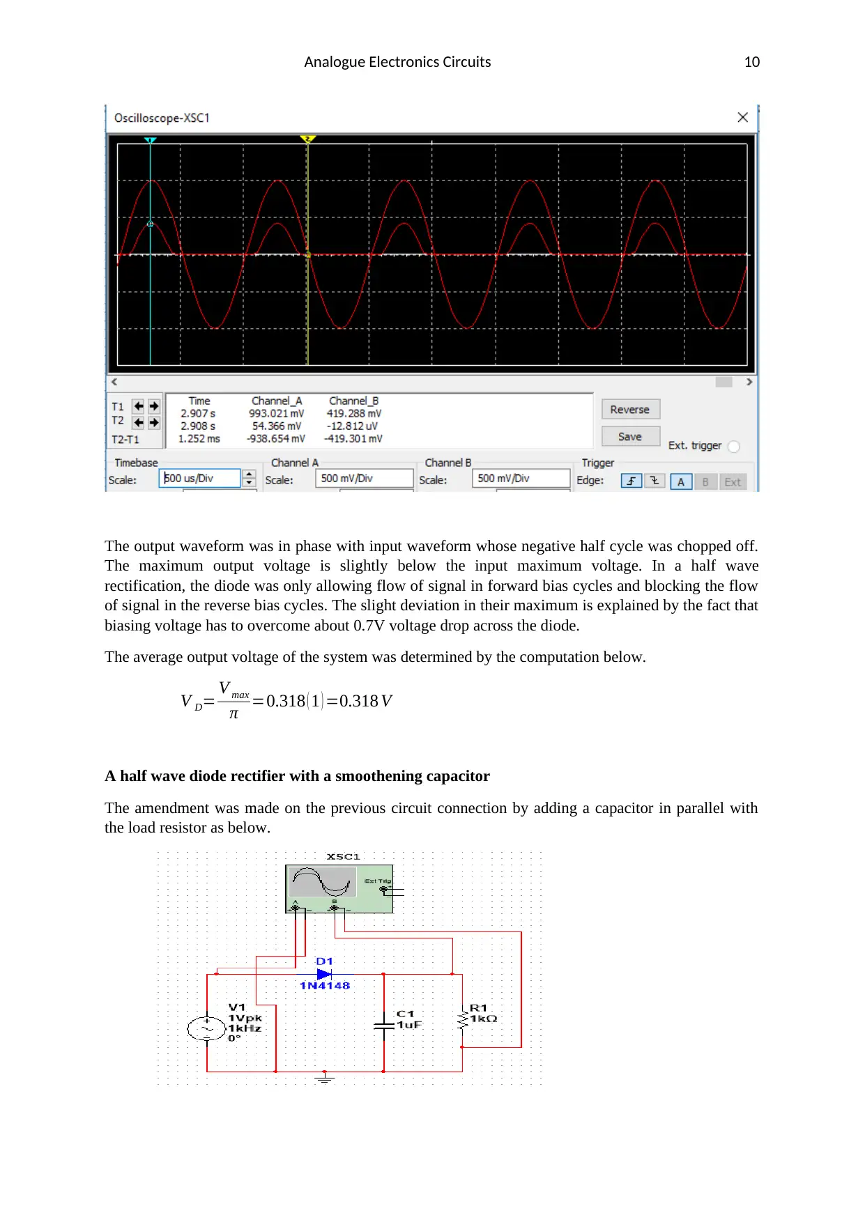
A half wave diode rectifier.
The circuit shown below was simulated in Multisim
Observation of waves in the oscilloscope was made as in the figure below.
A half wave diode rectifier.
The circuit shown below was simulated in Multisim
Observation of waves in the oscilloscope was made as in the figure below.
You're viewing a preview
Unlock full access by subscribing today!
Analogue Electronics Circuits 10
The output waveform was in phase with input waveform whose negative half cycle was chopped off.
The maximum output voltage is slightly below the input maximum voltage. In a half wave
rectification, the diode was only allowing flow of signal in forward bias cycles and blocking the flow
of signal in the reverse bias cycles. The slight deviation in their maximum is explained by the fact that
biasing voltage has to overcome about 0.7V voltage drop across the diode.
The average output voltage of the system was determined by the computation below.
V D= V max
π =0.318 ( 1 ) =0.318 V
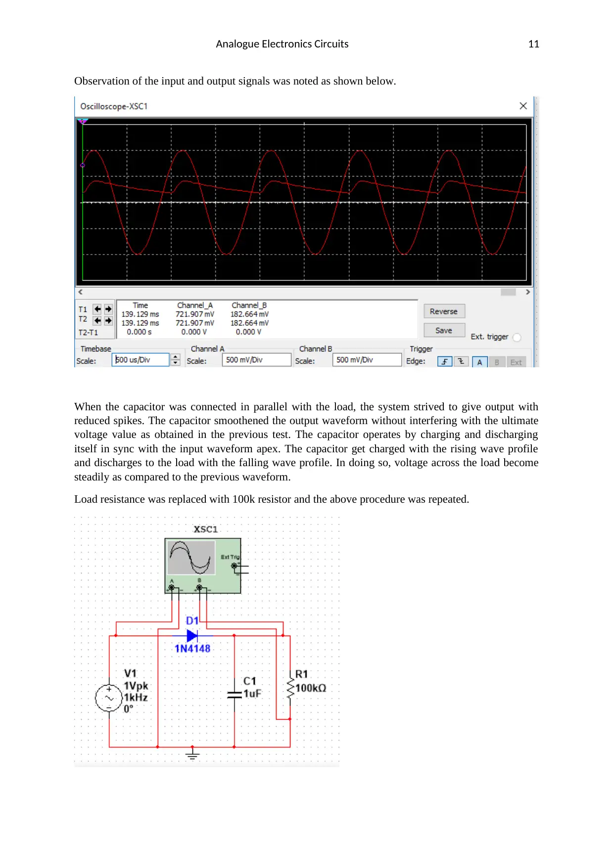
A half wave diode rectifier with a smoothening capacitor
The amendment was made on the previous circuit connection by adding a capacitor in parallel with
the load resistor as below.
The output waveform was in phase with input waveform whose negative half cycle was chopped off.
The maximum output voltage is slightly below the input maximum voltage. In a half wave
rectification, the diode was only allowing flow of signal in forward bias cycles and blocking the flow
of signal in the reverse bias cycles. The slight deviation in their maximum is explained by the fact that
biasing voltage has to overcome about 0.7V voltage drop across the diode.
The average output voltage of the system was determined by the computation below.
V D= V max
π =0.318 ( 1 ) =0.318 V
A half wave diode rectifier with a smoothening capacitor
The amendment was made on the previous circuit connection by adding a capacitor in parallel with
the load resistor as below.
Paraphrase This Document
Need a fresh take? Get an instant paraphrase of this document with our AI Paraphraser
Analogue Electronics Circuits 11
Observation of the input and output signals was noted as shown below.
When the capacitor was connected in parallel with the load, the system strived to give output with
reduced spikes. The capacitor smoothened the output waveform without interfering with the ultimate
voltage value as obtained in the previous test. The capacitor operates by charging and discharging
itself in sync with the input waveform apex. The capacitor get charged with the rising wave profile
and discharges to the load with the falling wave profile. In doing so, voltage across the load become
steadily as compared to the previous waveform.
Load resistance was replaced with 100k resistor and the above procedure was repeated.
Analogue Electronics Circuits 12
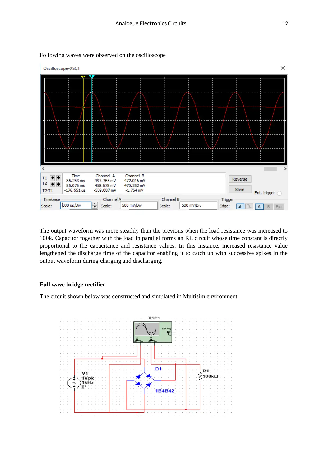
Following waves were observed on the oscilloscope
The output waveform was more steadily than the previous when the load resistance was increased to
100k. Capacitor together with the load in parallel forms an RL circuit whose time constant is directly
proportional to the capacitance and resistance values. In this instance, increased resistance value
lengthened the discharge time of the capacitor enabling it to catch up with successive spikes in the
output waveform during charging and discharging.
Full wave bridge rectifier
The circuit shown below was constructed and simulated in Multisim environment.
You're viewing a preview
Unlock full access by subscribing today!
Analogue Electronics Circuits 13
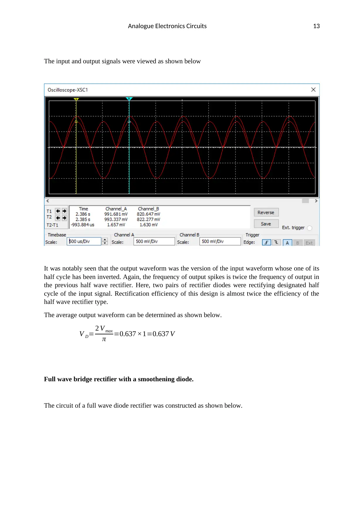
The input and output signals were viewed as shown below
It was notably seen that the output waveform was the version of the input waveform whose one of its
half cycle has been inverted. Again, the frequency of output spikes is twice the frequency of output in
the previous half wave rectifier. Here, two pairs of rectifier diodes were rectifying designated half
cycle of the input signal. Rectification efficiency of this design is almost twice the efficiency of the
half wave rectifier type.
The average output waveform can be determined as shown below.
V D= 2 V max
π =0.637 ×1=0.637 V
Full wave bridge rectifier with a smoothening diode.
The circuit of a full wave diode rectifier was constructed as shown below.
Paraphrase This Document
Need a fresh take? Get an instant paraphrase of this document with our AI Paraphraser
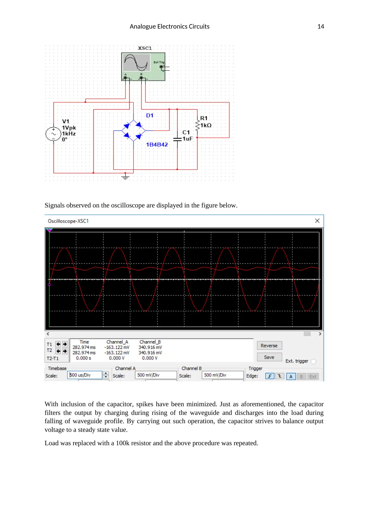
Analogue Electronics Circuits 14
Signals observed on the oscilloscope are displayed in the figure below.
With inclusion of the capacitor, spikes have been minimized. Just as aforementioned, the capacitor
filters the output by charging during rising of the waveguide and discharges into the load during
falling of waveguide profile. By carrying out such operation, the capacitor strives to balance output
voltage to a steady state value.
Load was replaced with a 100k resistor and the above procedure was repeated.
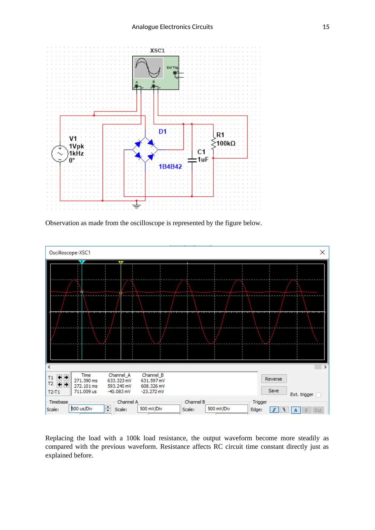
Analogue Electronics Circuits 15
Observation as made from the oscilloscope is represented by the figure below.
Replacing the load with a 100k load resistance, the output waveform become more steadily as
compared with the previous waveform. Resistance affects RC circuit time constant directly just as
explained before.
Observation as made from the oscilloscope is represented by the figure below.
Replacing the load with a 100k load resistance, the output waveform become more steadily as
compared with the previous waveform. Resistance affects RC circuit time constant directly just as
explained before.
You're viewing a preview
Unlock full access by subscribing today!
Analogue Electronics Circuits 16
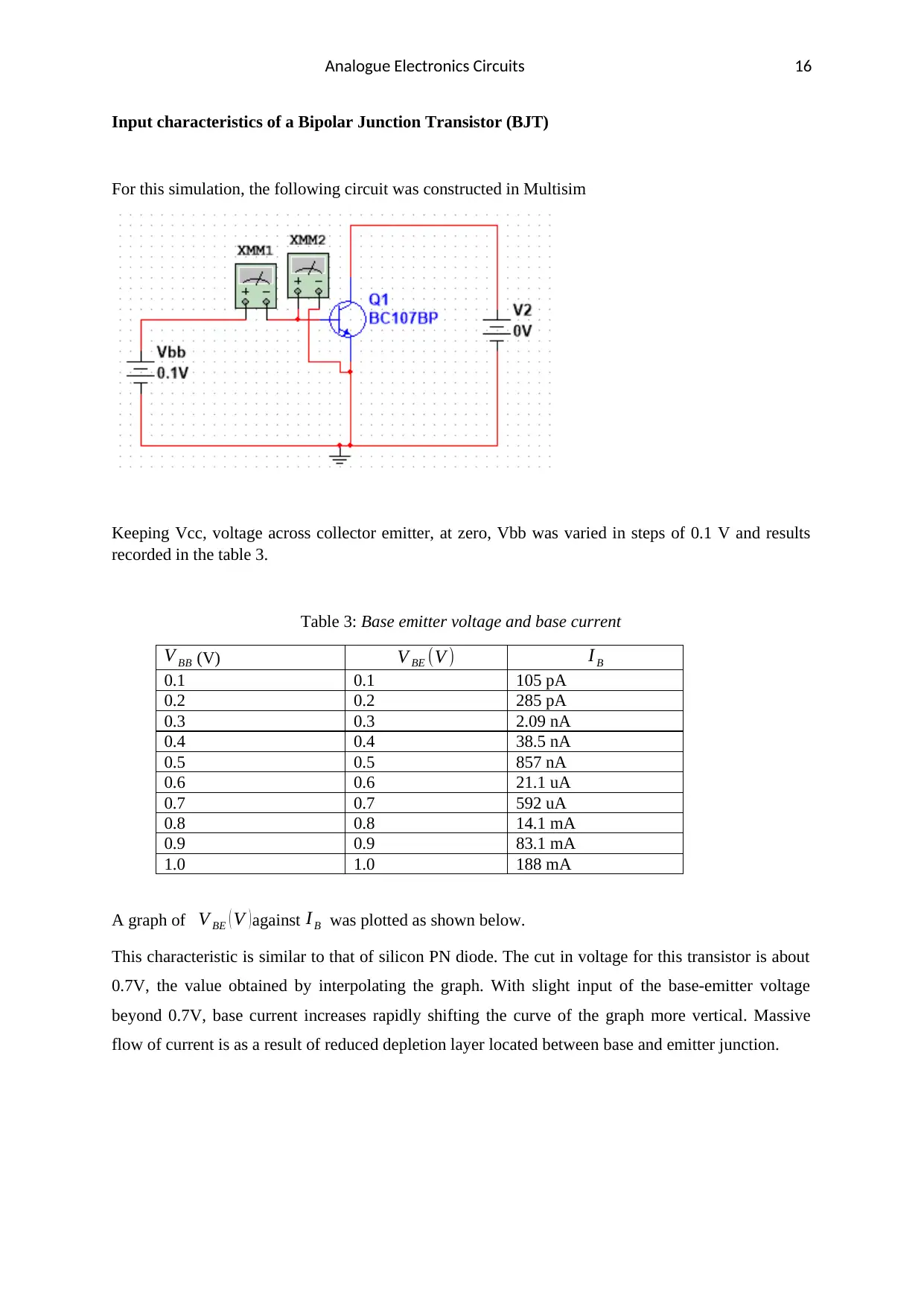
Input characteristics of a Bipolar Junction Transistor (BJT)
For this simulation, the following circuit was constructed in Multisim
Keeping Vcc, voltage across collector emitter, at zero, Vbb was varied in steps of 0.1 V and results
recorded in the table 3.
Table 3: Base emitter voltage and base current
V BB (V) V BE (V ) I B
0.1 0.1 105 pA
0.2 0.2 285 pA
0.3 0.3 2.09 nA
0.4 0.4 38.5 nA
0.5 0.5 857 nA
0.6 0.6 21.1 uA
0.7 0.7 592 uA
0.8 0.8 14.1 mA
0.9 0.9 83.1 mA
1.0 1.0 188 mA
A graph of V BE ( V )against I B was plotted as shown below.
This characteristic is similar to that of silicon PN diode. The cut in voltage for this transistor is about
0.7V, the value obtained by interpolating the graph. With slight input of the base-emitter voltage
beyond 0.7V, base current increases rapidly shifting the curve of the graph more vertical. Massive
flow of current is as a result of reduced depletion layer located between base and emitter junction.
Paraphrase This Document
Need a fresh take? Get an instant paraphrase of this document with our AI Paraphraser
Analogue Electronics Circuits 17
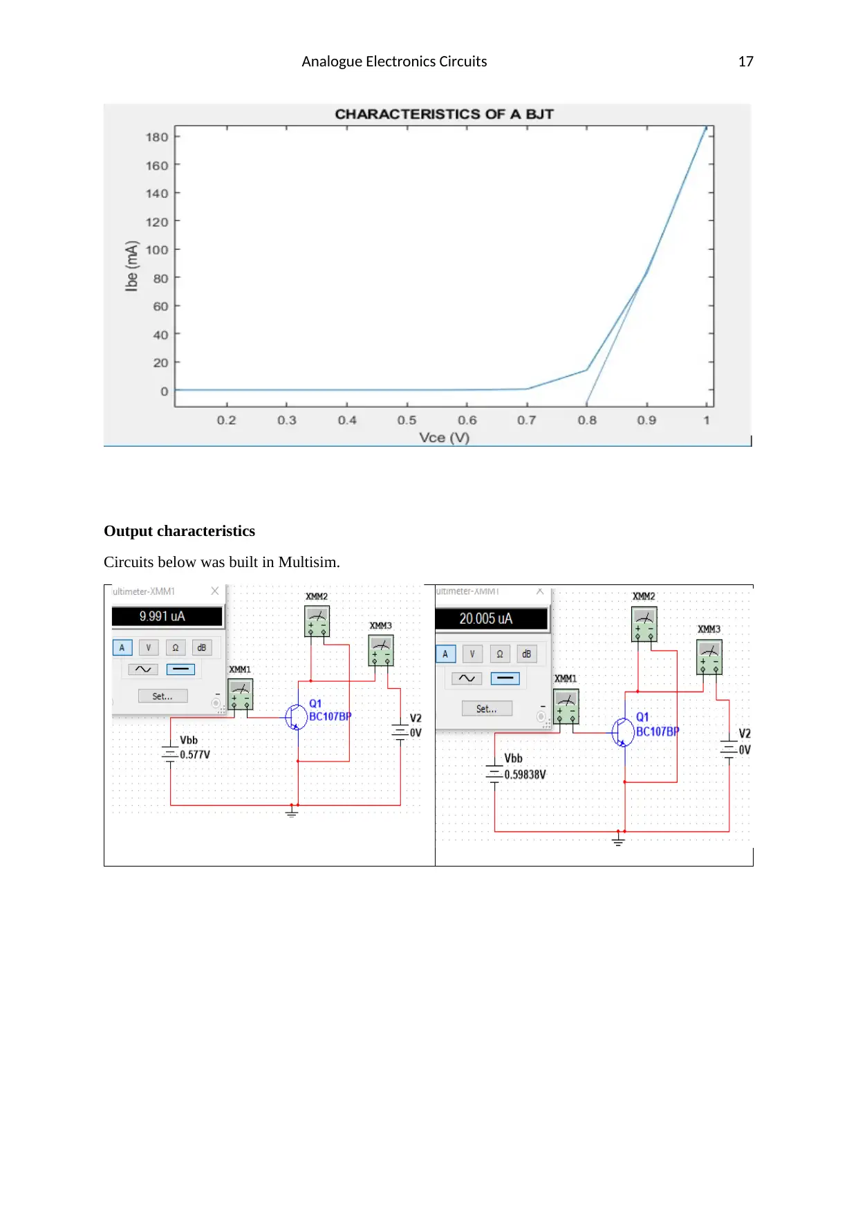
Output characteristics
Circuits below was built in Multisim.
Output characteristics
Circuits below was built in Multisim.
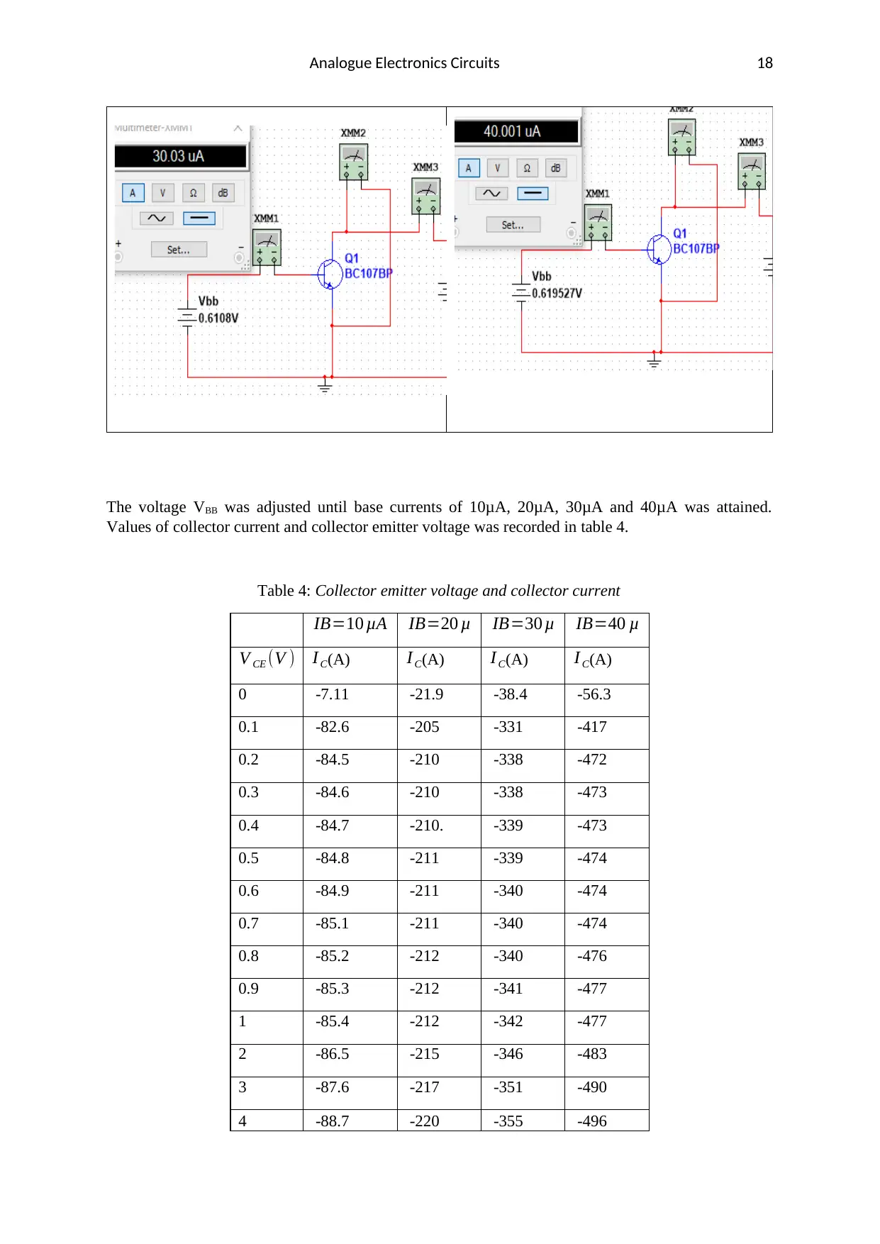
Analogue Electronics Circuits 18
The voltage VBB was adjusted until base currents of 10μA, 20μA, 30μA and 40μA was attained.
Values of collector current and collector emitter voltage was recorded in table 4.
Table 4: Collector emitter voltage and collector current
IB=10 μA IB=20 μ IB=30 μ IB=40 μ
V CE (V ) I C(A) I C(A) I C(A) I C(A)
0 -7.11 -21.9 -38.4 -56.3
0.1 -82.6 -205 -331 -417
0.2 -84.5 -210 -338 -472
0.3 -84.6 -210 -338 -473
0.4 -84.7 -210. -339 -473
0.5 -84.8 -211 -339 -474
0.6 -84.9 -211 -340 -474
0.7 -85.1 -211 -340 -474
0.8 -85.2 -212 -340 -476
0.9 -85.3 -212 -341 -477
1 -85.4 -212 -342 -477
2 -86.5 -215 -346 -483
3 -87.6 -217 -351 -490
4 -88.7 -220 -355 -496
You're viewing a preview
Unlock full access by subscribing today!
Analogue Electronics Circuits 19
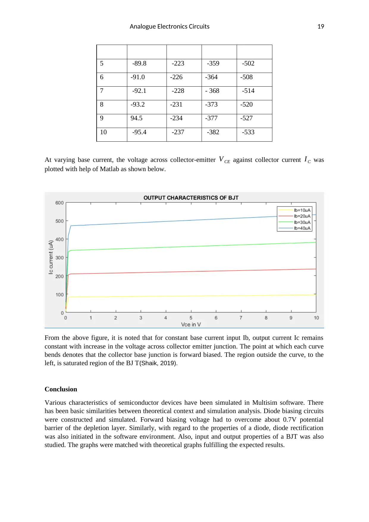
5 -89.8 -223 -359 -502
6 -91.0 -226 -364 -508
7 -92.1 -228 - 368 -514
8 -93.2 -231 -373 -520
9 94.5 -234 -377 -527
10 -95.4 -237 -382 -533
At varying base current, the voltage across collector-emitter V CE against collector current I C was
plotted with help of Matlab as shown below.
From the above figure, it is noted that for constant base current input Ib, output current Ic remains
constant with increase in the voltage across collector emitter junction. The point at which each curve
bends denotes that the collector base junction is forward biased. The region outside the curve, to the
left, is saturated region of the BJ T(Shaik, 2019).
Conclusion
Various characteristics of semiconductor devices have been simulated in Multisim software. There
has been basic similarities between theoretical context and simulation analysis. Diode biasing circuits
were constructed and simulated. Forward biasing voltage had to overcome about 0.7V potential
barrier of the depletion layer. Similarly, with regard to the properties of a diode, diode rectification
was also initiated in the software environment. Also, input and output properties of a BJT was also
studied. The graphs were matched with theoretical graphs fulfilling the expected results.
Paraphrase This Document
Need a fresh take? Get an instant paraphrase of this document with our AI Paraphraser
Analogue Electronics Circuits 20
Reference
ARTICLES, T., PRODUCTS, N., ELECTRONICS, G., PROJECTS, C., MICRO, E., Lectures, V.,
Webinars, I., Training, I., Search, P., DB, T., Tool, B. and Designs, R. (2019). Introduction to
Diodes And Rectifiers | Diodes and Rectifiers | Electronics Textbook. [Online]
Allaboutcircuits.com. Available at:
https://www.allaboutcircuits.com/textbook/semiconductors/chpt-3/introduction-to-diodes-and-
rectifiers/
ElProCus - Electronic Projects for Engineering Students. (2019). Introduction to Rectifier Diode Circuit
Working and Its Applications. [Online] Available at: https://www.elprocus.com/rectifier-diode-
working-applications/
Shaik, A. (2019). Common Base (CB) Configuration or Common Base Amplifier. [Online] Physics-
and-radio-electronics.com. Available at:
https://www.physics-and-radio-electronics.com/electronic-devices-and-circuits/transistors/
bipolarjunctiontransistor/commonbaseconfiguration.html
1 out of 20
Related Documents


Your All-in-One AI-Powered Toolkit for Academic Success.
+13062052269
info@desklib.com
Available 24*7 on WhatsApp / Email
![[object Object]](/_next/static/media/star-bottom.7253800d.svg)
Unlock your academic potential
© 2024 | Zucol Services PVT LTD | All rights reserved.