Memory Design and Instruction Set Architecture

Verified

Added on  2020/04/07

|6
|487
|87
AI Summary
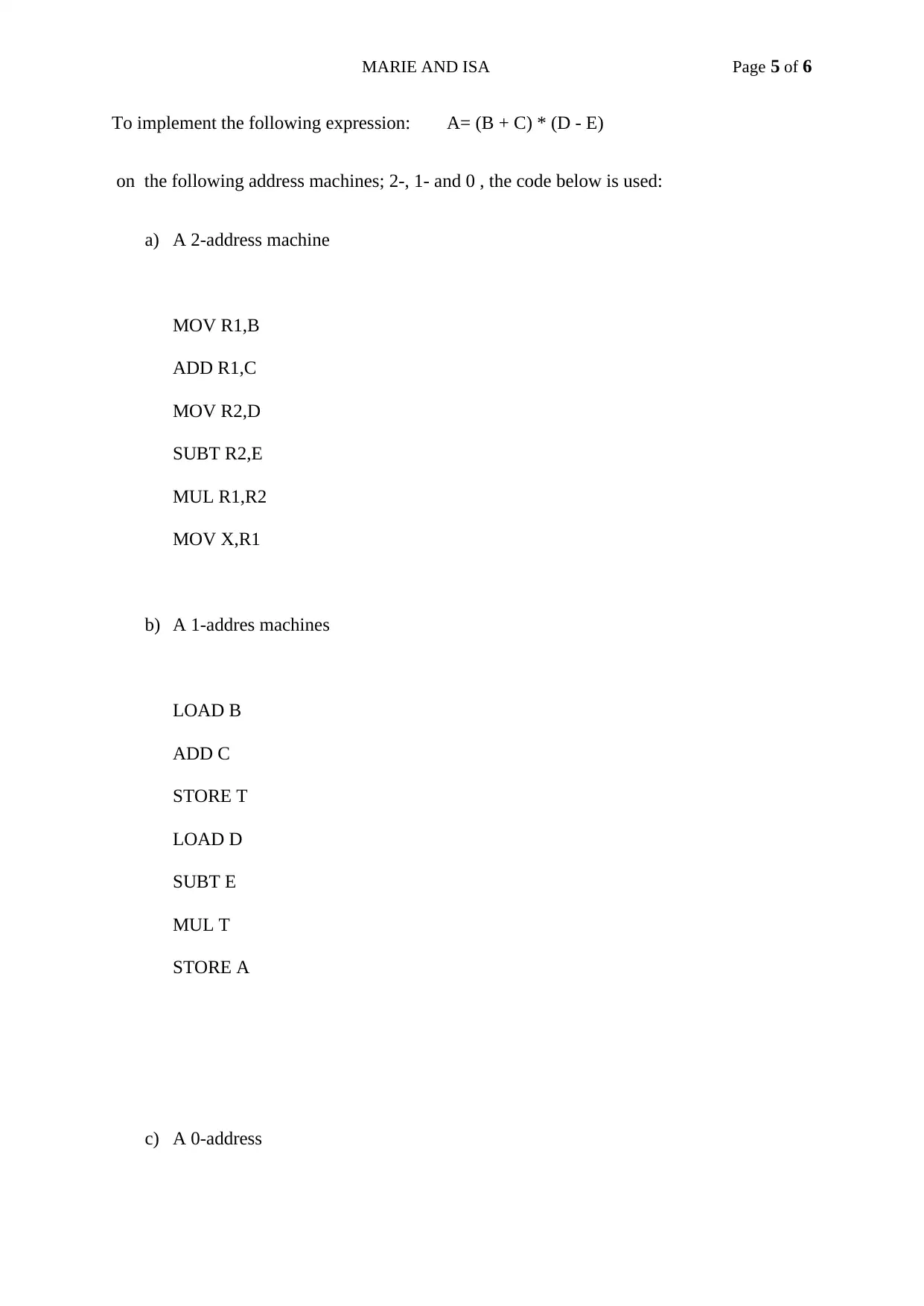
This assignment delves into the concepts of memory design and instruction set architecture. It involves calculating the number of RAM chips required for a specific memory capacity, determining address bits, and analyzing different addressing modes. The assignment also explores how to implement instructions using various addressing modes and illustrates the code for a given arithmetic expression in 2-, 1-, and 0-address machines.
tabler-icon-diamond-filled.svg

Contribute Materials

Your contribution can guide someone’s learning journey. Share your documents today.
Document Page
Page 1 of 6
Running head: MARIE AND ISA
ASSIGNMENT 2: MARIE & ISA
SUBJECT CODE: ITC544
NAME
STUDENT ID
tabler-icon-diamond-filled.svg

Secure Best Marks with AI Grader

Need help grading? Try our AI Grader for instant feedback on your assignments.
Document Page
MARIE AND ISA Page 2 of 6
Question 1
RAM chips of capacity 1024 K *32are used to build a memory of 256M * 128 capacity.
From this information, it is possible to determine the number of RAM chips necessary to
build the memory, the RAM chips required per memory word, number of address bits needed
by each RAM chip, banks in the memory and the address bits required for the whole memory.
a) Number of RAM chips = ¿ memory
¿ RAM chip
(2561024 K128)
(1024 K32) = 1024 chips
b) RAM chips required per memory word = memory word width
RAM chip width
128
32 = 4 chips
c) The length of the RAM chip represents the number of address bits.
1024 * 1024 = 1048576
¿ ¿ = 20 address bits
d) Memory banks = RAM chips
RAM chips per memory word
1024
4 = 256 banks
e) The memory requires the following address bits:
log (256¿ 10242)
log2 ¿ = 28 address bits
Question 2
Document Page
MARIE AND ISA Page 3 of 6
A digital computer with a memory unit of 48 bits per word has an instruction set containing
240 different operations. All instructions have an operation code and an address part and each
instruction is stored in one word of memory.
a) The operation code will have the following number of bits:
log 240
log 2 = 7.9
Bits cannot be in decimal hence the operation code needs 8 bits.
b) Three bits are needed to specify the register. The address part of instruction will have
the following bits:
8 + 3 = 11 (bits required for opcode and specifying register)
The remaining bits are therefore:
48 - 11 = 37 (bits for address part)
c) The largest unsigned binary number to be accommodated in one word of memory is
given as:
248 - 1
Question 3
Document Page
MARIE AND ISA Page 4 of 6
Implementing the instruction ADD 1000 using different addressing modes results in the
following:
a) Immediate addressing-the value 1000 is added to the value in the accumulator
resulting in 1500.
b) Direct addressing-the add instruction adds the value stored in memory location 1000
to the accumulator: 1400+500=1900 .
c) Indirect addressing-the value added to that in the accumulator would be the value
pointed to by the next location which is memory location 1400.
d) In indexed mode, the effective address would be R1 which is 200.
Question 4
tabler-icon-diamond-filled.svg

Secure Best Marks with AI Grader

Need help grading? Try our AI Grader for instant feedback on your assignments.
Document Page
MARIE AND ISA Page 5 of 6
To implement the following expression: A= (B + C) * (D - E)
on the following address machines; 2-, 1- and 0 , the code below is used:
a) A 2-address machine
MOV R1,B
ADD R1,C
MOV R2,D
SUBT R2,E
MUL R1,R2
MOV X,R1
b) A 1-addres machines
LOAD B
ADD C
STORE T
LOAD D
SUBT E
MUL T
STORE A
c) A 0-address
Document Page
MARIE AND ISA Page 6 of 6
PUSH B
PUSH C
ADD
PUSH D
PUSH E
SUBT
MUL
POP A
chevron_up_icon
1 out of 6
circle_padding
hide_on_mobile
zoom_out_icon
[object Object]

Your All-in-One AI-Powered Toolkit for Academic Success.

Available 24*7 on WhatsApp / Email

[object Object]