Audio Amplifier Design Report: BJT Class-AB Output Stage, 8 Ohm
VerifiedAdded on 2023/06/15
|13
|2054
|268
Report
AI Summary
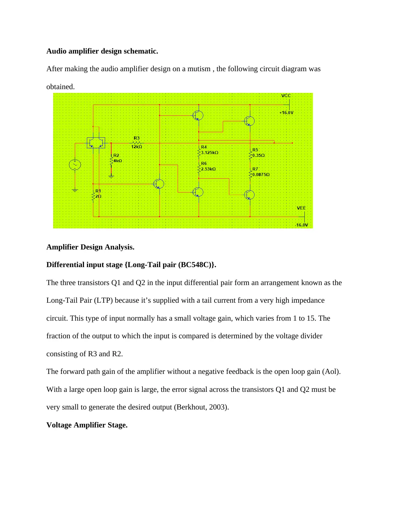
This report details the design of an audio amplifier using a bipolar transistor long-tail pair input stage and a 1W BJT class-AB complementary output stage, intended to drive an 8-ohm speaker with discrete transistors. The design adheres to specifications including a minimum voltage gain of 1500 and compliance with a +16V supply rail. The report covers the design process, component selection (BC817, BC807, BC548C), theoretical calculations for resistor values and voltage gains, DC analysis, and simulation results obtained using Multisim. The amplifier's performance is analyzed, discrepancies between simulated and calculated values are discussed, and the overall functionality and efficiency of the class AB amplifier are evaluated, highlighting its advantages in terms of efficiency, linearity, and low crossover distortion. The report concludes with a summary of the design process and results, supported by datasheets, schematics, and relevant bibliography.

1 out of 13
Related Documents


Your All-in-One AI-Powered Toolkit for Academic Success.
+13062052269
info@desklib.com
Available 24*7 on WhatsApp / Email
![[object Object]](/_next/static/media/star-bottom.7253800d.svg)
Copyright © 2020–2026 A2Z Services. All Rights Reserved. Developed and managed by ZUCOL.