UTHM Project: Monitoring and Controlling Power of EDFA C Band
VerifiedAdded on 2023/06/04
|10
|1665
|299
Project
AI Summary
This project details the monitoring and control of power in a C band Erbium Doped Fiber Amplifier (EDFA) using an Arduino microcontroller. The project aims to enhance optical communication by understanding the operation and applications of microcontrollers in controlling fiber optic amplifiers. Key ...
CE 2.1 Project Information
Name of the project: Monitoring and Controlling power of C Band Erbium Doped
Fiber Amplifier (EDFA)
Location of the project: Please fill
Project Duration: Please fill
Organization: Please fill
Role and Designation during the time: Project Developer
CE 2.2 Project Background
CE 2.2.1 Characteristics of the project
The EDFA or the erbium doped fiber amplifier is the specific device, which could
subsequently amplify the several optical signals and is used for boosting the input optical
signals through a fiber optic communications system. During this project, I had to monitor
and control the power of EDFA for the purpose of allowing easy control of power. I noted
that the most significant point about this EDFA is its high gain and noise figure. Generally,
there are several designs of EDFA, however, I selected Gain Control in C band EDFAs. I
have used Arduino microcontroller to control my EDFA and also ensure that the signal is of
high gain. This was one of the most important projects in electronics engineering career, as I
had to control the power by changing the laser diode power. I limited the range of C band in
EDFA between 1530nm to 1560nm. For configuring this EDFA, I undertook wavelength
combinations of 980/1550nm for coupling the signal optical and pump power.
Paraphrase This Document
Need a fresh take? Get an instant paraphrase of this document with our AI Paraphraser
CE 2.2.2 Objectives developed for the project
The optical amplifiers amplify the signals directly and convert electrical signals to
light energy by a laser diode. I had to monitor as well as control the power of C band in
EDFA. I wanted to provide a better optical communication by understanding the operation
and applications of microcontroller to control the operations of fiber optic amplifier. For
completing this project, I developed the following objectives:
To monitor as well as control the total power of C band erbium doped fiber amplifier.
To utilize the Arduino microcontroller for controlling the EDFA and providing
efficiency.
To identify the existing flaws or faults within the erbium doped fiber amplifier and try
to eradicate them.
To obtain signal with high gain.
To compare the obtained results with the theoretical value to note whether the
obtained results are accurate or not.
To use OptiSystem 12.0 simulating program for simulating the project.
CE 2.2.3 My area of work
As an electronics and communication engineer by profession, I was appointed as the
project developer in this project by my project supervisor. This is mainly because I had
worked in several significant electronics projects in my career and had the ability of
executing a project alone. During my education, I had keen interest in power control, circuit
designing as well as power generation. These three were highly required in this project and
thus I was the project developer, for not only monitoring the power of EDFA but also
assisting my project supervisor. I was selected as I had knowledge to use OptiSystem 12.0
simulating program to simulate the project.
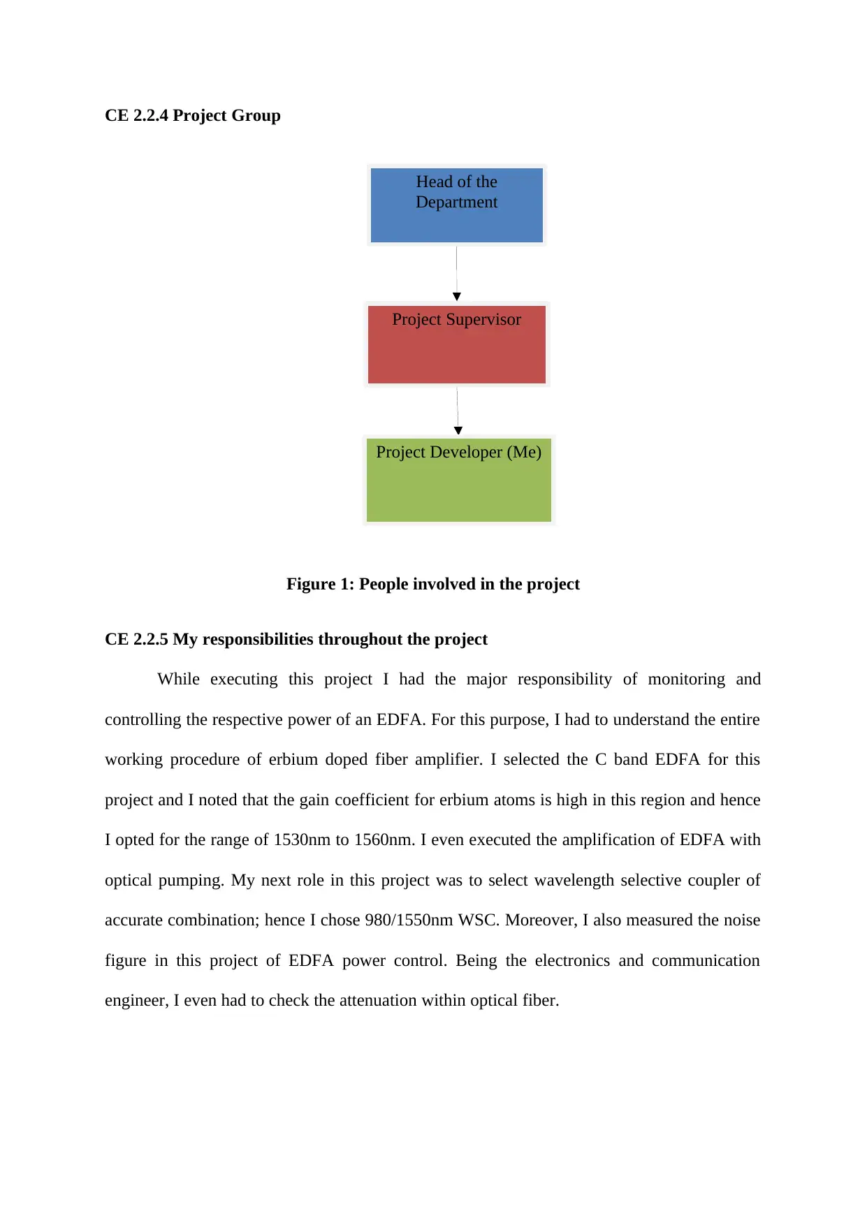
Head of the
Department
Project Supervisor
Project Developer (Me)
CE 2.2.4 Project Group
Figure 1: People involved in the project
CE 2.2.5 My responsibilities throughout the project
While executing this project I had the major responsibility of monitoring and
controlling the respective power of an EDFA. For this purpose, I had to understand the entire
working procedure of erbium doped fiber amplifier. I selected the C band EDFA for this
project and I noted that the gain coefficient for erbium atoms is high in this region and hence
I opted for the range of 1530nm to 1560nm. I even executed the amplification of EDFA with
optical pumping. My next role in this project was to select wavelength selective coupler of
accurate combination; hence I chose 980/1550nm WSC. Moreover, I also measured the noise
figure in this project of EDFA power control. Being the electronics and communication
engineer, I even had to check the attenuation within optical fiber.
You're viewing a preview
Unlock full access by subscribing today!
CE 2.3 Distinctive Activity
CE 2.3.1 Comprehending the Theory of Project
The optical fiber amplifiers use optical pumping and in this project, I have used
photons to directly raise electrons into excited states. I triggered the excited electrons into
stimulated emission and a new photon was released. I have used tap couplers of 99:1 for
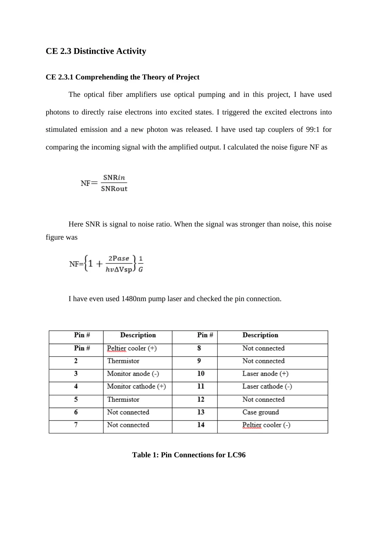
comparing the incoming signal with the amplified output. I calculated the noise figure NF as
Here SNR is signal to noise ratio. When the signal was stronger than noise, this noise
figure was
I have even used 1480nm pump laser and checked the pin connection.
Table 1: Pin Connections for LC96
Paraphrase This Document
Need a fresh take? Get an instant paraphrase of this document with our AI Paraphraser
CE 2.3.2 Engineering knowledge and skills applied in the project
To complete the project, I had used theoretical knowledge of power analysis and
signals along with the simulation techniques that are done by Optisystem 12.0 program.
Within methodology segment, I have used my knowledge power consumption and current
calculation depending on my circuit structure. I even used my knowledge of laser diode and
photodiode for making a proper connection. The connection between laser diode and
photodiode was set up in laser diode pump. For software development, I have used C
programming language.
CE 2.3.3 Accomplishment and Task Performed
I have used my electronics engineering knowledge for monitoring and controlling
EDFA power. I checked that the input and output tap coupler divide the received optical
signal at a predetermined ration on X: Y, where X=10% and Y=90%. With the help of
Arduino microcontroller, I monitored the input power, output power and gain.
I even used OptiSystem 12.0 simulation program for simulating the project. The entire
project is subdivided into four stages like researching about EDFA, combining project design
as well as simulating the EDFA, software development with C program and finally
completing the experiments for EDFA power monitor and control.
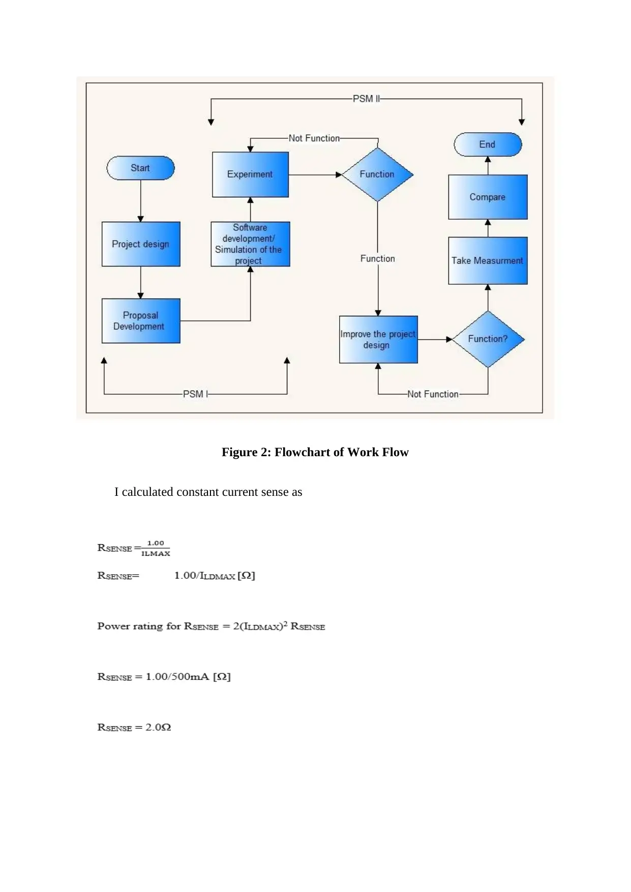
Figure 2: Flowchart of Work Flow
I calculated constant current sense as
I calculated constant current sense as
You're viewing a preview
Unlock full access by subscribing today!
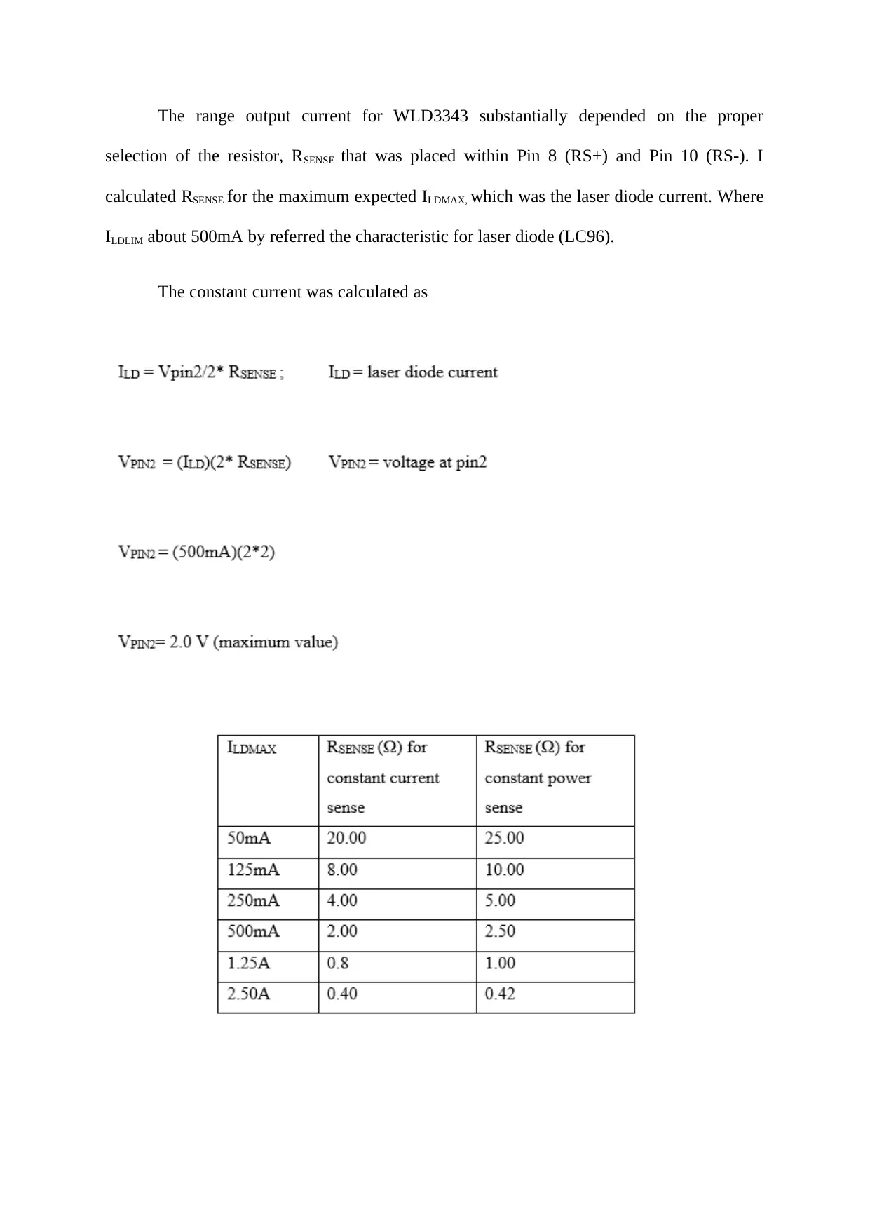
The range output current for WLD3343 substantially depended on the proper
selection of the resistor, RSENSE that was placed within Pin 8 (RS+) and Pin 10 (RS-). I
calculated RSENSE for the maximum expected ILDMAX, which was the laser diode current. Where
ILDLIM about 500mA by referred the characteristic for laser diode (LC96).
The constant current was calculated as
selection of the resistor, RSENSE that was placed within Pin 8 (RS+) and Pin 10 (RS-). I
calculated RSENSE for the maximum expected ILDMAX, which was the laser diode current. Where
ILDLIM about 500mA by referred the characteristic for laser diode (LC96).
The constant current was calculated as
Paraphrase This Document
Need a fresh take? Get an instant paraphrase of this document with our AI Paraphraser
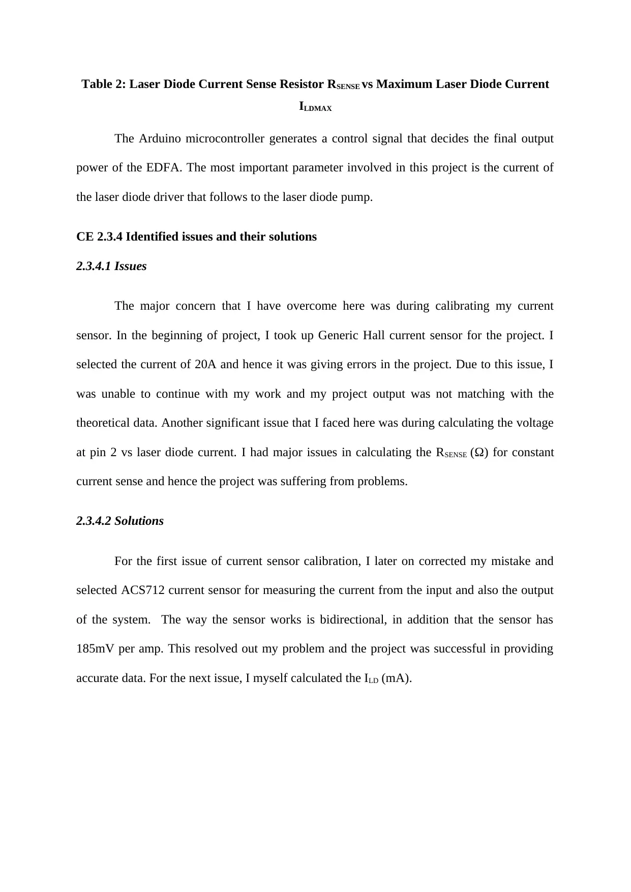
Table 2: Laser Diode Current Sense Resistor RSENSE vs Maximum Laser Diode Current
ILDMAX
The Arduino microcontroller generates a control signal that decides the final output
power of the EDFA. The most important parameter involved in this project is the current of
the laser diode driver that follows to the laser diode pump.
CE 2.3.4 Identified issues and their solutions
2.3.4.1 Issues
The major concern that I have overcome here was during calibrating my current
sensor. In the beginning of project, I took up Generic Hall current sensor for the project. I
selected the current of 20A and hence it was giving errors in the project. Due to this issue, I
was unable to continue with my work and my project output was not matching with the
theoretical data. Another significant issue that I faced here was during calculating the voltage
at pin 2 vs laser diode current. I had major issues in calculating the RSENSE (Ω) for constant
current sense and hence the project was suffering from problems.
2.3.4.2 Solutions
For the first issue of current sensor calibration, I later on corrected my mistake and
selected ACS712 current sensor for measuring the current from the input and also the output
of the system. The way the sensor works is bidirectional, in addition that the sensor has
185mV per amp. This resolved out my problem and the project was successful in providing
accurate data. For the next issue, I myself calculated the ILD (mA).

Table 3: Voltage at Pin 2 vs Laser Diode Current
CE 2.3.5 Plan to produce creative and innovative work
For properly executing this project, I have made an important plan for producing the
most creative as well as innovative work. Since, I am an electronics engineer, I paid extra
attention to the circuit designing and power monitoring or control. I have taken continuous
follow ups to ensure that I would get perfect results.
CE 2.3.6 Collaborative Work
I have executed this project completely alone with my supervisor who had helped in
my entire project work. I had met him consistently and provided a weekly presentation about
the desired data for this project. I required increasing my knowledge for the calculation work
and even required acquiring core programming knowledge of C to complete software
development. In the final week, I and supervisor met out HOD, who was quite happy with my
project.
You're viewing a preview
Unlock full access by subscribing today!

CE 2.4 Project Review
CE 2.4.1 Project Overview
The main purpose of this project was monitoring and controlling the respective power
of C band EDFA with proper efficiency. Moreover, Arduino microcontroller was used for the
hardware parts and OptiSystem 12.0 simulation program was used for software part. The
results were calculated and compared with the desired outputs.
CE 2.4.2 My Contribution to work
I was assigned as the developer of project in this particular project and I have
successfully accomplished every work that had led to the proper project deployment. I even
had to determine the outline as well as project flow chart to understand the progress.
1 out of 10
Related Documents
Your All-in-One AI-Powered Toolkit for Academic Success.
+13062052269
info@desklib.com
Available 24*7 on WhatsApp / Email
![[object Object]](/_next/static/media/star-bottom.7253800d.svg)
Unlock your academic potential
© 2024 | Zucol Services PVT LTD | All rights reserved.


