Report: Analysis and Design of Passive RC and LC Low Pass Filters

Verified

Added on  2022/09/07

|18
|1738
|43
Practical Assignment
AI Summary
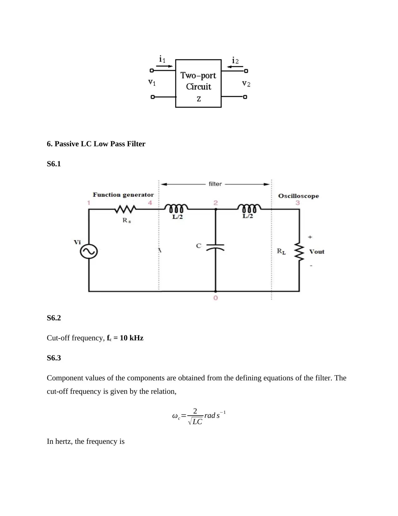
This assignment analyzes both RC and LC low pass filters, detailing their design, operation, and performance characteristics. The solution includes circuit diagrams, component values, and experimental results obtained through Multisim simulations. It covers the calculation of cutoff frequencies, transfer functions, and two-port network representations for each filter type. The report presents tables of results, graphical measurements, and derivations of transfer functions, including the impact of source and load resistances. Furthermore, it compares the theoretical and experimental results, discusses potential sources of error, and highlights the order of the filters. The analysis includes a comparison of the phase shifts at the cutoff frequencies for both filter types, and concludes with a discussion of the key findings and their implications.
Document Page
S5.1 Circuit Diagram
S5.2
Output impedance of the function generator, RS = 50Ω
Input impedance of the oscilloscope, RL = 1
S5.3
Cut off frequency, fc = 10 kHz
S5.4
The cut-off frequency of the filter in question is 10 kHz and is given by the equation
f c= 1
2 π Req C
Req takes into account both the source and load resistance. If the value of capacitance (C) is
chosen to be C=0.01 μF, the resistance is approximately
Req = 1
2 π f c C 1.591 k Ω
Thus,
Capacitor, C =0.33 F
Resistance, R 1.591
tabler-icon-diamond-filled.svg

Paraphrase This Document

Need a fresh take? Get an instant paraphrase of this document with our AI Paraphraser
Document Page
S5.5
Find an attached file of the RC circuit as built in multism
S5.6
The preferred standard manufactured values for the capacitor and the resistor are:
Capacitor, C = (10 + 000 +/- 5%) pF = 0.015 % μ F
Resistance, R 16 x 102 5 % Ω=1.6 5 %k Ω
S5.7
Frequency,f
(kHz)
I/P
Volts
Vi
O/P Volts
Vo
Gain G 20 log10 ( V O
V i ) =GdB Phase
O
0.1 0.2 0.2 1 0 -0.85
0.3 0.6 0.6 1 0 -1.78
0.5 0.8 0.8 1 0 -2.97
0.8 1 1 1 0 -4.74
1 1.1 1.1 1 0 -5.94
2 1.5 1.5 1 0 -11.7
4 1.8 1.66 0.9222 -0.70329 -22.5
6 2.2 1.87 0.85 -1.41162 -31.9
8 2.4 1.84 0.7667 -2.30787 -39.6
10 3 2.08 0.6933 -3.18116 -46
20 3.2 1.39 0.4344 -7.2427 -64.2
30 3.6 1.1 0.3056 -10.2982 -72.1
40 4 0.94 0.235 -12.5786 -76.4
50 4.5 0.85 0.1889 -14.4759 -79
90 5 0.54 0.108 -19.3315 -83.9
Document Page
S5.8 & S5.9
Document Page
S5.10 Graph Measurements:
S5.10.1 The cut-off frequency is 10 kHz (as indicated on the graphical plots)
f c
actual=10 kHz
S5.10.2 The per decade slope of the gain magnitude is -20dB/decade (as indicated on the
graphical plots)
Sactual
decade =20 dB /decade
S5.10.3 The per octave slope of the gain magnitude is -6dB/octave (as indicated on the graphical
plots)
Sactual
octave =6 dB /octave
S5.10.4 The pass band phase is between 0 to -45o (as indicated on the graphical plots). In
radians,
1
4 π θactual
pass 0
S5.10.5 The stop band phase is between -45o to -90o (as indicated on the graphical plots). In
radians,
π
2 θactual
stop 1
4 π
S5.10.6 The phase in radians at the cut-off frequency is obtained from the graph as -45o. In
radians,
θactual
cutoff =45
180 π =1
4 π rads
S5.10.7 The cut-off frequency obtained from the graph is 10 kHz and that in design specification
is 10 kHz. Therefore the fractional difference is zero i.e.
Ef =0
tabler-icon-diamond-filled.svg

Paraphrase This Document

Need a fresh take? Get an instant paraphrase of this document with our AI Paraphraser
Document Page
S5.11 Derivation of the transfer function for the filter circuit
From the equivalent circuit diagram in S.5.1, the transfer function is derived as below
The output voltage is obtained by voltage divider rule as,
V out =
( RL
sC
RL + 1
sC )
(Rs + R+
RL
sC
RL+ 1
sC ) V ¿
Simplifying the expression,
V out =
( RL
1+sC RL )
( Rs + R+ RL
1+ sC RL ) V ¿
On re-arranging, the transfer function for the above filter reduces to,
V out
V ¿
= RL
Rs + R+RL+ sC RL( Rs + R)
But the output impedance of the function generator, RS = 50Ω and the input impedance of the
oscilloscope, RL = 1 . Substituting these values in the above expression, the transfer function
becomes,
V out
V ¿
= (1 x 10⁶)
50+ R+(1 x 10⁶ )+(1 x 10⁶)sC (50+ R)
The calculated values of the capacitor (C) and the resistor (R) at the cut-off frequency are 0.01
μ F and 1.6 k Ω respectively. Replacing these values in the transfer function above, the equation
reduces to
H ( s )= V out
V ¿
= 106
1001650+ 16.5 s
Document Page
The above transfer function is in the s-domain. To convert it the complex frequency domain, s is
replaced with . The result is
H ( ) = V out
V ¿
= 106
1001650+ j 16.5 ω
S5.12 Derivation of the two port representation of the circuit
The two port network is defined in terms of Z-parameters. For the given RC network, the Z-
parameters are obtained as follows:
Z11= V 1
I1 |(I ¿¿ 2=0)=Rs + R+ 1
jωC ¿
Z21= V 2
I 1 |( I¿¿ 2=0)= 1
jωC ¿
Z22= V 2
I2 |(I ¿¿ 1=0)= 1
jωC ¿
Z12= V 1
I 2 |(I ¿¿ 1=0)= 1
jωC ¿
For C=0.33 FR=1.591 , Rs=50 Ω
Z11=1.591 x 10³ +50+ 1
j 2 π x 10 x 0.33 x 103 =1641 j 4.82 x 10⁵ Ω
Z12= 1
j 2 π x 10 x 0.33 x 103 = j 4.82 x 10⁵ Ω
Z22= 1
j 2 π x 10 x 0.33 x 103 = j 4.82 x 10⁵ Ω
Z21= 1
j 2 π x 10 x 0.33 x 103 = j 4.82 x 10⁵ Ω
In matrix form, it is
[ Z ]= [ 1641 j 4.82 x 10⁵ j 4.82 x 10⁵
j 4.82 x 10⁵ j 4.82 x 10⁵ ]
Document Page
6. Passive LC Low Pass Filter
S6.1
S6.2
Cut-off frequency, fc = 10 kHz
S6.3
Component values of the components are obtained from the defining equations of the filter. The
cut-off frequency is given by the relation,
ωc= 2
LC rad s1
In hertz, the frequency is
tabler-icon-diamond-filled.svg

Paraphrase This Document

Need a fresh take? Get an instant paraphrase of this document with our AI Paraphraser
Document Page
f c= 1
π LC
If a capacitor value of 0.1 μ F is chosen, the inductor value is
L= ( 1
π f c C )
2
10.13 mH
The matching impedances Rs and RL are therefore obtained as
Rs=RL= L
C 318.28 Ω
Inductor, L = 10.13 mH
Capacitor, C = 0.1 μ F
S6.4
Find an attached file of the LC circuit as built in multism
S6.5
The standard preferred manufacturer’s values are;
L = (10 + 000 +/- 1%) μ H = 10 mH
C = (10 + 0000 +/- 5%) pF = 0.1 5 % μ F
Document Page
S6.6
Table of results
Frequency,f
(kHz)
I/P
Volts
Vi
O/P
Volts
Vo
Gain G 20 log10 ( V O
V i ) =GdB Phase
O
0.1 0.2 0.1 0.5 -6.0206 -1.64
0.3 0.6 0.3 0.5 -6.0206 -3.4
0.5 0.8 0.4 0.5 -6.0206 -5.66
0.8 1 0.5 0.5 -6.0206 -9.06
1 1.1 0.55 0.5 -6.0206 -11.4
2 1.5 0.75 0.5 -6.0206 -22.8
4 1.8 0.9 0.5 -6.0206 -47
6 2.2 1.09 0.49545 -6.0999 -73.9
8 2.4 1.08 0.45 -6.9357 -105
10 3 1.07 0.35667 -8.9547 -136
20 3.2 0.2 0.0625 -24.082 -210
30 3.6 0.07 0.01944 -34.224 -231
Document Page
40 4 0.03 0.0075 -42.499 -241
50 5 0.02 0.004 -47.959 -247
90 14 0.01 0.00071 -62.923 -257
tabler-icon-diamond-filled.svg

Paraphrase This Document

Need a fresh take? Get an instant paraphrase of this document with our AI Paraphraser
Document Page
S6.7 & 6.8
Document Page
S6.9 Graph Measurements:
S6.9.1 The cut-off frequency is 10 kHz (as indicated on the graphical plots)
f c
actual=10 kHz
S6.9.2 The per decade slope of the gain magnitude is -20dB/decade (as indicated on the
graphical plots)
Sactual
decade =20 dB /decade
S6.9.3 The per octave slope of the gain magnitude is -6dB/octave (as indicated on the graphical
plots)
Sactual
octave =6 dB /octave
S6.9.4 The pass band phase is between 0 to -135o i.e. angles greater than -135 degrees (as
indicated on the graphical plots). In radians,
3
4 π θactual
pass 0
S6.9.5 The stop band phase is between -135o to -360o i.e. angles less than 135 degrees (as
indicated on the graphical plots)
2 π θactual
stop 3
4 π
S6.9.6 The phase in radians at the cut-off frequency is obtained from the graph as
θactual
cutoff =135
180 π=3
4 π rads
S6.9.7 The cut-off frequency obtained from the graph is 10 kHz and that in design specification
is 10 kHz. Therefore the fractional difference is zero i.e.
Ef =0
Document Page
S6.10
Let the voltage across the capacitor be V1
By voltage divider rule, this voltage V1 is given as
V 1=
1
s C ¿ ( RL+s L'
)
1
s C ¿ ( RL+ s L' ) +Rs +s L'
V i
¿
( RL+ s L'
s C ( RL+ s L'+ 1
s C ) )
RL+s L'
s C ( RL +s L' + 1
s C ) + Rs + s L'
V i
Simplifying, we have
V 1= RL+s L'
RL+ s L'+ s C (RL+s L'+ 1
s C ) ( Rs +s L' )
V i
But the output voltage, by voltage divider rule, is
V o = RL
RL+ s L' V 1
¿ ( RL
RL+ s L' ) ( RL +s L'
RL +s L' + s C ( RL +s L' + 1
s C ) ( Rs+ s L'
) ) V i
¿ RL
RL+ s L' +s C ( RL+ s L' + 1
s C ) ( Rs+s L' )
V i
tabler-icon-diamond-filled.svg

Paraphrase This Document

Need a fresh take? Get an instant paraphrase of this document with our AI Paraphraser
Document Page
The transfer function of the circuit is defined as the ratio of the output voltage to the input
voltage i.e.
H ( s )= V o
V i
= RL
RL +s L' + s C (RL+s L' + 1
s C ) ( Rs+s L' )
Simplifying the above expression, the transfer function reduces to
H ( s )= V o
V i
= RL
L'2 Cs3 + ( RL L' C+ Rs L' C ) s2+ ( RL Rs C +2 L' ) s+ ( RL+ Rs )
Where,
L' = L
2
Replacing the variables with their equivalent values we have,
H ( s )= 318.28
2.565 x 10¹² s3+3.2242 x 10⁷ s2+0.020 s+636.56
Document Page
S6.11
The two port network is defined in terms of Z-parameters. For the given LC network, the Z-
parameters are obtained as follows:
Z11= V 1
I 1 |(I ¿¿ 2=0)=Rs + jωL
2 + 1
jωC =Rs + j ( ωL
2 1
ωC ) ¿
Z21= V 2
I 1 |( I¿¿ 2=0)= 1
jωC ¿
Z22= V 2
I 2 |(I¿¿ 1=0)= jωL
2 + 1
jωC = j ( ωL
2 1
ωC ) ¿
Z21= V 1
I 2 |(I ¿¿ 1=0)= 1
jωC ¿
For C=0.1 μFL=10.13 mH , Rs =318.28 Ω
Z11=318.28+ j ( 2 π x 10 x 10.13
2 1
2 π x 10 x 0.1 x 103 ) =318.28+ j 159.09 Ω
Z21= 1
j 2 π x 10 x 0.1 x 103 = j159.15 Ω
Z22= j ( 2 π x 10 x 10.13
2 1
2 π x 10 x 0.1 x 103 )= j159.09 Ω
Z12= 1
j 2 π x 10 x 0.1 x 103 = j159.15 Ω
[ Z ]= [ 318.28+ j 159.09 j159.15
j159.15 j159.09 ] Ω
Document Page
S7.1
It was so desired for the cut-off frequency of the low pass filter in question to be 10kHz. Results
obtained from MULTISIM and depicted in graphical plots above give the cut-off frequency as 10
kHz for both the RC and LC circuits. This satisfies the main experimental objective. The dB per
decade and dB per octave slopes obtained are -20 and -6 respectively. This also conforms to the
information in literature. Moreover, the phase at the cut off frequency for the RC low pass filter
is -45 degrees while that of LC low pass filter is -135 degrees – which also agrees with the
theoretical information. In some cases, however, it may not be possible to accurately achieve the
exact results as so desired. Possible deviations may occur in the results obtained from simulation.
Such sources of error can be attributed to;
1. Round-off of the component values to the nearest equivalent manufactured values.
Design equations occasionally yield values of resistors, inductors and capacitors which
are not standard (Uysal & Watkins, 2015). This necessitates for round off of these values
to the nearest manufactured equivalents. Hence, this may contribute to erroneous results
(Huang et al., 2015)
2. Possible round off errors in the simulator when run, as it tries to solve the circuit, to give
the readings of output voltage (Brown, 2019)
3. The chosen values of input and output impedances could be too high or too low (Serra &
Paulino, 2014)
tabler-icon-diamond-filled.svg

Paraphrase This Document

Need a fresh take? Get an instant paraphrase of this document with our AI Paraphraser
Document Page
S7.2
It is observed that the transfer function of the RC low pass filter is of first order. By this, it
implies that the highest power of s in the denominator is unity. It is a first order system because
only two passive elements make up the circuit i.e. a capacitor and resistors. The function
generator provides resistance (Rs); oscilloscope offer load resistance (RL) and the resistor making
up the filter unit also provide resistance (R). Combined effects of all these three sources of
resistances make up the overall resistance of the circuit (Thompson, 2016).
While for LC low pass filter, the highest power of s in the characteristic equation is three making
it a third order or a three pole system. The system is of third order because all the three
passive components are present in the equivalent circuit i.e. there exists an inductor, capacitor
and resistors. The resistors offer resistance for impedance matching in the filter and are modeled
from the function generator and oscilloscope (Nassir, 2017)
The RC low pass filter give a phase of -45o while the LC low pass filter gives a phase of -135o at
the cut off frequency.
Document Page
References
Brown, J. M. (2019). Chapter 2: Classical results of network synthesis. Passive Network
Synthesis: An Approach to Classification, 5-18.
Huang, C., Chen, C., Zhou, M. J., & Wu, J. H. (2015). An active-RC reconfigurable lowpass-
polyphase biquad filter for wireless receiver. Analog Integrated Circuits and Signal
Processing, 84(1), 97-105.
Nassir, H. S. (2017). Basic analysis of resistive circuits. Electric Circuits and Signals, 83-112.
Serra, H. A., & Paulino, N. (2014). Low-pass filter Topologies. SpringerBriefs in Electrical and
Computer Engineering, 15-22.
Thompson, M. T. (2016). Analog low-pass filters. Intuitive Analog Circuit Design, 385-416.
Uysal, S., & Watkins, J. (2015). Novel microstrip low-pass/high-pass directional couplers/filters.
IEEE Proceedings on Southeastcon.
chevron_up_icon
1 out of 18
circle_padding
hide_on_mobile
zoom_out_icon
[object Object]