Competency Demonstration Report: Microstrip Antenna Design Project
VerifiedAdded on 2020/04/01
|9
|1705
|44
Report
AI Summary
This document presents a Competency Demonstration Report (CDR) detailing a project focused on the design and implementation of a microstrip patch antenna for broadband indoor wireless systems. The report outlines the project's background, aims, and objectives, emphasizing the developme...

Competency
Demonstration Report
(CDR)
Career Episode 3
Demonstration Report
(CDR)
Career Episode 3
Paraphrase This Document
Need a fresh take? Get an instant paraphrase of this document with our AI Paraphraser
CE 3.1: Introduction to the Undertaken Project
Name of the Project : Design a Micro-strip Patch Antennas for Broadband
Indoor Wireless Systems
Geographical Location : [Please Fill]
Project Duration : [Please Fill]
Organization : [Please Fill]
Position in the Project : Team Leader
CE 3.2. Background of the Telecommunication Project
CE 3.2.1: Features of the Undertaken Project
With the exponential rise of Technology various household devices are connected with
WiFi including video game console, computers, digital audio player and smartphone. The
integration of Wi-Fi allows the devices to wirelessly connect to the Internet network. The
application of Wi-Fi allows the interconnection between the devices through or access point
within a smaller area to a larger area like square miles. In addition to that I have observed that
the development in the Semiconductor devices has focused on the implementation of antenna
using microstrip. Therefore, I took this project for the development of low cost microstrip patch
antenna for ensuring wireless communication. I have used dielectric substrate for the antenna and
conducting material including gold and copper for developing the radiator of the antenna. During
the implementation of the project I have focused on delivering low cost lightweight easy
Page 1 of 9
fabrication and simple design of the antenna on curved surface. I have further focused on
enhancing the functionality and effectiveness of the antenna while reducing the impact of narrow
impedance bandwidth.
CE 3.2.2: Aims and Objectives
In this project I have focused on developing the most simple form of microstrip antenna
for wireless communication. Therefore I have proposed on implementing a radiating patch over
the dielectric substrate on each side and grounding the plane on the other. I have further focused
on developing the page with a good conductor material like gold or copper in in shape. For the
proper design and implementation of the antenna I have divided the project work into three
major divisions. Apart from that for the easy implementation and proper management of the
project progress I have identified several objective as discussed in the section below.
To identify the appropriate methodology need to be adopted for design of microstrip
antenna;
To Evaluate the appropriate characteristics and specification of the proposed antenna.
To determine the working principle of the microstrip patch antenna.
To conduct the analysis and simulation of the proposed prototype model of the
microstrip patch antenna for indoor application.
CE 3.2.3: Characteristic of my work in the Undertaken Project
I have considered and surveyed different papers, articles and books for recognizing the
characteristics and elements affecting the execution and implementation process of indoor
micros strip patch antenna devices. In addition to that I have developed the appropriate design of
the antenna using dielectric substrate. Moreover, being associated in this project as a team leader
Page 2 of 9
⊘ This is a preview!⊘
Do you want full access?
Subscribe today to unlock all pages.

Trusted by 1+ million students worldwide
I have developed the appropriate plan and schedule for hardware implementation and simulation
of the microstrip patch antenna structure. In addition to that I have reviewed and analyse the
technical knowledge and skill of the team members and subdivided and distributed the workload
among them based on their skill set.
CE 3.2.4: Organizational Structure Associated with this Project
Figure 1: Team Member Associated with the Project
CE 3.2.5: Responsibilities Undertaken by me
I was actively involved for the development of the antenna design and planning for the
project progress. In addition to that, due to my past experience in the field of electronics and
telecommunication, I took more responsibility in developing the prototype model for the micro-
strip antenna. I have further developed the transmission line modeling structure for representing
the microstrip antenna. Apart from that, I have used my knowledge for using SuperNEC
Page 3 of 9
Paraphrase This Document
Need a fresh take? Get an instant paraphrase of this document with our AI Paraphraser
Software system for conducting the simulation of the developed antenna using Method of
Moments package.
CE 3.3: Distinctive Engineering Activity
CE 3.3.1: Theory and Vital Components of the Project
During my work in this project, I have focused myself for the design and implementation
of a low cost and effective micro strip path antenna system that can be used for wireless
communication between nodes. For the design of the antenna, I have used radiating path and
developed with a substrate of dielectric in nature. I have taken rectangular shape of copper as the
required dielectric substrate. The application of copper has allowed me to develop a low cost and
light weight antenna. I have further used the rectangular copper substrate in the main radiator
area. Moreover, in this project, the development of the micro strip antenna has provided with
planer, smaller shape and simplistic structural antenna that made allowed me to apply the
antenna in variable types of devices. I have designed the wireless antenna system to be operated
at 2.4 GHz of frequency and having the gain of 11 dB in indoor application area. In addition to
that, I have also included wide angle beam for the required radiation pattern for improving the
efficiency.
Page 4 of 9
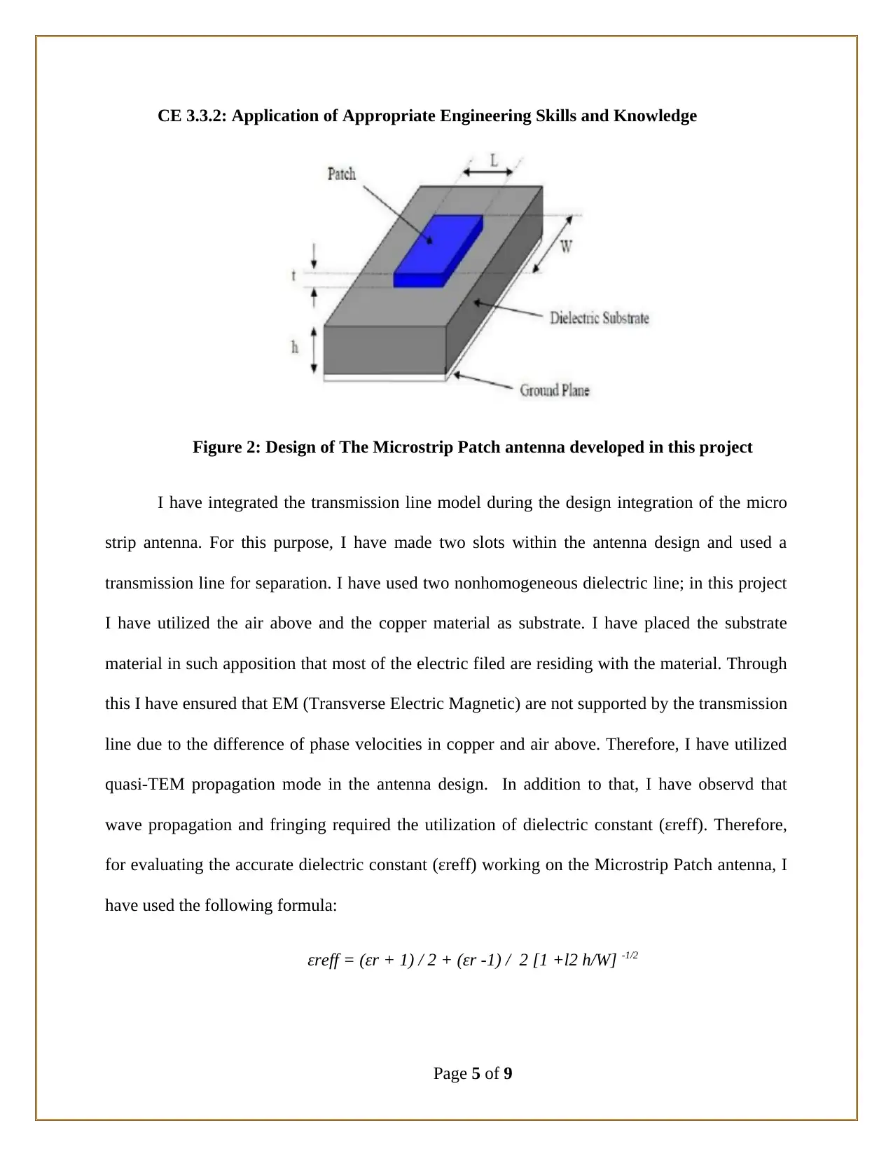
CE 3.3.2: Application of Appropriate Engineering Skills and Knowledge
Figure 2: Design of The Microstrip Patch antenna developed in this project
I have integrated the transmission line model during the design integration of the micro
strip antenna. For this purpose, I have made two slots within the antenna design and used a
transmission line for separation. I have used two nonhomogeneous dielectric line; in this project
I have utilized the air above and the copper material as substrate. I have placed the substrate
material in such apposition that most of the electric filed are residing with the material. Through
this I have ensured that EM (Transverse Electric Magnetic) are not supported by the transmission
line due to the difference of phase velocities in copper and air above. Therefore, I have utilized
quasi-TEM propagation mode in the antenna design. In addition to that, I have observd that
wave propagation and fringing required the utilization of dielectric constant (εreff). Therefore,
for evaluating the accurate dielectric constant (εreff) working on the Microstrip Patch antenna, I
have used the following formula:
εreff = (εr + 1) / 2 + (εr -1) / 2 [1 +l2 h/W] -1/2
Page 5 of 9
⊘ This is a preview!⊘
Do you want full access?
Subscribe today to unlock all pages.

Trusted by 1+ million students worldwide
In the above formual, I have used w for representing the patch width, h for representing
the substrate height, εr for representing the dielectric constant of comer and εreff for defining the
dielectric constant.
CE 3.3.3: Task Accomplishment and Delegation
After development of the hardware model for the microstrip antenna, I had involved
myself with the analysis of the design specification for the antenna. During the design of the
antenna, I have ensured three significant parameter for the antenna including operational
frequency, dielectric constant for substrate and substrate height for the antenna.
CE 3.3.4: Technical Problem and Difficulties Faced
Issue: In the initial model of the antenna design, I have used the specified characteristic
of the dielectric substrate and electromagnetic filed as reference. I have faced significant issue
when the developed specification failed to provide enhanced performance of the antenna design.
Solution: In order to enhance the antenna performance and mitigate the issue I have made
a significant tradeoff between the performance and the antenna dimension. Therefore, I have
selected a thin dielectric substrate with minimum dielectric constant. Through this, I was able to
reduce to size and enhance the efficiency and reduce the power loss of the antenna.
CE 3.3.5: Creative Work Strategies
I have applied my knowledge of using the software model of 4NEC2X and SuperNEC for
producing creativeness in the project. With the use of SuperNEC I was able to include the
Moments electromagnetic method during the simulation of the antenna. I have further developed
an 3D module for the easy user interface and multi level assemblies of the model creation and
Page 6 of 9
Paraphrase This Document
Need a fresh take? Get an instant paraphrase of this document with our AI Paraphraser
the structural input for the antenna. In addition to that, I have prepared efficiency plots, coupling
plots, network analyzers and pattern plots for the developed antenna design. Moreover, with the
application of 4NEC2, I was able to checking, optimizing and geometric structure of the antenna.
Apart from that, I have developed the antenna modeler, and compared the radiation patter for
both far and near field of the designed micro strip antenna.
CE 3.3.6: Team Work Done
In this project, I have focused on delivering the project on time with the use team work
and collaboration among the team members. I have therefore presented the antenna
implementation plan and allocated appropriate resources and team members for proper
management.
CE 3.4: Summary of Project
CE 3.4.1: Overall view of the Undertaken Project
In this project, I was successful in accomplishing the manufacturing and designing the
appropriate specification for the microstrip antenna. From the proper implementation and
analysis of the antenna, I have observed that gain of the developed antenna was 15 dB with
omnidirectional antenna for the indoor applications. In addition to that, I have identified that he
40 degree half beam width is observed for the indoor area of operation.
CE 3.4.2: My Personal Contribution to Project Activities
Throughout the planning phase, I have taken entire initiative in carrying out the research
for identification of the low cost hardware elements for the micro strip communication system.
In addition to that, from my past studies and project experience I have gained intensive
Page 7 of 9

knowledge and information about the implementation of the telecommunication system. I have
used those knowledge in this project for guiding the project team and developing an exceptional
antenna design for the wireless communication.
Page 8 of 9
used those knowledge in this project for guiding the project team and developing an exceptional
antenna design for the wireless communication.
Page 8 of 9
⊘ This is a preview!⊘
Do you want full access?
Subscribe today to unlock all pages.

Trusted by 1+ million students worldwide
1 out of 9
Related Documents
Your All-in-One AI-Powered Toolkit for Academic Success.
+13062052269
info@desklib.com
Available 24*7 on WhatsApp / Email
![[object Object]](/_next/static/media/star-bottom.7253800d.svg)
Unlock your academic potential
© 2024 | Zucol Services PVT LTD | All rights reserved.


