Digital Electronics Laboratory Assignment - FEEE Module Solution

Verified

Added on  2022/08/25

|6
|816
|26
Homework Assignment
AI Summary
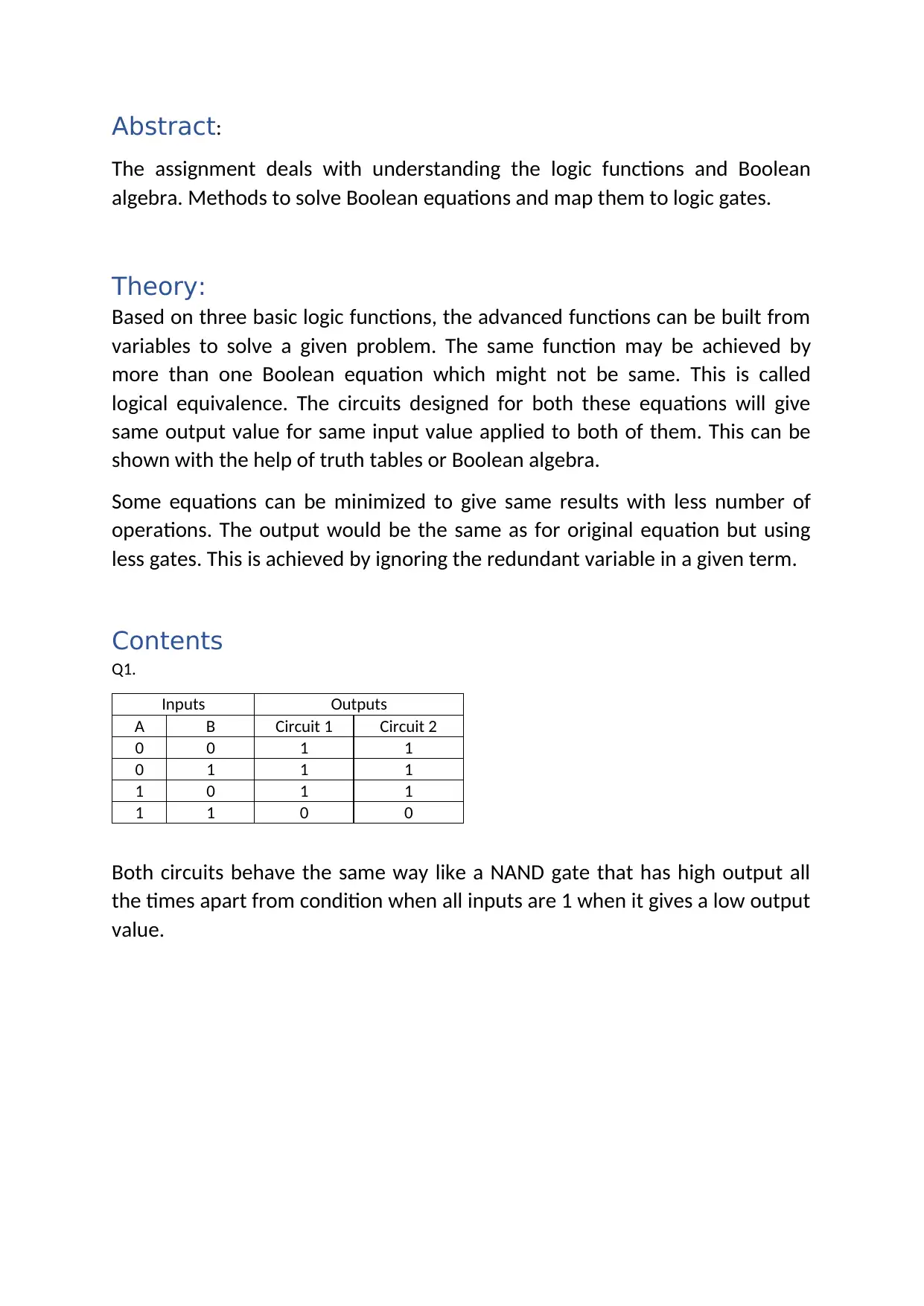
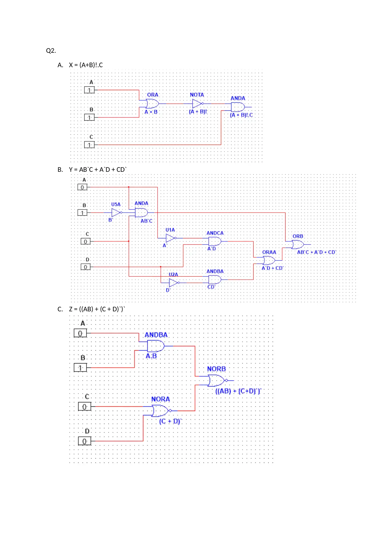
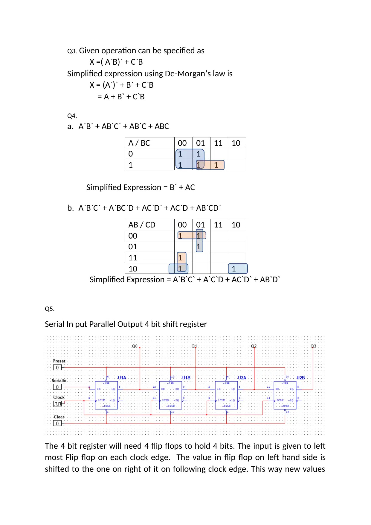
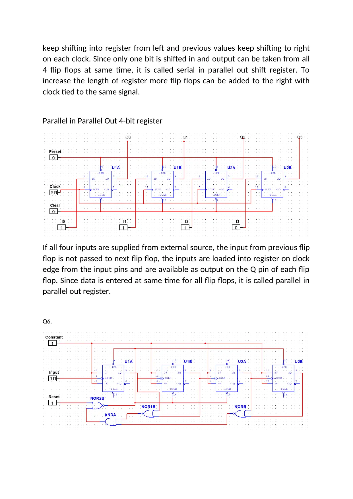
This assignment solution covers fundamental concepts in digital electronics, including logic functions, Boolean algebra, and circuit design. The solution addresses several key areas, starting with the analysis of logic gate behavior, demonstrating logical equivalence through truth tables and Boolean algebra. The assignment then delves into simplifying Boolean expressions using techniques like De Morgan's law and Karnaugh maps. Furthermore, the solution explores the design and operation of shift registers, specifically serial-in parallel-out and parallel-in parallel-out configurations. Finally, the assignment concludes with an examination of module counters, illustrating their functionality and implementation using JK flip-flops and reset mechanisms. The solution provides a comprehensive understanding of digital circuit design principles.
Document Page
Fundamentals of Electrical and Electronic Engineering
Digital Electronics Laboratory Assignment
Submitted By:-
tabler-icon-diamond-filled.svg

Paraphrase This Document

Need a fresh take? Get an instant paraphrase of this document with our AI Paraphraser
Document Page
Abstract:
The assignment deals with understanding the logic functions and Boolean
algebra. Methods to solve Boolean equations and map them to logic gates.
Theory:
Based on three basic logic functions, the advanced functions can be built from
variables to solve a given problem. The same function may be achieved by
more than one Boolean equation which might not be same. This is called
logical equivalence. The circuits designed for both these equations will give
same output value for same input value applied to both of them. This can be
shown with the help of truth tables or Boolean algebra.
Some equations can be minimized to give same results with less number of
operations. The output would be the same as for original equation but using
less gates. This is achieved by ignoring the redundant variable in a given term.
Contents
Q1.
Inputs Outputs
A B Circuit 1 Circuit 2
0 0 1 1
0 1 1 1
1 0 1 1
1 1 0 0
Both circuits behave the same way like a NAND gate that has high output all
the times apart from condition when all inputs are 1 when it gives a low output
value.
Document Page
Q2.
A. X = (A+B)!.C
B. Y = AB`C + A`D + CD`
C. Z = ((AB) + (C + D)`)`
Document Page
Q3. Given operation can be specified as
X =( A`B)` + C`B
Simplified expression using De-Morgan’s law is
X = (A`)` + B` + C`B
= A + B` + C`B
Q4.
a. A`B` + AB`C` + AB`C + ABC
A / BC 00 01 11 10
0 1 1
1 1 1 1
Simplified Expression = B` + AC
b. A`B`C` + A`BC`D + AC`D` + AC`D + AB`CD`
AB / CD 00 01 11 10
00 1 1
01 1
11 1
10 1 1
Simplified Expression = A`B`C` + A`C`D + AC`D` + AB`D`
Q5.
Serial In put Parallel Output 4 bit shift register
The 4 bit register will need 4 flip flops to hold 4 bits. The input is given to left
most Flip flop on each clock edge. The value in flip flop on left hand side is
shifted to the one on right of it on following clock edge. This way new values
tabler-icon-diamond-filled.svg

Paraphrase This Document

Need a fresh take? Get an instant paraphrase of this document with our AI Paraphraser
Document Page
keep shifting into register from left and previous values keep shifting to right
on each clock. Since only one bit is shifted in and output can be taken from all
4 flip flops at same time, it is called serial in parallel out shift register. To
increase the length of register more flip flops can be added to the right with
clock tied to the same signal.
Parallel in Parallel Out 4-bit register
If all four inputs are supplied from external source, the input from previous flip
flop is not passed to next flip flop, the inputs are loaded into register on clock
edge from the input pins and are available as output on the Q pin of each flip
flop. Since data is entered at same time for all flip flops, it is called parallel in
parallel out register.
Q6.
Document Page
Module counter uses Q pin of previous stage as clock of the next stage. Each
time the previous stage output toggles from 1 to 0, the next stage toggles it’s
value. The Constant 1 makes JK flip flops toggle on each input neg edge of
clock. Reset signal sets Preset to 0 and Clear to 0 causing output of flipflop to
be set to 9, the default value. On each input pulse, the counter down counts by
1. Once it reaches the count of 0, the AND gate asserts high input causing
another reset to be asserted. The counter resets to 9 and starts counting again.
Conclusion:
The digital circuits can be broadly divided into sequential and combination
circuits. Both are used for different purposes and most often together to form
a functional unit in a larger circuit. Digital circuits make it possible to design a
well-defined machine that can operate on basis of given input and generate
required outputs without much intervention.
chevron_up_icon
1 out of 6
circle_padding
hide_on_mobile
zoom_out_icon
[object Object]