Ask a question from expert

Ask now

Interconnecting of Design Subsystem Assignment

14 Pages357 Words185 Views
   

Added on  2020-04-13

Interconnecting of Design Subsystem Assignment

   Added on 2020-04-13

BookmarkShareRelated Documents
FPGA SOURCE FILES
Interconnecting of Design Subsystem Assignment_1
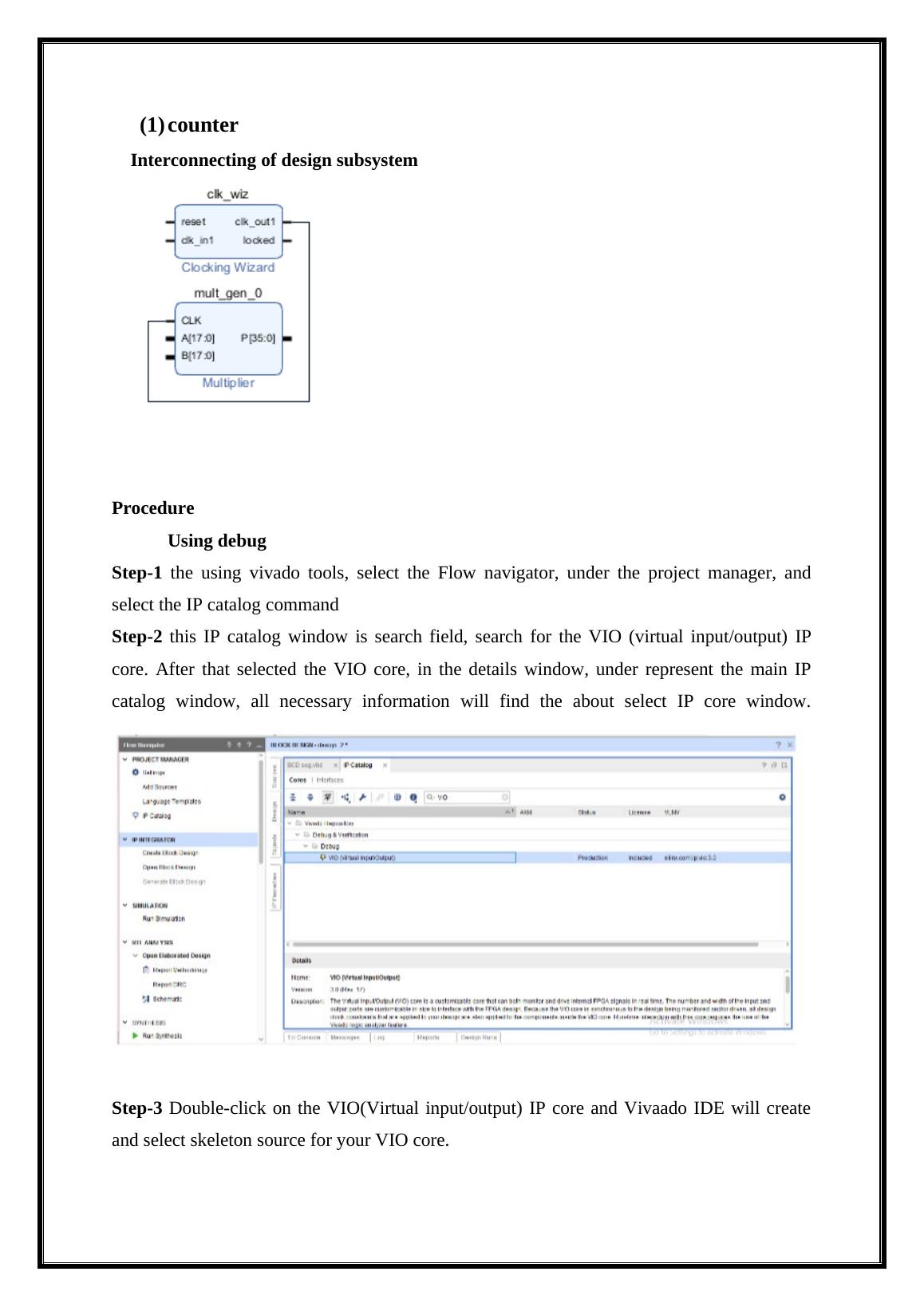
(1)counter Interconnecting of design subsystemProcedureUsing debug Step-1 the using vivado tools, select the Flow navigator, under the project manager, andselect the IP catalog commandStep-2 this IP catalog window is search field, search for the VIO (virtual input/output) IPcore. After that selected the VIO core, in the details window, under represent the main IP
Interconnecting of Design Subsystem Assignment_2
catalog window, all necessary information will find the about select IP core window.Step-3 Double-click on the VIO(Virtual input/output) IP core and Vivaado IDE will createand select skeleton source for your VIO core.
Interconnecting of Design Subsystem Assignment_3
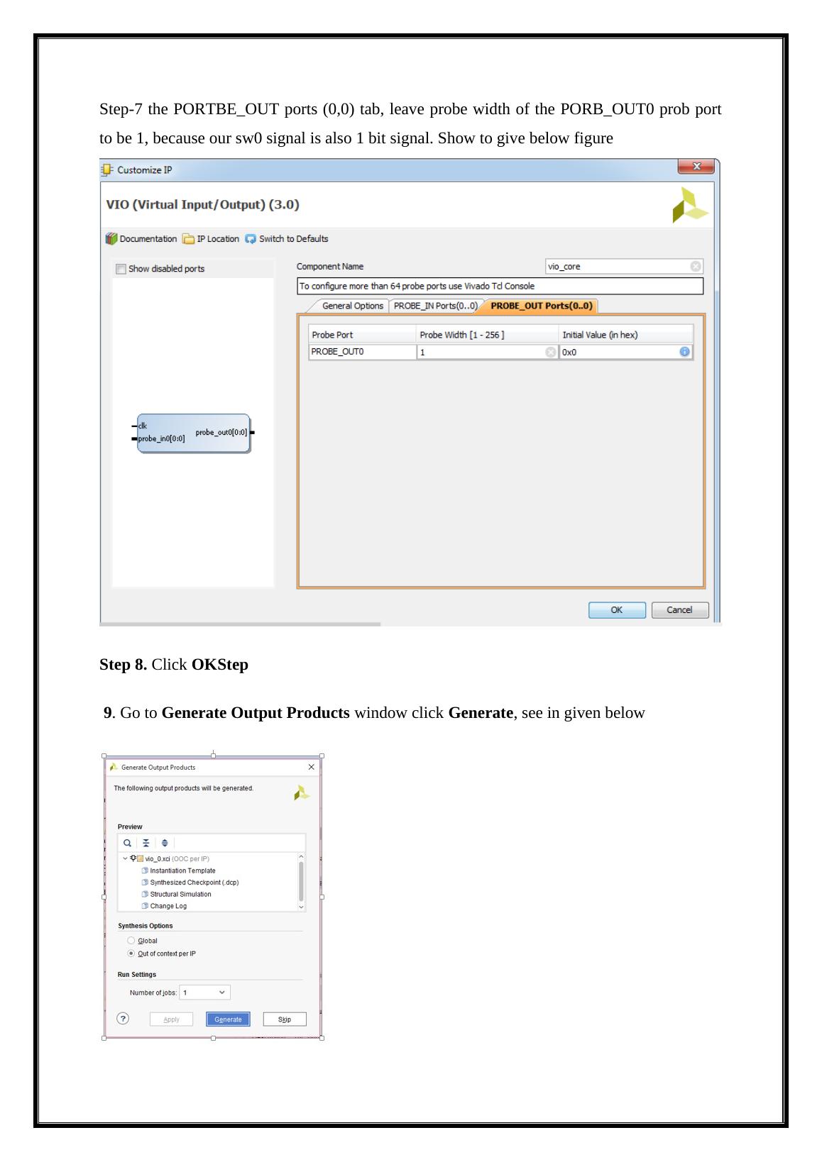
Step-4 using this VIO (input/output) window enter in vio, core name (vio core) in thecomponent name field,Step-5 go to general option tab and select the input probe count to be 1 and output probecount also to be 1,because the input probe for pwm out signal and one outut probe for sw()signal Step-6 this PROBE_IN ports (0, 0) tab leave the probe width of the PROBE_INO probe portto be 1, because our pwm out signal.
Interconnecting of Design Subsystem Assignment_4

End of preview

Want to access all the pages? Upload your documents or become a member.