Electronics Study Material
Added on 2023-04-22
14 Pages1321 Words434 Views
Electronics 1
ELECTRONICS
By Name
Course
Instructor
Institution
Location
Date
ELECTRONICS
By Name
Course
Instructor
Institution
Location
Date
Electronics 2
QUESTION ONE
Given that information vf low pass filter has the following specification;
Fp=2.4 MHz
Fs=MHZ
Lp=3dB
Ls= 40dB
There,
Fp= 2.4 MHz = Ωp=2A*106 = 15.07*106 rad/sec
Fe = 6MHz = ΩA=2A*6*106 = 37.7 *106 rad/sec
Lp= 3dB
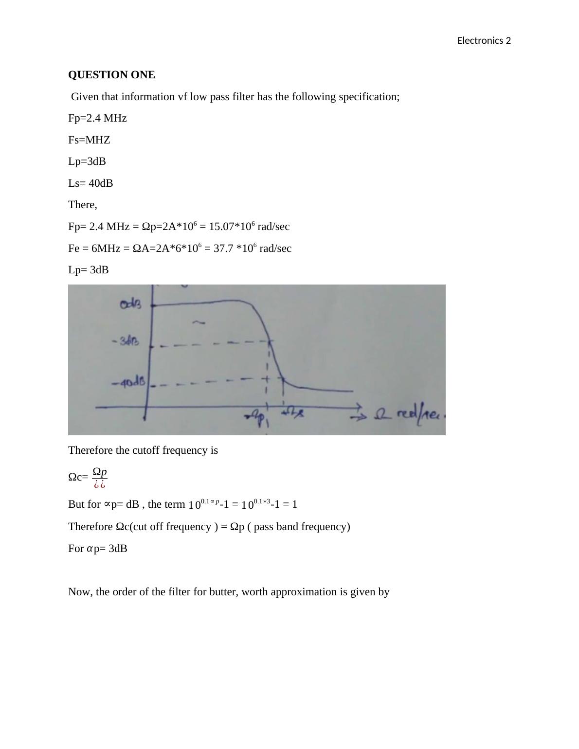
Therefore the cutoff frequency is
Ωc= Ωp
¿ ¿
But for ∝p= dB , the term 1 00.1 ∝ p-1 = 1 00.1∗3-1 = 1
Therefore Ωc(cut off frequency ) = Ωp ( pass band frequency)
For αp= 3dB
Now, the order of the filter for butter, worth approximation is given by
QUESTION ONE
Given that information vf low pass filter has the following specification;
Fp=2.4 MHz
Fs=MHZ
Lp=3dB
Ls= 40dB
There,
Fp= 2.4 MHz = Ωp=2A*106 = 15.07*106 rad/sec
Fe = 6MHz = ΩA=2A*6*106 = 37.7 *106 rad/sec
Lp= 3dB
Therefore the cutoff frequency is
Ωc= Ωp
¿ ¿
But for ∝p= dB , the term 1 00.1 ∝ p-1 = 1 00.1∗3-1 = 1
Therefore Ωc(cut off frequency ) = Ωp ( pass band frequency)
For αp= 3dB
Now, the order of the filter for butter, worth approximation is given by
Electronics 3
N =
log √ 1 00.1 ∝ p−1
1 00.1 ∝ s−1
log ( Ωp
Ωs )
N =
log √ 100.1 ×3−1
1 00.1× 4−1
log ( 15.07 ×1 06
57.6 ×1 06 )
= 5.928
N≈ 6
QUESTION 2
Here, N=6, the characteristics equation is given by
Ga (s) = (s2+0.518s+1)(s2+1.414s+1)(s2+1.432s+1)
Therefore the transfer function of analog prototype filter is given by (NAIR, 2014).
Ha(s)= 1
Ga(s)
( Prototype : A low pass filter with Ωc= 1rad/sec
Ha (s) = 1
(S2 +0518+1)(S2 +1.414 S+1)¿ ¿
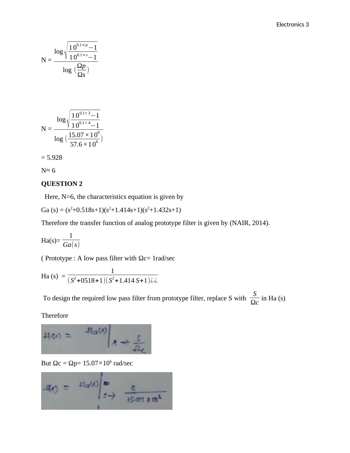
To design the required low pass filter from prototype filter, replace S with S
Ωc in Ha (s)
Therefore
But Ωc = Ωp= 15.07×10⁶ rad/sec
N =
log √ 1 00.1 ∝ p−1
1 00.1 ∝ s−1
log ( Ωp
Ωs )
N =
log √ 100.1 ×3−1
1 00.1× 4−1
log ( 15.07 ×1 06
57.6 ×1 06 )
= 5.928
N≈ 6
QUESTION 2
Here, N=6, the characteristics equation is given by
Ga (s) = (s2+0.518s+1)(s2+1.414s+1)(s2+1.432s+1)
Therefore the transfer function of analog prototype filter is given by (NAIR, 2014).
Ha(s)= 1
Ga(s)
( Prototype : A low pass filter with Ωc= 1rad/sec
Ha (s) = 1
(S2 +0518+1)(S2 +1.414 S+1)¿ ¿
To design the required low pass filter from prototype filter, replace S with S
Ωc in Ha (s)
Therefore
But Ωc = Ωp= 15.07×10⁶ rad/sec
Electronics 4
QUESTION THREE
Given that wn = 4rad/sec
Ɛ=0.5
Wr=? For maximum peak (1 1+(5+w)
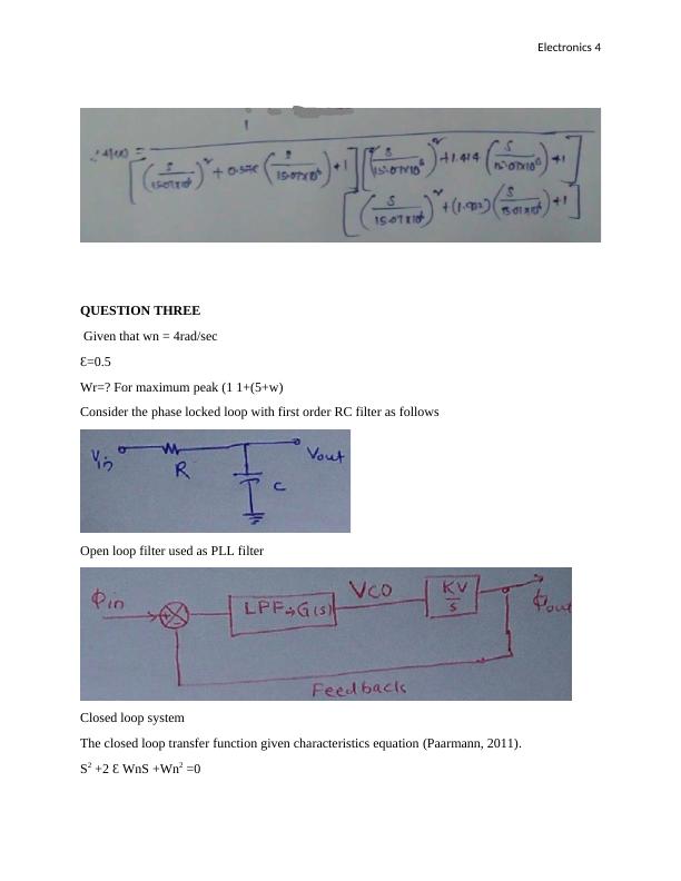
Consider the phase locked loop with first order RC filter as follows
Open loop filter used as PLL filter
Closed loop system
The closed loop transfer function given characteristics equation (Paarmann, 2011).
S2 +2 Ɛ WnS +Wn2 =0
QUESTION THREE
Given that wn = 4rad/sec
Ɛ=0.5
Wr=? For maximum peak (1 1+(5+w)
Consider the phase locked loop with first order RC filter as follows
Open loop filter used as PLL filter
Closed loop system
The closed loop transfer function given characteristics equation (Paarmann, 2011).
S2 +2 Ɛ WnS +Wn2 =0
End of preview
Want to access all the pages? Upload your documents or become a member.