Nanotechnology: Electron Microscopes, Schrodinger's Equations, Density of States, and Ohm's Law
VerifiedAdded on Β 2023/06/10
|60
|7869
|312
AI Summary
This article discusses electron microscopes and the three methods of generating an electron beam, Schrodinger's equations and their application to finding the probability of finding a particle inside a barrier, density of states and its relation to the number of states per unit energy per unit volume within a particular band, and the limitations of Ohm's law. It also explores the effects of a wire with a single chain of electrons.
Contribute Materials
Your contribution can guide someoneβs learning journey. Share your
documents today.
Nanotechnology 1
NANOTECHNOLOGY
By Name
Course
Instructor
Institution
Location
Date
NANOTECHNOLOGY
By Name
Course
Instructor
Institution
Location
Date
Secure Best Marks with AI Grader
Need help grading? Try our AI Grader for instant feedback on your assignments.
Nanotechnology 2
PART A
Q1a)
Electron microscopes are capable of giving Nano scale images. This is possible because of using
light for imaging, we use electrons. There are three types of methods to generate an electron
beam, the first is thermionic emission, the second beam the field emission and the third is the
photoelectric emission. These are described below,
Theminionic emission
The word thermionic comes from the words thermal and ions that is thermal ions. Thermal
means heat and ion is a charged carrier and in this case, the charged carriers are the electrons.
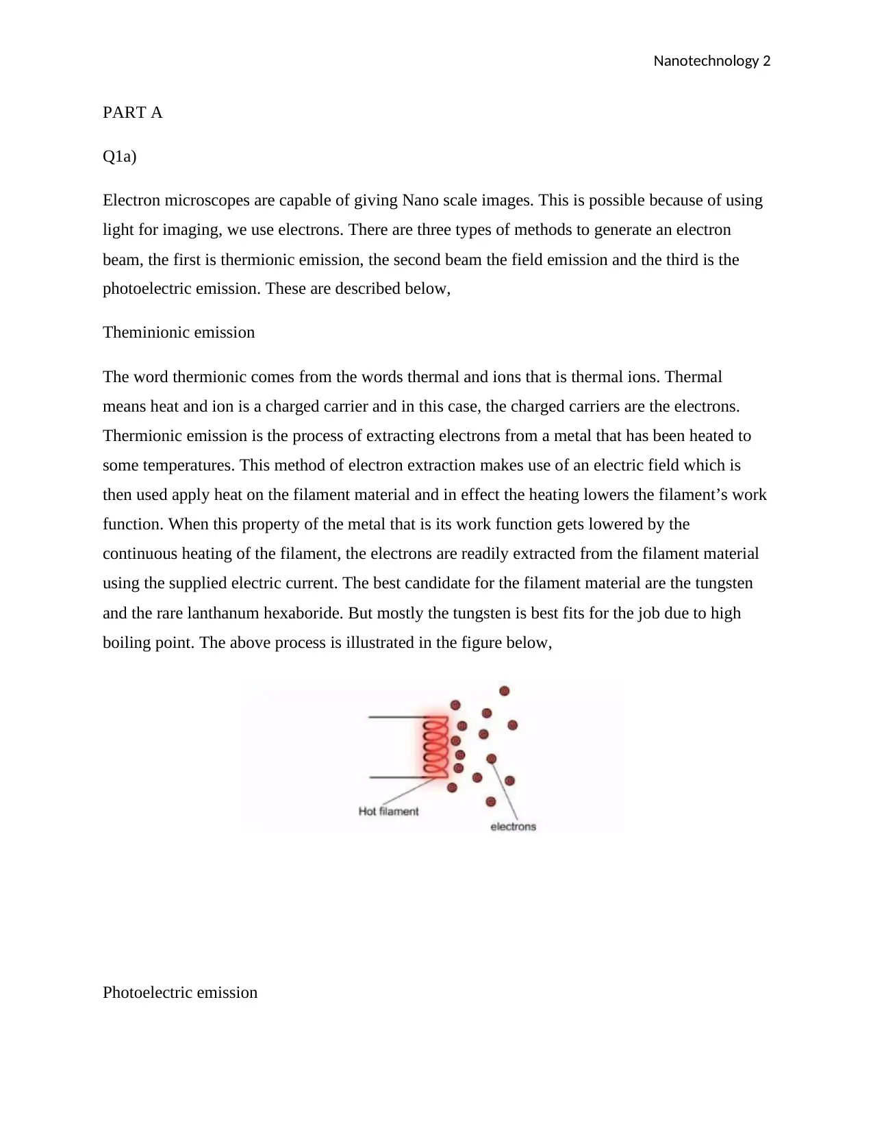
Thermionic emission is the process of extracting electrons from a metal that has been heated to
some temperatures. This method of electron extraction makes use of an electric field which is
then used apply heat on the filament material and in effect the heating lowers the filamentβs work
function. When this property of the metal that is its work function gets lowered by the
continuous heating of the filament, the electrons are readily extracted from the filament material
using the supplied electric current. The best candidate for the filament material are the tungsten
and the rare lanthanum hexaboride. But mostly the tungsten is best fits for the job due to high
boiling point. The above process is illustrated in the figure below,
Photoelectric emission
Nanotechnology 3
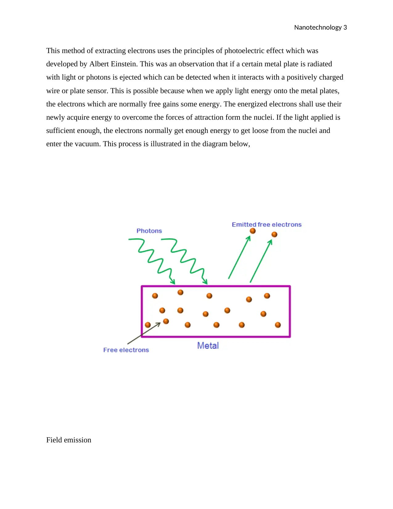
This method of extracting electrons uses the principles of photoelectric effect which was
developed by Albert Einstein. This was an observation that if a certain metal plate is radiated
with light or photons is ejected which can be detected when it interacts with a positively charged
wire or plate sensor. This is possible because when we apply light energy onto the metal plates,
the electrons which are normally free gains some energy. The energized electrons shall use their
newly acquire energy to overcome the forces of attraction form the nuclei. If the light applied is
sufficient enough, the electrons normally get enough energy to get loose from the nuclei and
enter the vacuum. This process is illustrated in the diagram below,
Field emission
Nanotechnology 4
Field emission method of electron emission is a valid demonstration of the quantum mechanical
effects that occur is metal surfaces. This invention was made possible by Erwin Muller in the
1936. The device used for imaging images the crystalline structure of the tungsten needle tip.
The needle tip which usually of a radius of one micron, is in the center of a spherical glass bulb
under high vacuum. With over 10000 volts applied, the electric field is so strong at the needle tip
that electrons are spontaneously emitted to travel along the radial field line and impact on a zinc
sulfide screen of radius 5cm
Q1b
From the Schrodingerβs equations
-h2/2m * d2p(x)/dx2=(E-V) px
but
p(x)=Ae-(β2m(V-E/) h2*x
V represents the particle potential energy. To the left of the barrier, the particle does not
experience any potential energy because nothing is compelling it to move in a certain way so
V=0
The particle has only its energy moving it around E. h is the Planckβs constant. M is the mass.
The probability of finding the particle inside the barrier if the barrier potential energy is greater
than the particles energy that is V>E
Secure Best Marks with AI Grader
Need help grading? Try our AI Grader for instant feedback on your assignments.
Nanotechnology 5
p(x)=e(β2m(pos)/h2) *x
p(x)=e-x (positive #)
This represent the particle decay.
substituting back for Ξ²=(2Ο/h)2m[Uo-E]1/2
We get p(x)=e-2Ξ²
Q1c
(i)
The Richardson equation is used to find show the relationship between current density of a
thermionic emission to the work function(W) and the temperature of the material emitting the
electrons.
js=A T2 exp(-W/kT) β¦β¦β¦β¦β¦β¦β¦. (1)
js=current density of the emission given is (mA/mm2)
A=Richardsonβs constant A=4*nmek2/h^3 which is approximately 1202mA/mm2K2 where m is the
mass and e is elementary charge and his plankβs constant
K is the Boltzman constant given by 8.6173324E-5 eV K-1
making the temperature the subject of the equation (1)
T==js/(A*exp(-W/K)
Nanotechnology 6
but js= 6.1*1010 Am-2
A=5*105 A m-2 K-2
K=8.6173324E-5
therefore, T=js= 6.1*1010 Am-2/ (5*105 *8.6173324E-5)
T=1415751352.471908824 K
Q1c
(ii)
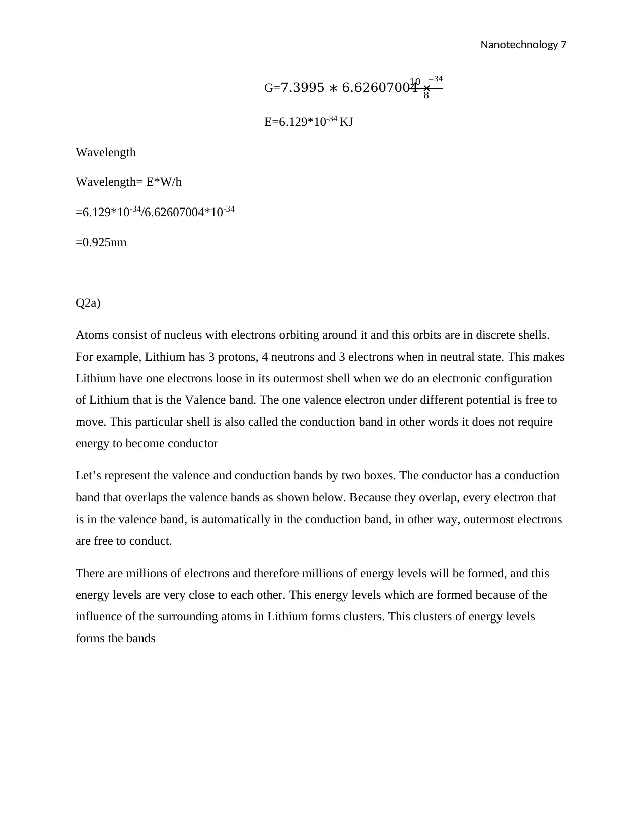
πΊ =2π2
β π
Where G=is the resistivity
N=number of channels
H=plankβs constant
e=energy of particles
making e subject of the formulae
π2 = πΊβ
2π
π =β πΊβ
2π
Substituting we get
Nanotechnology 7
G=7.3995 β 6.62607004 Γ
10 β34
8
E=6.129*10-34 KJ
Wavelength
Wavelength= E*W/h
=6.129*10-34/6.62607004*10-34
=0.925nm
Q2a)
Atoms consist of nucleus with electrons orbiting around it and this orbits are in discrete shells.
For example, Lithium has 3 protons, 4 neutrons and 3 electrons when in neutral state. This makes
Lithium have one electrons loose in its outermost shell when we do an electronic configuration
of Lithium that is the Valence band. The one valence electron under different potential is free to
move. This particular shell is also called the conduction band in other words it does not require
energy to become conductor
Letβs represent the valence and conduction bands by two boxes. The conductor has a conduction
band that overlaps the valence bands as shown below. Because they overlap, every electron that
is in the valence band, is automatically in the conduction band, in other way, outermost electrons
are free to conduct.
There are millions of electrons and therefore millions of energy levels will be formed, and this
energy levels are very close to each other. This energy levels which are formed because of the
influence of the surrounding atoms in Lithium forms clusters. This clusters of energy levels
forms the bands
Paraphrase This Document
Need a fresh take? Get an instant paraphrase of this document with our AI Paraphraser
Nanotechnology 8
Q2b
Density of states
There are many energy levels in a particular band, that we know. Now we want to know how
many are their per unit energy that is what is the distribution of this states within the band and
that is what we mean by density of state
Density of state=No of states per unit energy per unit volume within that particular band
but separation between levels is inversely proportional to the interaction of atoms
Separation between levels β 1/Interaction of atoms
Let g(E)=a function of density state
g(E)d(E) can be defined as the number of states g(E) in the energy interval E E+dE per
unit volume
When we Integrate
ππ£(πΈβ² ) = β« π (πΈ)π(πΈ)
πΈβ²
0
Sv gives the total number of states below Eβ per unit volume.
Consider electron in a 3D potential well.
We know for 3D potential well
πΈ = ( β2
8π2πΏ2 )
L=Size of each side of the cube
N=integers
Because it is a solid, L is much larger than the latex parameter a
Nanotechnology 9
L>> a
Limiting our self to only free electrons in the state, we then we can arrive at the density.
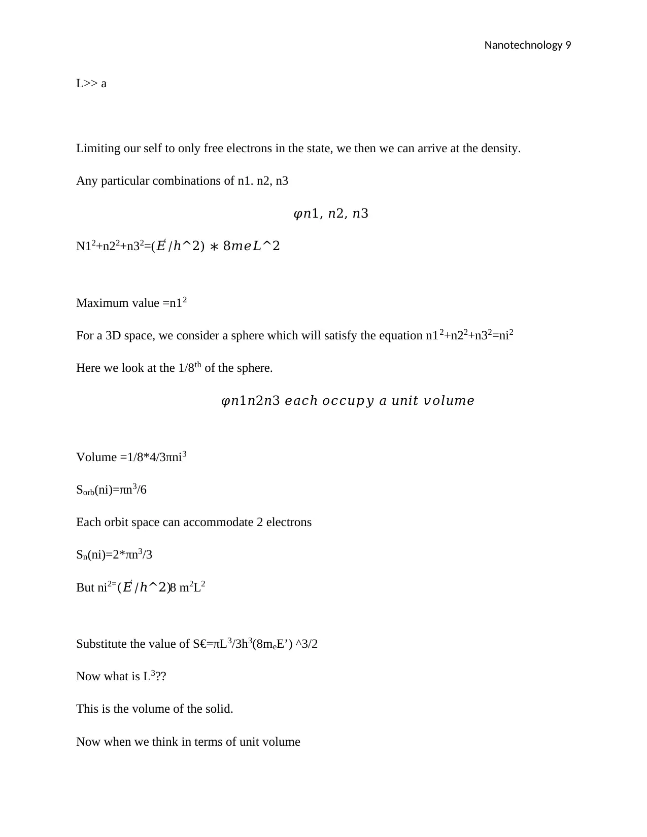
Any particular combinations of n1. n2, n3
ππ1, π2, π3
N12+n22+n32=(πΈβ² /β^2) β 8πππΏ^2
Maximum value =n12
For a 3D space, we consider a sphere which will satisfy the equation n12+n22+n32=ni2
Here we look at the 1/8th of the sphere.
ππ1π2π3 πππβ ππππ’ππ¦ π π’πππ‘ π£πππ’ππ
Volume =1/8*4/3Οni3
Sorb(ni)=Οn3/6
Each orbit space can accommodate 2 electrons
Sn(ni)=2*Οn3/3
But ni2=(πΈβ² /β^2)8 m2L2
Substitute the value of Sβ¬=ΟL3/3h3(8meEβ) ^3/2
Now what is L3??
This is the volume of the solid.
Now when we think in terms of unit volume
Nanotechnology 10
Sv(Eβ)=Ο/3h3(8meEβ)
Number of state per unit volume below Eβ is got by differentiating with respect to g will give us
the density of state.
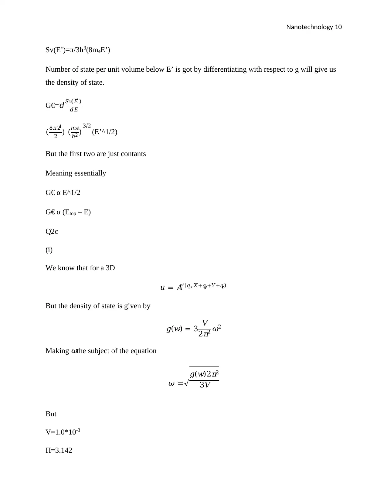
Gβ¬=πππ£(πΈβ² )
ππΈ
(8π21
2 ) (ππ
β2 )3 2β
(Eβ^1/2)
But the first two are just contants
Meaning essentially
G⬠α E^1/2
Gβ¬ Ξ± (Etop β E)
Q2c
(i)
We know that for a 3D
π’ = π΄πβ²(ππ₯π+ππ¦+π+ππ§)
But the density of state is given by
π(π€) = 3 π
2π2 π2
Making πthe subject of the equation
π =β
π(π€)2π2
3π
But
V=1.0*10-3
Ξ =3.142
Secure Best Marks with AI Grader
Need help grading? Try our AI Grader for instant feedback on your assignments.
Nanotechnology 11
g(w) =8920
therefore
Ο=8920β2β3.1422
3β10β3
=5.8706*107 electrons
(ii)
Fermi energy E is given by
πΈ =β2π2
2π
But m is the mass. m is given by the equation
π = π β π£
But k is
π = π32
2
Therefore
πΈ =
β2 β π32
2
2 β π β π
6.62607004 β 10β34 β 3.14223
2
2 β 8920 β 10β3
5.6867 β 10β30π½
iii)
Total energy g(E) is given by the formula
π(πΈ) = 1
2π2
2π
β2
3
2
πΈ
1
2
Nanotechnology 12
But M=π β π
Therefore
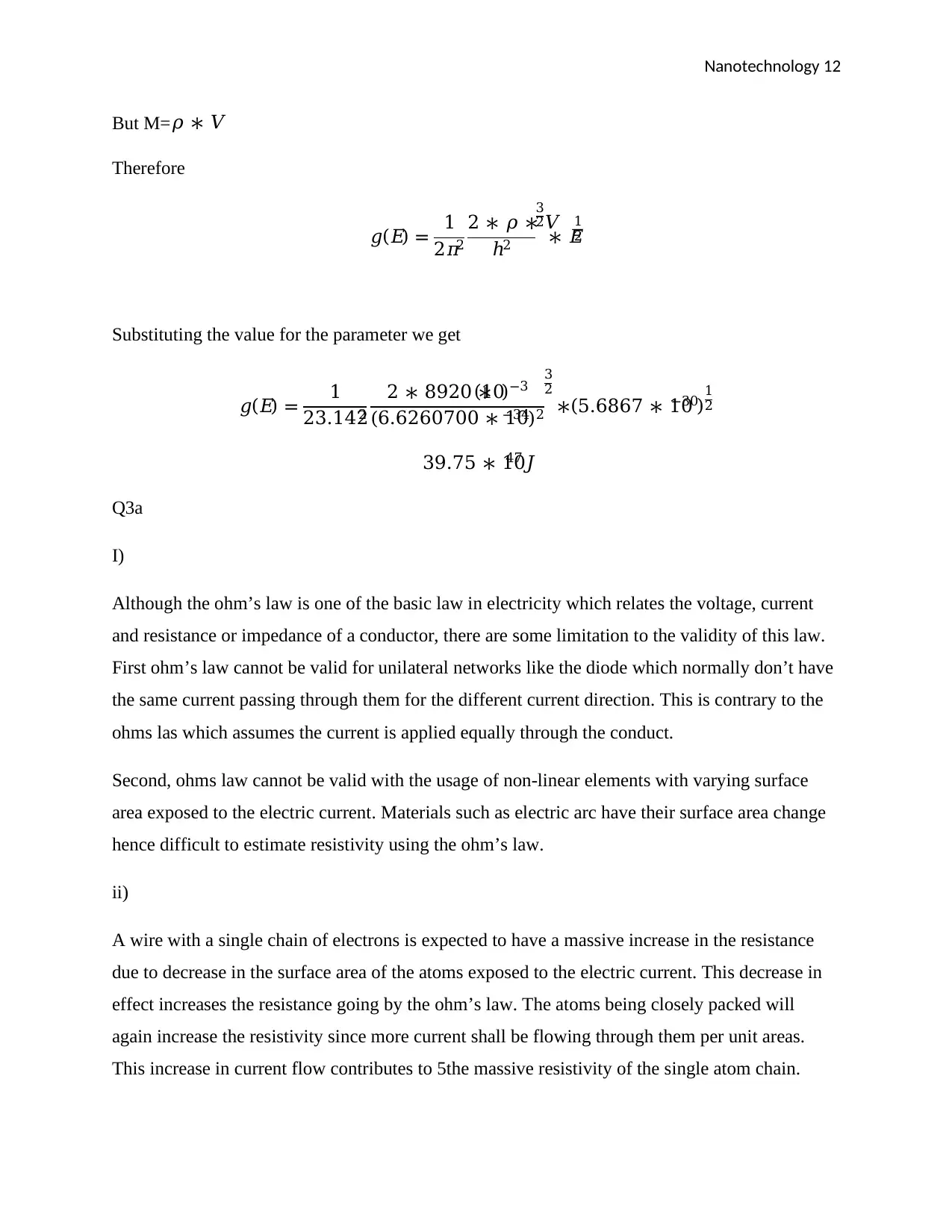
π(πΈ) = 1
2π2
2 β π β π
β2
3
2
β πΈ
1
2
Substituting the value for the parameter we get
π(πΈ) = 1
23.1422
2 β 8920 β(10)β3
(6.6260700 β 10β34)2
3
2
β(5.6867 β 10β30)1
2
39.75 β 1047π½
Q3a
I)
Although the ohmβs law is one of the basic law in electricity which relates the voltage, current
and resistance or impedance of a conductor, there are some limitation to the validity of this law.
First ohmβs law cannot be valid for unilateral networks like the diode which normally donβt have
the same current passing through them for the different current direction. This is contrary to the
ohms las which assumes the current is applied equally through the conduct.
Second, ohms law cannot be valid with the usage of non-linear elements with varying surface
area exposed to the electric current. Materials such as electric arc have their surface area change
hence difficult to estimate resistivity using the ohmβs law.
ii)
A wire with a single chain of electrons is expected to have a massive increase in the resistance
due to decrease in the surface area of the atoms exposed to the electric current. This decrease in
effect increases the resistance going by the ohmβs law. The atoms being closely packed will
again increase the resistivity since more current shall be flowing through them per unit areas.
This increase in current flow contributes to 5the massive resistivity of the single atom chain.
Nanotechnology 13
Q3b
Electron have a function of π(π, π, π) = ππ₯(π) + ππ¦(π) + π(Z)
And the probabilities associated with the instant density given as
π½(π₯, π¦, π§) = ( β
ππ
) 1π(πβπ)
Current passing through the wire is πΌπ₯ =β« β« (βπ)π½(π, π, π). ππ₯ππππ§
π§π¦
πβ ππβ β« β«
β
π§
1π (
π β π
ππ₯ π) ππ¦ππ§β
π¦
πβ
πππ(π¦)2 β¨ 2 β¨ ππ§(π)2 β¨ 1π(ππ₯(π))πππ₯ β(π) ππ¦ππ§ ππ₯β
When we normalize we get
β« β« |π π¦(π)|2
π§π¦
|ππ§(π)|2ππ¦ππ§ = 1
Consequently πβ
ππ 1m(ππ₯(X))πππ₯(π)
ππ₯
But πΊ =2π2π
β
Resistance of the wire is given by π 0 = β
2π2
This is what known as the quantum resistance
Paraphrase This Document
Need a fresh take? Get an instant paraphrase of this document with our AI Paraphraser
Nanotechnology 14
Q3C
i
We Know πΊ =2π2π
β
Where G=quantum resistance
N=number of channels
h=Planckβs constant
e=energy
But we are given
G=7.3995Kilo ohms
making N subject of the formulae
π =πΊβ
2π
=3.69975
Approximately 4 channels
ii)
πΊ =2π2
β π
Where G=is the resistivity
Q3C
i
We Know πΊ =2π2π
β
Where G=quantum resistance
N=number of channels
h=Planckβs constant
e=energy
But we are given
G=7.3995Kilo ohms
making N subject of the formulae
π =πΊβ
2π
=3.69975
Approximately 4 channels
ii)
πΊ =2π2
β π
Where G=is the resistivity
Nanotechnology 15
N=number of channels
H=plankβs constant
e=energy of particles
making e subject of the formulae
π2 = πΊβ
2π
π =β πΊβ
2π
Substituting we get
G=7.3995 β 6.62607004 Γ
10 β
β34
8
E=6.129*10-34 KJ
Wavelength
Wavelength= E*W/h
=6.129*10-34/6.62607004*10-34
=0.925 micrometer
Q4a
i)
Measurements of such quantum dots show that most of the time this system does not conduct,
but there do exist conductance peaks which are fairly regularly spaced. This is referred to as
coulomb blockade. Conduction through this system occurs via sequential tunneling of an
electron from the source to the quantum dot, and then from the quantum dot to the drain.
Nanotechnology 16
However, the addition of the electron to the quantum dot will substantially change the energy of
the dot, in particular, the Coulomb repulsion of the added electron blocks the addition of further
electrons.
ii)
However, the addition of the electron to the quantum dot will substantially change the energy of
the dot, in particular, the Coulomb repulsion of the added electron blocks the addition of further
electrons.
ii)
Secure Best Marks with AI Grader
Need help grading? Try our AI Grader for instant feedback on your assignments.
Nanotechnology 17
b)
The maximum coulomb blockade is given by
|V| = π
2π
The capacitor is presumed to be independent of N and the charging energy which is taken as
U(N)
π(π)
π =
U= π
2πΆ
Thus
| V| = π
2πΆ
Charge on the island is given by the expression
Q = C1(V - V1) + C2(V - V2) + Cg1(V - Vg1) + Cg2(V - Vg2) + C0V.
We can derive the voltage by
V(n) = (-ne + Q0 + C1V1 + C2V2 + Cg1Vg1 + Cg2Vg2)/CΞ£.
Nanotechnology 18
The electrostatic charge required to bring from the ground to up is given by the formulae below
-e
β« V(n)dq = -eV(n) + eΒ²/(2CΞ£).
0
Charge required to remove an electron from up to ground is given by the formulae
e
β« V(n)dq = eV(n) + eΒ²/(2CΞ£).
When we differentiate we get
βE=(e(Q-e/2))/C
C(i)
We know that capacitance is given by the formulae
πΆ =ππ΄
π
Where e is the permissivity and A is the cross-sectional area and d is the diameter width.
Substituting for the values,
e=10
A=1*10-6
d=5*10-5
therefore
C=10β1β10β6
5β10β5
Nanotechnology 19
=2*10-1
But for minimum temperature
KBT<π2
2π
KBT< 102
2β2β10β1
KBT<2.5*103 K
Therefore, minimum temperature shall be 2500K
(ii)
βπΈ =
π2 β π2
2πΆ
βπΈ = πππ₯πππ’ππππ‘πππ πππππππππ¦
π2 = ππππππ π ππ£ππ‘π¦
πΆ = πππππππ‘ππππ
π2 = π‘πππππππ‘π’ππ β ππππ£ππ
Therefore, the maximum potential energy
2.5 β 103 β 10
2 β 2 β 10β1
6.25 β 104π½
Paraphrase This Document
Need a fresh take? Get an instant paraphrase of this document with our AI Paraphraser
Nanotechnology 20
Q5
i.
ii.
Function of parts
Gate
Acts as an electrode
Drain
Acts as an electrode
Source
Acts as an electrode
Q5
i.
ii.
Function of parts
Gate
Acts as an electrode
Drain
Acts as an electrode
Source
Acts as an electrode
Nanotechnology 21
iii.
The island of the single electron transistor, even if very small (nanometric scale) still contains a
very large number of electrons (β 109). Yet, through tunneling, one can add or subtract electrons
from the island charging it either negatively or positively (James, 2010). The extra electrons that
charge the island are called excess electrons and their number is designed by n. The number of
excess electrons can also be negative, meaning that electrons have been removed leaving a
positive charge on the island (one could talk of excess holes in this case). The presence of excess
electrons affects the electrostatic energy of the system, which depends on the charging energy of
the SET:
b)
i.
From
G= Β½
Multiplying both side by 2
β CGV2 =2G
- CGV2C+CG2V2 = 2GGC+CGG
- CGVC+CGV) 2 = 2 GC+CGG
- CGVC+CGV) =β2πΊπΆ + πΆπΊπΊ
- CGVC+CGV) +ne =β2πΊπΆ + πΆπΊπΊ
- CGVC+CGV) =β2πΊπΆ + πΆπΊπΊ+ ne
V(πΆπΊ- CGC+CG) = β2πΊπΆ + πΆπΊπΊ+ne
π(πΆπΊβπΆπΊπΆ+πΆπΊ)
(πΆπΊβπΆπΊπΆ+πΆπΊ) = β2πΊπΆ+πΆπΊπΊ
(πΆπΊβπΆπΊπΆ+πΆπΊ) +ne
V= β2πΆ++ππ
(2πΆπΊβπΆπΊπΆ)
Nanotechnology 22
ii,
The energy needed to raise an electron to a higher energy level in an atom or to remove it from
the same atom. In some cases, it is referred to as resonance potential
c)
From V= β2πΆ++ππ
(2πΆπΊβπΆπΊπΆ)
V= 0.6 b
CG= 1.0Γ10-18
C=0.3 Γ10-18
β2Γ0.3Γ10β18+1.8Γ10β18+ππ
(2Γ10β18β2Γ3Γ10β36) = 0.6
1.2649Γ10β18
2Γ10β18 +ne = 0.6
632455536ne= 0.6
ne= 0.6
632455532
ne= 9.486Γ10-10
iv.
From
G= Β½
G= Β½
G= Β½
G= (β2.998Γ10β19
1.3Γ10β18 ) - 3.88Γ10-19
G = - 0.1115 j (negative indicates that the energy is evolved)
Secure Best Marks with AI Grader
Need help grading? Try our AI Grader for instant feedback on your assignments.
Nanotechnology 23
Q6
a)
I. Diamagnetism
It is a quantum mechanical effect that occurs in all materials; when it is the only contribution to
the magnetism, the material is called diamagnetic. In paramagnetic and ferromagnetic
substances, the weak diamagnetic force is overcome by the attractive force of magnetic dipoles
in the material
II. Paramagnetism
It refers to a property of materials that are weakly attracted to a magnetic field.
III. Ferromagnetism
This is a physical phenomenon in which certain electrically uncharged materials strongly attract
others.
B (i)
In magnetic materials, dipole is always aligned in a particular direction to achieve magnetism.
Nut not all the dipoles are aligned, this because the dipoles are always in motion by virtue of
being atoms. This motion is possible due to thermal energy. So due to thermal energy, they are
always in motion
If we lower the temperature, energy becomes less. This I effect increase the magnetism since
there will be les random motion hence more will align
Therefore π =πΆπ΅0
π
Where M=magnetism
Nanotechnology 24
T=temperature and C=Curie constant
6
Bii)
From the expression below, Susceptibility is π = πΆ
πβππ
The induced magnetism can be expressed π = ππ
The magnitude force of the magnetization can be derived from
π = πππ΅0
1 β πππΎ
But we know from the Curie law ππ = πΆ
π where C denotes the Curie constant.
Susceptibility can therefore be found
π =π
π΅0
= πΆ
π β πΆπΎ
= πΆ
π β ππ
We can now find the Curie Temperature Tc from the following the Curie law,
ππ = ππΎπ2π2π΅
3ππ΅
According to the Curie law,
ππΌπΆ
Replacing C by the field exchanged,
π΅πΈ = πΎπ
Nanotechnology 25
π = πππ½ππ΅π΅π½(ππ½ππ΅πΎπ
ππ )
To reduce the above equation π = πππ½ππ΅π
And use it to reduce temperature π‘ = πΎπ
ππ2π2π½2πΎ
Whence
M=ππ΅
c)
Magnetic moment= π
ππ½
But J=2
But h= π
π
Magnetic moment = h*J
But h is the Planckβs constant
h= 6.62607004 Γ 10-34
therefore, moment=6.62607004 Γ 10-34 *2
=1.3252*10^-33 kgm^2s^-2
PART B
Q 2
a)
i.
The electron beam produces X-ray photons in the interaction of beam-specimen volume
underneath the surface of specimen. Several X-ray photons coming from the specimen contains
energies basically to the specimen elements; these are the characteristic X-rays which gives the
Paraphrase This Document
Need a fresh take? Get an instant paraphrase of this document with our AI Paraphraser
Nanotechnology 26
SEMβs logical abilities. (Daniels, 2012). Beam electrons can undertake negative acceleration in
the Coulombian field of the specimen atoms that relates to a loss in energy in electron. This can
be illustrated by the following diagram;
There is interact of beam electron with firmly bound inner energy level electrons of a specimen
atom, disgorging an electron from an energy level. The atom will hence be left in an energetic
and excited state.
ii.
Generated by interactions which is purely inelastic having a high energy electron with valence
electrons in the specimen atoms, resulting to the ejection of the electrons from the specimen
atoms. These ejected valence electrons are known as the secondary electrons.
Nanotechnology 27
This will result to a slight loss in energy and change in path in the incident electron. Every
incident electron can generate several secondary electrons.
b)
En=E1 1
π2
But E1 = πππ4
32π2π0π2
Applying this to inner electron of a large atom will hence be as below
En= πππ4
32π2π0π2 ( 1
π2) β¦β¦β¦β¦β¦β¦β¦β¦β¦β¦β¦β¦β¦β¦β¦β¦β¦β¦β¦β¦β¦β¦β¦β¦β¦β¦β¦β¦ i
En can also be given in the following ways
En= hv , C= vπ and V Μ = 1
π
Hence;
V Μ = πΈπ
βπΆ
V Μ = 1
π= πππ4
32π2π0π2 ( 1
π2)
For inner electron of a large atom
En=βE=En2=En1
Nanotechnology 28
Therefore;
En= (2π2π2ππ§2π2
β2 ) ( 1
π12 β 1
π22)
And from the Rydberg constant R
R= (2π2π2ππ2
πΆβ3 )
V= RZ2 ( 1
π12 β 1
π22)= 1
π
RZ-1 πππ2
24π2π0π2
V= = 1
π
V= R(Z-1)2 0.75 =1
π
1
π= R(Z-1)2 3
4
C)
Z=28
R=1.097Γ107
Therefore;
En= (2π2π2ππ§2π2
β2 ) ( 1
π12 β 1
π22)
And from the Rydberg constant R
R= (2π2π2ππ2
πΆβ3 )
V= RZ2 ( 1
π12 β 1
π22)= 1
π
RZ-1 πππ2
24π2π0π2
V= = 1
π
V= R(Z-1)2 0.75 =1
π
1
π= R(Z-1)2 3
4
C)
Z=28
R=1.097Γ107
Secure Best Marks with AI Grader
Need help grading? Try our AI Grader for instant feedback on your assignments.
Nanotechnology 29
And from f = ππ(π)
4ππ0π 2
F= 28Γ1.6Γ10β19
4Γ3,142Γ8.854Γ10β12
F= 4.0259Γ108 Hz
Q 3
a)
Quantum resistance refers to cryptographic algorithms which is always a public key algorithm
which believed to be more secure against any attack that are thought to be secure against an
attack by a quantum computer.
Conditions
When there are narrower incompressible strips
During the hall condition.
Limitations
Here, it drives in chemically synthesized semiconductor nanowires as Nano electronic gadgets.
We to begin with current important nanowire field-effect transistor structures and survey comes
about gotten from both p- and n-channel homogeneous composition nanowires. Moment, we
portray nanowire heterostructures, appear that by utilizing nanowire heterostructures, a few
Nanotechnology 30
restricting variables in homogeneous nanowire gadgets can be moderated, and illustrate that
nanowire transistor execution can reach the ballistic restrain and surpass state-of-the-art. Third,
we examine essential strategies for organization of nanowires essential for creating clusters of
gadget and circuits. Fourth, we present the concept of crossbar nanowire circuits, talk about
comes about for both transistor and nonvolatile switch gadgets, and depict special approaches for
multiplexing/multiplexing empowered by artificially coded nanowire.
b)
β΄(V) = 1
βππ
In a 1 D the voltage is shown as
V= π1βπ2
π
And
ππ
ππ= 2
βπ£, where e is the electron charge And the density state of 1 D state is given by
β΄(V) = 1
βππ
Where h is the Planck constant and v is the velocity
β΄(V) = 1
βππ= -ev (V1-V2 ) ππ
ππ
1
βππ= -ev ππ
ππ
1
βππ
= - e2v = 2
βπ£RQ
h= (-2e)2 RQ
h= 4e2 RQ
RQ= β
4π2
C)
i. The total number of channel in conduction process
Nanotechnology 31
0.4+ 1 = 1.4
Therefore
0.4Γ1.897Γ1000
π = 172 channels
1Γ1.897Γ1000
π = 431 channels
Total channels = 431 + 172
Total channels = 603 channels
ii.
Energy
Energy = R(1+Ξ±d)
Energy = 1897(1 + 0.4Γ10-9)
E= 1897Γ1.000002
E= 1897.000002 joules
Wavelength
β
π=πΈ
πΆ
6.6260Γ10β34
π = 1897
3Γ108
π= 1.0478Γ10-28 m
Q4
Paraphrase This Document
Need a fresh take? Get an instant paraphrase of this document with our AI Paraphraser
Nanotechnology 32
a)
i)
Measurements of such quantum dots show that most of the time this system does not conduct,
but there do exist conductance peaks which are fairly regularly spaced. This is referred to as
coulomb blockade. Conduction through this system occurs via sequential tunneling of an
electron from the source to the quantum dot, and then from the quantum dot to the drain.
However, the addition of the electron to the quantum dot will substantially change the energy of
the dot, in particular, the Coulomb repulsion of the added electron blocks the addition of further
electrons.
ii)
Nanotechnology 33
b)
The maximum coulomb blockade is given by
|V| = π
2π
The capacitor is presumed to be independent of N and the charging energy which is taken as
U(N)
π(π)
π =
U= π
2πΆ
Thus
| V| = π
2πΆ
b)
The maximum coulomb blockade is given by
|V| = π
2π
The capacitor is presumed to be independent of N and the charging energy which is taken as
U(N)
π(π)
π =
U= π
2πΆ
Thus
| V| = π
2πΆ
Nanotechnology 34
c)
i.
Thickness = 0.5
Junction area = 1Γ1 nm2
πT= 10
From E = Β½ CV2
And C =
ππ΄
π β¦β¦β¦β¦β¦β¦β¦β¦β¦β¦β¦β¦β¦β¦β¦β¦β¦β¦β¦β¦β¦β¦β¦β¦β¦β¦β¦β¦β¦β¦β¦β¦β¦β¦β¦ i
And the capacitance temperature coefficient is taken as 850C
πΆπβπΆπ
πΆπΓ(πβ25) Γ 10 -6 = CTC β¦β¦β¦β¦β¦β¦β¦β¦β¦β¦β¦β¦β¦β¦β¦β¦β¦β¦β¦β¦β¦β¦β¦β¦β¦. ii
And from equation i above
C= 10Γ1Γ10β18
0.5Γ10β9
C= 20nF
From equation ii above
20βπΆπ
πΆπΓ(πβ25) Γ 10 -6 = 85
20000000 β Tmin = 5101Tmin
Tmin = 20000000
5101
Secure Best Marks with AI Grader
Need help grading? Try our AI Grader for instant feedback on your assignments.
Nanotechnology 35
Tmin = 19.890C
ii.
The potential required at lower temperature can be obtained as below, and a lower temperature
can be taken as 100C
And E = 3
2 kT
K= 1.38Γ 10 -13 j/k
T =10 (283 K)
E= Β½Γ20Γ10-19 ΓV2= 5.851Γ10-11
V2 = 5.8581Γ10β11
1Γ10β3
V= 0.0765 Volts
5
a)
i)
Tmin = 19.890C
ii.
The potential required at lower temperature can be obtained as below, and a lower temperature
can be taken as 100C
And E = 3
2 kT
K= 1.38Γ 10 -13 j/k
T =10 (283 K)
E= Β½Γ20Γ10-19 ΓV2= 5.851Γ10-11
V2 = 5.8581Γ10β11
1Γ10β3
V= 0.0765 Volts
5
a)
i)
Nanotechnology 36
Pico slider
The function of the pico slider is to give a physical support to the head and keep it in the desired
position which is relative to the platter as the head floats over its surface.
Inductive write GMR reader sensor
Its function is to move above the disk platter and transform the platter's magnetic field into
electrical current (read the disk) or, vice versa, transform electrical current into magnetic field
(write the disk).
Copper write coil
The function of the copper write coil is to aid in conduction of electrical energy.
Antiferromagnetic exchange film
Nanotechnology 37
It was shown that 6 nm of IrMn is a critical thickness for the exchange bias appearance.
Therefore, Antiferromagnetic exchange film provides a suitable thickness for the operation.
Inductive write head
It is used to senses (reads) and records (writes) info on a tape or magnetic disk. For recording,
the surface of the disk or tape is moved past the head of read/write.
ii).
The resistance of metals relies on the pitiless free way of their conduction electrons, which, in
GMR contraptions, depends on the turn presentation. In ferromagnetic materials, conduction
electrons either turn up when their turn is parallel to the alluring diminutive of the ferromagnet,
or turn down when they are antiparallel (Daniels, 2012). In nonmagnetic conductors, there are
rise to numbers of spin-up and spin-down electrons in all imperativeness bunches. Since of the
ferromagnetic exchange interaction, there's a refinement between the number of spin-up and
spin-down electrons inside the conduction bunches. Quantum mechanics coordinates that the
probability of an electron being scattered when it passes into a ferromagnetic conductor depends
on the heading of its turn. In common, electrons with a turn adjusted with the bigger portion of
turns inside the ferferromagnets will travel assist without being scattered (James, 2010).
approaches for multiplexing/demultiplexing empowered by artificially coded nanowire.
iii)
Paraphrase This Document
Need a fresh take? Get an instant paraphrase of this document with our AI Paraphraser
Nanotechnology 38
b)
For a single phase proximity;
Fb= 4 [πΊππ
πΊππ·
]2 [π π
π 0β 1]
Where; fb is the factor which is accountable for proximity effect, GMR is geometric mean radius
of the same conductor, GMD is the mean spacing between the conductors, RH is total resistance
at aligned and R0 is total resistance at antiparallel.
π π»
π 0- 1 + 1 = ππ
4[πΊππ
πΊππ·
] +1
RH= )
RH= )
c)
βR= RH-R0
Nanotechnology 39
βR = -20 Ξ©
Down channel is 10 Ξ©
Up channel will hence be a negative
-20= 10 - - Rup
-20= 10+Rup
Rup = -20-10
Rup = -30 Ξ©
6
a)
IV. Diamagnetism
It is a quantum mechanical effect that occurs in all materials; when it is the only contribution to
the magnetism, the material is called diamagnetic. In paramagnetic and ferromagnetic
substances, the weak diamagnetic force is overcome by the attractive force of magnetic dipoles
in the material
V. Paramagnetism
It refers to a property of materials that are weakly attracted to a magnetic field.
VI. Ferromagnetism
Nanotechnology 40
This is a physical phenomenon in which certain electrically uncharged materials strongly attract
others.
b)
From Maxwell- Boltzman distribution
πππππΘ
πππ€ππΘ = exp(βπΈπ’ππππβπΈπππ€ππ
ππ ) = exp (ββπΈ
ππ ) = exp (βπ
ππ
) = exp (ββπ
ππ ) β¦β¦β¦β¦β¦β¦β¦. EPR
equation
And the sensitivity of the EPR depends on photon frequency v according to the below equation
Nmin = πΎ1π
π0πππ£2πΒ½
K1 is a constant, v is a sample volume Q0 is unloaded quality factor, kf is the cavity filing factor,
p is the microwave power,
The g factor provides more info about a parametric center electronic structure. An unpaired
electron responds not just to a spectrometer but also to any local magnetic field. Effective field
Beff is thus written as
hv= B0( 1- π )
hv= geB0Beffme = geΞΌBeffB0 ( 1- π ) Therefore
hv= geB0Beffme [-g( π
2ππ) ] S
c)
i.
Secure Best Marks with AI Grader
Need help grading? Try our AI Grader for instant feedback on your assignments.
Nanotechnology 41
hv= 75meters
g= 5.585
5.585Γπ΅Γ5.585Γ1.6Γ10β19
2Γ9.1Γ10β31 =75
B= 2.735 Γ10-11
ii.
From orbital
ΞΌL= -gL π
2ππ L
ΞΌLz = -gL π
2ππ ml = -ml ΞΌ g ( since gL = 1 )
ΞΌs= -gs π
2ππ S , ΞΌSz =- gs πβ
2ππ ms
and
ΞΌN= πβ
2ππ and for magnetic moment of neutron ΞΌn = -1.913 ΞΌN
The z component in CODATA value of ΞΌp = -1.45844
The magnetic moment of nucleus of magneton is given as
ΞΌ= πΞΌ ββ
ΞΌz= -1.458444Γ -1.913ΞΌN
ΞΌz= 2.7899957 ΞΌN
ΞΌz= 2.79 ΞΌN
Nanotechnology 42
PART C
Q1a)
Electron microscopes are capable of giving Nano scale images. This is possible because of using
light for imaging, we use electrons. There are three types of methods to generate an electron
beam, the first is thermionic emission, the second beam the field emission and the third is the
photoelectric emission. These are described below,
Theminionic emission
The word thermionic comes from the words thermal and ions that is thermal ions. Thermal
means heat and ion is a charged carrier and in this case, the charged carriers are the electrons.
Thermionic emission is the process of extracting electrons from a metal that has been heated to
some temperatures. This method of electron extraction makes use of an electric field which is
then used apply heat on the filament material and in effect the heating lowers the filamentβs work
function. When this property of the metal that bis its work function gets lowered by the
continuous heating of the filament, the electrons are readily extracted from the filament material
using the supplied electric current. The best candidate for their filament material are the tungsten
and the rare lanthanum hexaboride. But mostly the tungsten is best fits for the job due to high
boiling point. The above process is illustrated in the figure below,
Nanotechnology 43
Photoelectric emission
This method of extracting electrons uses the principles of photoelectric effect which was
developed by Albert Einstein. This was an observation that if a certain metal plate is radiated
with light or photons is ejected which can be detected when it interacts with a positively charged
wire or plate sensor. This is possible because when we apply light energy onto the metal plates,
the electrons which are normally free gains some energy. The energized electrons shall use their
newly acquire energy to overcome the forces of attraction form the nuclei. If the light applied is
sufficient enough, the electrons normally get enough energy to get loose from the nuclei and
enter the vacuum. This process is illustrated in the diagram below,
Paraphrase This Document
Need a fresh take? Get an instant paraphrase of this document with our AI Paraphraser
Nanotechnology 44
Field emission
Field emission method of electron emission is a valid demonstration of the quantum mechanical
effects that occur is metal surfaces. This invention was made possible by Erwin Muller in the
1936. The device used for imaging images the crystalline structure of the tungsten needle tip.
The needle tip which usually of a radius of one micron, is in the center of a spherical glass bulb
under high vacuum. With over 10000 volts applied, the electric field is so strong at the needle tip
that electrons are spontaneously emitted to travel along the radial field line and impact on a zinc
sulfide screen of radius 5cm
Q1b
From the Schrodingerβs equations
-h2/2m * d2p(x)/dx2=(E-V) px
but
p(x)=Ae-(β2m(V-E/) h2*x
V represents the particle potential energy. To the left of the barrier, the particle does not
experience any potential energy because nothing is compelling it to move in a certain way so
V=0
The particle has only its energy moving it around E. h is the Planckβs constant. M is the mass.
Nanotechnology 45
The probability of finding the particle inside the barrier if the barrier potential energy is greater
than the particles energy that is V>E
p(x)=e(β2m(pos)/h2) *x
p(x)=e-x (positive #)
This represent the particle decay.
substituting back for Ξ²=(2Ο/h)2m[Uo-E]1/2
We get p(x)=e-2Ξ²
Q6c
(i)
The Richardson equation is used to find show the relationship between current density of a
thermionic emission to the work function(W) and the temperature of the material emitting the
electrons.
js=A T2 exp(-W/kT) β¦β¦β¦β¦β¦β¦β¦. (1)
js=current density of the emission given is (mA/mm2)
A=Richardsonβs constant A=4*nmek2/h^3 which is approximately 1202mA/mm2K2 where m is the
mass and e is elementary charge and his plankβs constant
K is the Boltzman constant given by 8.6173324E-5 eV K-1
making the temperature the subject of the equation (1)
Nanotechnology 46
T==js/(A*exp(-W/K)
but js= 6.1*1010 Am-2
A=5*105 A m-2 K-2
K=8.6173324E-5
therefore, T=js= 6.1*1010 Am-2/ (5*105 *8.6173324E-5)
T=1415751352.471908824 K
Q6c
(ii)
πΊ =2π2
β π
Where G=is the resistivity
N=number of channels
H=plankβs constant
e=energy of particles
making e subject of the formulae
π2 = πΊβ
2π
π =β πΊβ
2π
Secure Best Marks with AI Grader
Need help grading? Try our AI Grader for instant feedback on your assignments.
Nanotechnology 47
Substituting we get
G=7.3995 β 6.62607004 Γ
10 β34
8
E=6.129*10-34 KJ
Wavelength
Wavelength= E*W/h
=6.129*10-34/6.62607004*10-34
=0.925nm
Q2
Although the ohmβs law is one of the basic law in electricity which relates the voltage, current
and resistance or impedance of a conductor, there are some limitation to the validity of this law.
First ohmβs law cannot be valid for unilateral networks like the diode which normally donβt have
the same current passing through them for the different current direction. This is contrary to the
ohms las which assumes the current is applied equally through the conduct.
Second, ohms law cannot be valid with the usage of non-linear elements with varying surface
area exposed to the electric current. Materials such as electric arc have their surface area change
hence difficult to estimate resistivity using the ohmβs law.
ii)
A wire with a single chain of electrons is expected to have a massive increase in the resistance
due to decrease in the surface area of the atoms exposed to the electric current. This decrease in
effect increases the resistance going by the ohmβs law. The atoms being closely packed will
again increase the resistivity since more current shall be flowing through them per unit areas.
This increase in current flow contributes to 5the massive resistivity of the single atom chain.
Q2b
Electron have a function of π(π, π, π) = ππ₯(π) + ππ¦(π) + π(Z)
Nanotechnology 48
And the probabilities associated with the instant density given as
π½(π₯, π¦, π§) = ( β
ππ
) 1π(πβπ)
Current passing through the wire is
πβ ππβ β« β«
β
π§
1π (
π β π
ππ₯ π) ππ¦ππ§β
π¦
πβ
πππ(π¦)2 β¨ 2 β¨ ππ§(π)2 β¨ 1π(ππ₯(π))πππ₯ β(π) ππ¦ππ§ ππ₯β
When we normalize we get
β« β« |π π¦(π)|2
π§π¦
|ππ§(π)|2ππ¦ππ§ = 1
Consequently πβ
ππ 1m(ππ₯(X))πππ₯(π)
ππ₯
But πΊ =2π2π
β
Resistance of the wire is given by π 0 = β
2π2
This is what known as the quantum resistance
Nanotechnology 49
Q2
ci
We Know πΊ =2π2π
β
Where G=quantum resistance
N=number of channels
h=Planckβs constant
e=energy
But we are given
G=7.3995Kilo ohms
making N subject of the formulae
π =πΊβ
2π
=3.69975
Approximately 4 channels
ii)
Q2
ci
We Know πΊ =2π2π
β
Where G=quantum resistance
N=number of channels
h=Planckβs constant
e=energy
But we are given
G=7.3995Kilo ohms
making N subject of the formulae
π =πΊβ
2π
=3.69975
Approximately 4 channels
ii)
Paraphrase This Document
Need a fresh take? Get an instant paraphrase of this document with our AI Paraphraser
Nanotechnology 50
πΊ =2π2
β π
Where G=is the resistivity
N=number of channels
H=plankβs constant
e=energy of particles
making e subject of the formulae
π2 = πΊβ
2π
π =β πΊβ
2π
Substituting we get
G=7.3995 β 6.62607004 Γ
10 β
β34
8
E=6.129*10-34 KJ
Wavelength
Wavelength= E*W/h
=6.129*10-34/6.62607004*10-34
=0.925nm
Q 4
v.
Nanotechnology 51
i.
ii.
Function of parts
Gate
Acts as an electrode
Drain
Acts as an electrode
Source
Acts as an electrode
iii.
The island of the single electron transistor, even if very small (nanometric scale) still contains a
very large number of electrons (β 109). Yet, through tunneling, one can add or subtract electrons
Nanotechnology 52
from the island charging it either negatively or positively (James, 2010). The extra electrons that
charge the island are called excess electrons and their number is designed by n. The number of
excess electrons can also be negative, meaning that electrons have been removed leaving a
positive charge on the island (one could talk of excess holes in this case). The presence of excess
electrons affects the electrostatic energy of the system, which depends on the charging energy of
the SET:
b)
i.
From
G= Β½
Multiplying both side by 2
β CGV2 =2G
- CGV2C+CG2V2 = 2GGC+CGG
- CGVC+CGV) 2 = 2 GC+CGG
- CGVC+CGV) =β2πΊπΆ + πΆπΊπΊ
- CGVC+CGV) +ne =β2πΊπΆ + πΆπΊπΊ
- CGVC+CGV) =β2πΊπΆ + πΆπΊπΊ+ ne
V(πΆπΊ- CGC+CG) = β2πΊπΆ + πΆπΊπΊ+ne
π(πΆπΊβπΆπΊπΆ+πΆπΊ)
(πΆπΊβπΆπΊπΆ+πΆπΊ) = β2πΊπΆ+πΆπΊπΊ
(πΆπΊβπΆπΊπΆ+πΆπΊ) +ne
V= β2πΆ++ππ
(2πΆπΊβπΆπΊπΆ)
ii,
Secure Best Marks with AI Grader
Need help grading? Try our AI Grader for instant feedback on your assignments.
Nanotechnology 53
The energy needed to raise an electron to a higher energy level in an atom or to remove it from
the same atom. In some cases, it is referred to as resonance potential
c)
From V= β2πΆ++ππ
(2πΆπΊβπΆπΊπΆ)
V= 0.6 b
CG= 1.0Γ10-18
C=0.3 Γ10-18
β2Γ0.3Γ10β18+1.8Γ10β18+ππ
(2Γ10β18β2Γ3Γ10β36) = 0.6
1.2649Γ10β18
2Γ10β18 +ne = 0.6
632455536ne= 0.6
ne= 0.6
632455532
ne= 9.486Γ10-10
iv.
From
G= Β½
G= Β½
G= Β½
G= (β2.998Γ10β19
1.3Γ10β18 ) - 3.88Γ10-19
G = - 0.1115 j (negative indicates that the energy is evolved)
Q5
i)
Nanotechnology 54
Pico slider
The function of the pico slider is to physically support the head and hold it in the correct position
relative to the platter as the head floats over its surface.
Inductive write GMR reader sensor
Its function is to move above the disk platter and transform the platter's magnetic field into
electrical current (read the disk) or, vice versa, transform electrical current into magnetic field
(write the disk).
Copper write coil
The function of the copper write coil is to aid in conduction of electrical energy.
Antiferromagnetic exchange film
Nanotechnology 55
It was shown that 6 nm of IrMn is a critical thickness for the exchange bias appearance.
Therefore, Antiferromagnetic exchange film provides a suitable thickness for the operation.
Inductive write head
It is used to reads (senses) and writes (records) data on a magnetic disk or tape. For writing, the
surface of the disk or tape is moved past the read/write head.
ii).
The resistance of metals depends on the mean free path of their conduction electrons, which, in
GMR devices, depends on the spin orientation. In ferromagnetic materials, conduction electrons
either spin up when their spin is parallel to the magnetic moment of the ferromagnetic, or spin
down when they are antiparallel. In nonmagnetic conductors, there are equal numbers of spin-up
and spin-down electrons in all energy bands. Because of the ferromagnetic exchange interaction,
there is a difference between the number of spin-up and spin-down electrons in the conduction
bands. Quantum mechanics dictates that the probability of an electron being scattered when it
passes into a ferromagnetic conductor depends on the direction of its spin. In general, electrons
with a spin aligned with the majority of spins in the ferromagnets will travel further without
being scattered.
iii)
Paraphrase This Document
Need a fresh take? Get an instant paraphrase of this document with our AI Paraphraser
Nanotechnology 56
b)
For a single phase proximity;
Fb= 4 [πΊππ
πΊππ·
]2 [π π
π 0β 1]
Where; fb is the factor which is accountable for proximity effect, GMR is geometric mean radius
of the same conductor, GMD is the mean spacing between the conductors, RH is total resistance
at aligned and R0 is total resistance at antiparallel.
π π»
π 0- 1 + 1 = ππ
4[πΊππ
πΊππ·
] +1
RH= )
RH= )
c)
βR= RH-R0
Nanotechnology 57
βR = -20 Ξ©
Down channel is 10 Ξ©
Up channel will hence be a negative
-20= 10 - - Rup
-20= 10+Rup
Rup = -20-10
Rup = -30 Ξ©
Q6
6
a)
I. Diamagnetism
It is a quantum mechanical effect that occurs in all materials; when it is the only contribution to
the magnetism, the material is called diamagnetic. In paramagnetic and ferromagnetic
substances, the weak diamagnetic force is overcome by the attractive force of magnetic dipoles
in the material
II. Paramagnetism
It refers to a property of materials that are weakly attracted to a magnetic field.
III. Ferromagnetism
This is a physical phenomenon in which certain electrically uncharged materials strongly attract
others.
B (i)
In magnetic materials, dipole is always aligned in a particular direction to achieve magnetism.
Nut not all the dipoles are aligned, this because the dipoles are always in motion by virtue of
Nanotechnology 58
being atoms. This motion is possible due to thermal energy. So due to thermal energy, they are
always in motion
If we lower the temperature, energy becomes less. This I effect increase the magnetism since
there will be les random motion hence more will align
Therefore π =πΆπ΅0
π
Where M=magnetism
T=temperature and C=Curie constant
6
Bii)
From the expression below, Susceptibility is π = πΆ
πβππ
The induced magnetism can be expressed π = ππ
The magnitude force of the magnetization can be derived from
π = πππ΅0
1 β πππΎ
But we know from the Curie law ππ = πΆ
π where C denotes the Curie constant.
Susceptibility can therefore be found
π =π
π΅0
= πΆ
π β πΆπΎ
= πΆ
π β ππ
We can now find the Curie Temperature Tc from the following the Curie law,
Secure Best Marks with AI Grader
Need help grading? Try our AI Grader for instant feedback on your assignments.
Nanotechnology 59
ππ = ππΎπ2π2π΅
3ππ΅
According to the Curie law,
ππΌπΆ
Replacing C by the field exchanged,
π΅πΈ = πΎπ
π = πππ½ππ΅π΅π½(ππ½ππ΅πΎπ
ππ )
To reduce the above equation π = πππ½ππ΅π
And use it to reduce temperature π‘ = πΎπ
ππ2π2π½2πΎ
Whence
M=ππ΅
c)
Magnetic moment= π
ππ½
But J=2
But h= π
π
Magnetic moment = h*J
But h is the Planckβs constant
h= 6.62607004 Γ 10-34
Nanotechnology 60
therefore, moment=6.62607004 Γ 10-34 *2
=1.3252*10^-33 kgm^2s^-2
Bibliography
Daniels, j., 2012. Physical electronics and nano technology :Generation of electrons. 2nd ed.
Hull: IEEE.
James, F., 2010. coulomb blockade in nanotechnology. 3th ed. manchester : CRC.
therefore, moment=6.62607004 Γ 10-34 *2
=1.3252*10^-33 kgm^2s^-2
Bibliography
Daniels, j., 2012. Physical electronics and nano technology :Generation of electrons. 2nd ed.
Hull: IEEE.
James, F., 2010. coulomb blockade in nanotechnology. 3th ed. manchester : CRC.
1 out of 60
Your All-in-One AI-Powered Toolkit for Academic Success.
Β +13062052269
info@desklib.com
Available 24*7 on WhatsApp / Email
Unlock your academic potential
Β© 2024 Β | Β Zucol Services PVT LTD Β | Β All rights reserved.