MIS Diode Application: Electrical Charging in Flash Memory
VerifiedAdded on 2023/04/21
|4
|1506
|228
Report
AI Summary
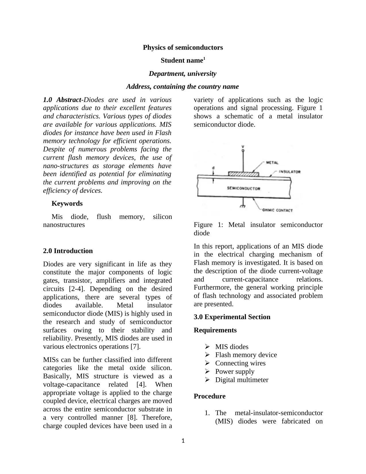
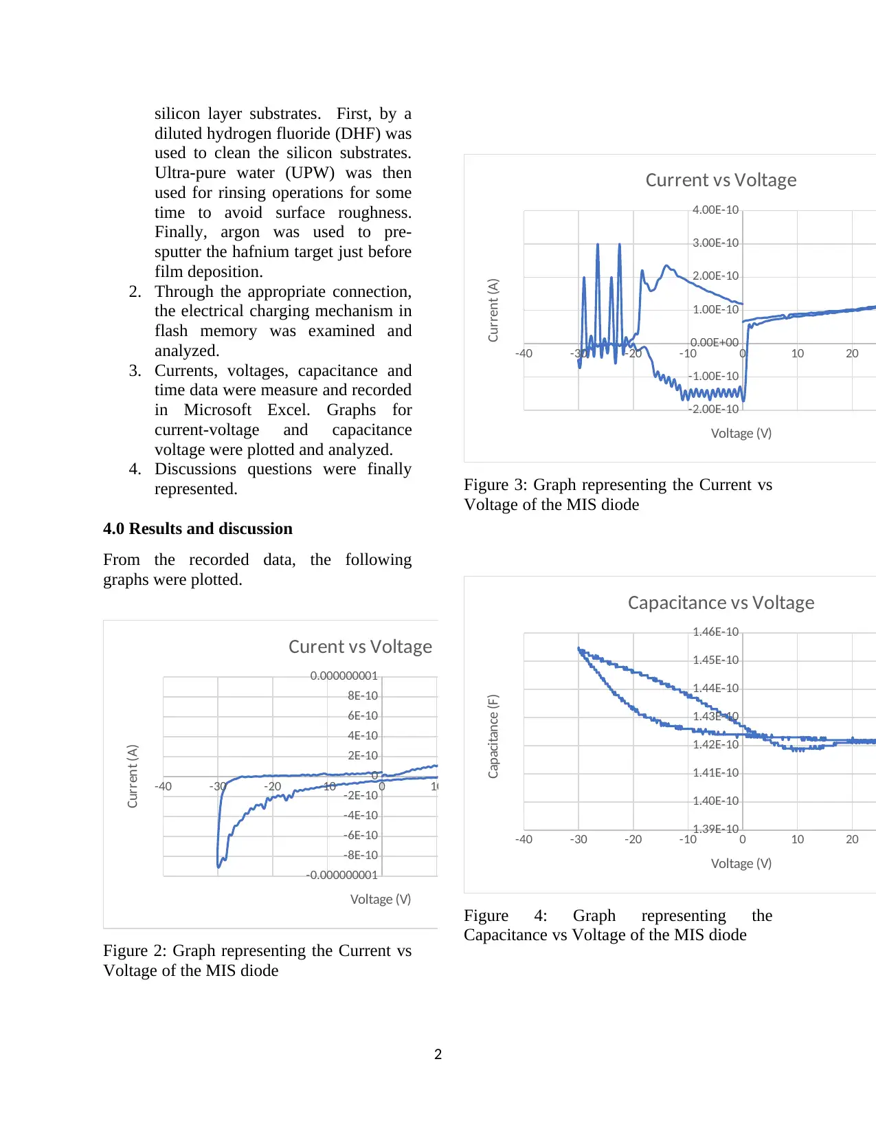
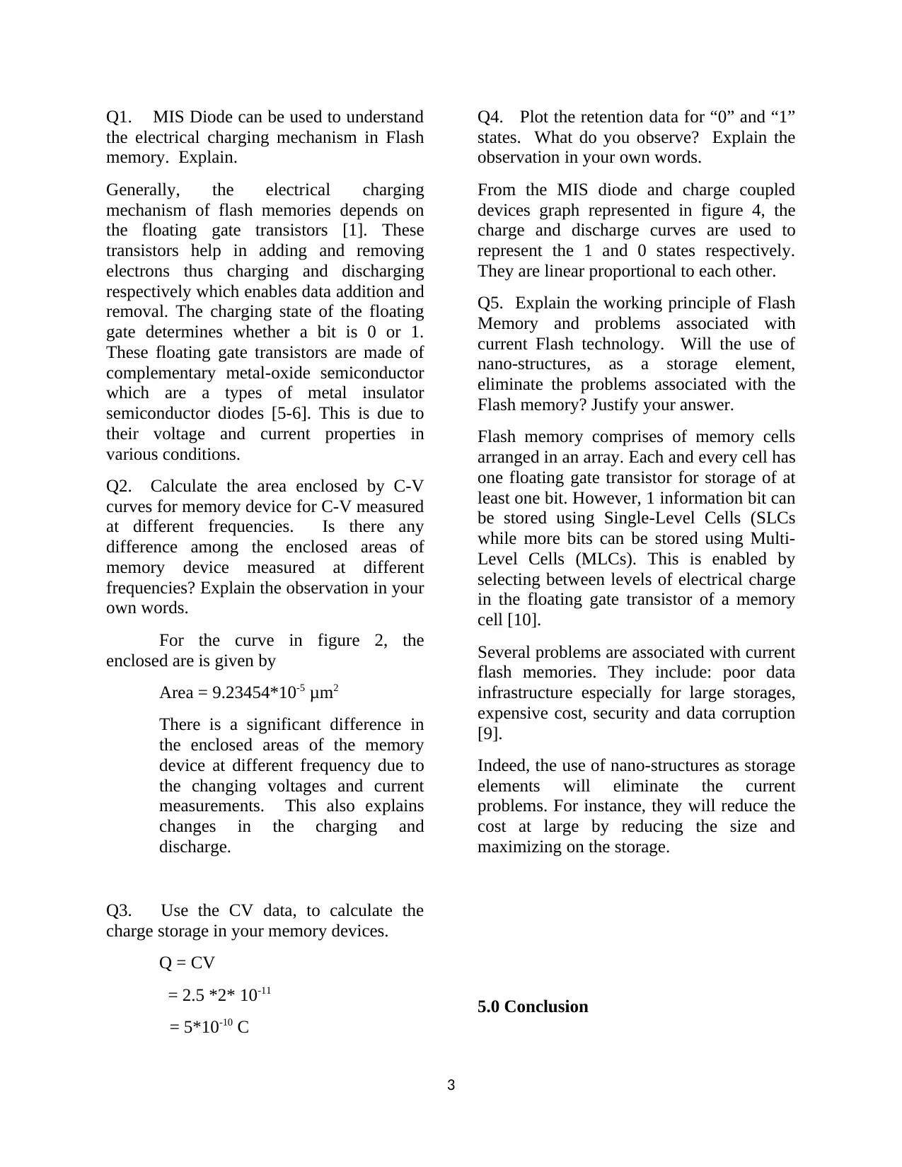
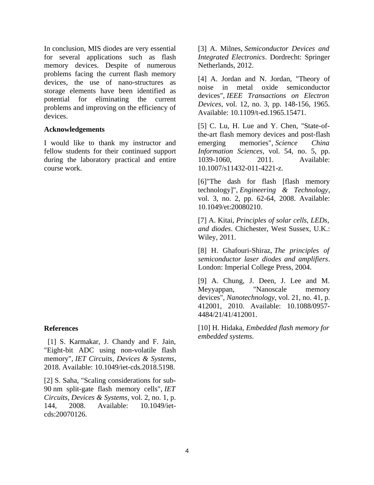
This report investigates the application of Metal-Insulator-Semiconductor (MIS) diodes in the electrical charging mechanism of flash memory. It begins by introducing the significance of diodes in various electronic components and highlights the stability and reliability of MIS diodes in semiconductor research. The experimental section details the fabrication process of MIS diodes on silicon substrates and the procedures for examining the electrical charging mechanism in flash memory, including data measurement and analysis. The results and discussion section presents current-voltage and capacitance-voltage graphs, addressing key questions about the role of MIS diodes in flash memory, charge storage calculations, and the impact of nanostructures on flash memory technology. The report concludes by emphasizing the essential role of MIS diodes in flash memory devices and the potential of nanostructures to overcome current limitations. References to relevant research articles are also included, providing a comprehensive overview of the topic.
1 out of 4

Your All-in-One AI-Powered Toolkit for Academic Success.
+13062052269
info@desklib.com
Available 24*7 on WhatsApp / Email
![[object Object]](/_next/static/media/star-bottom.7253800d.svg)
Copyright © 2020–2025 A2Z Services. All Rights Reserved. Developed and managed by ZUCOL.