101CDE 2018/19: Analogue and Digital Electronics Assignment Solution
VerifiedAdded on 2023/04/24
|25
|2177
|288
Homework Assignment
AI Summary
This document presents a comprehensive solution to an Analogue and Digital Electronics assignment, addressing key concepts in semiconductor devices and circuit design. The assignment covers the PN junction, including doping elements, depletion zone formation, and diode characteristics, with circuit diagrams and voltage-current curves. It then delves into diode applications such as calculating current in a circuit and analyzing clipping and rectification circuits. The solution further explores Bipolar Junction Transistors (BJTs), including bias circuits, DC and AC models, and load line analysis. Finally, it examines Field Effect Transistors (FETs), including their semiconductor basics, DC and AC models, and voltage gain calculations for an amplifier circuit. The document concludes with a design task involving a BJT-based amplifier, including circuit design, simulation results, and voltage gain calculations. Works cited are also included.

Student
Instructor
Analogue and digital electronics
Date
Instructor
Analogue and digital electronics
Date
Paraphrase This Document
Need a fresh take? Get an instant paraphrase of this document with our AI Paraphraser
2
Section 1: PN Junction
1.1 Basic Semiconductor Concept
1.1.1
I. Boron
II. Aluminum
They all have 3 valence electrons (Laube).
1.1.2
I. Phosphorus
II. Antimony
They have 5 valence electrons (Laube).
1.2 PN junction (diode) basic
1.2.1
Depletion zone of P-N junction is formed by intimate contact between p-type and
n-type semiconductors such that crystal structure remains continuous at the boundary.
The junction has a transition of a very short thickness, 1micro, from p-type material to n-
type material. The p-type which forms the anode has acceptor atoms while n-type which
forms the cathode, has donor atoms. Majority carriers in p-type are holes while minority
charge carriers are electrons. Majority charge carriers through diffusion process, move
3
from high concentration region to a region of low concentration hence forming
concentration gradient. For n-type majority carriers are electrons while minority carriers
are holes. Positive and negative ions are immobile charge carriers. At the junction, holes
in p-type recombine with electrons in the n-type leaving only acceptor and donor
immobile ions in the depletion layer. When enough electrons have accumulated the p-
region, more electrons diffusing from n-region are repelled. A similar case for holes from
p-region diffusing to the n-region are repelled. The action leads to a state of equilibrium
with fixed immobile negative and positive ions at near the junction with no charge
carriers. Barrier voltage across the depletion layer barricades the movement of charge
carriers across the depletion layer (Nave).
1.2.2
The junction is forward biased by applying a positive voltage at the p-type and negative
voltage at the n-type, mobility majority charge carriers results to more flow of current as
a result of reduced depletion layer (Nave).
When reverse voltage is applied, a constant small reverse current flow due to mobility
of minority charge carriers as a result of increased depletion layer.
1.2.3
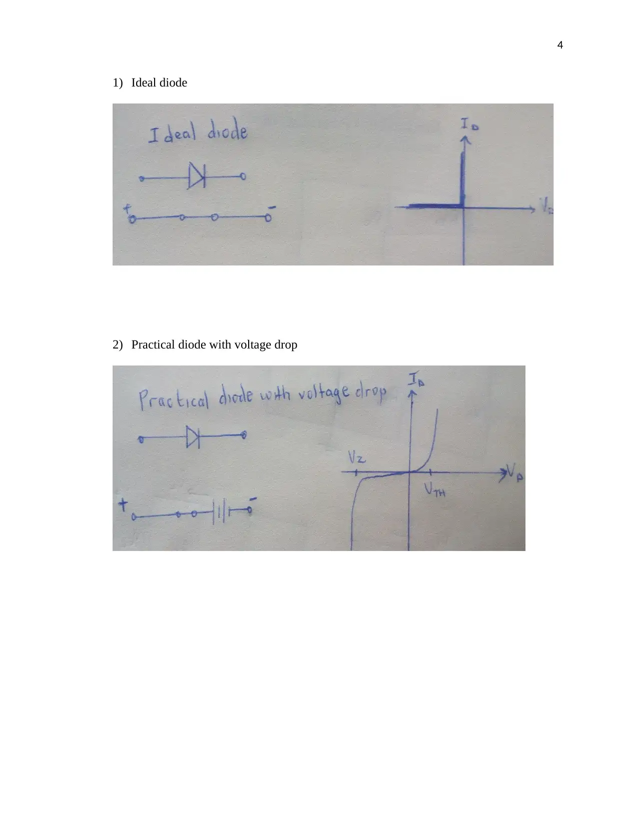
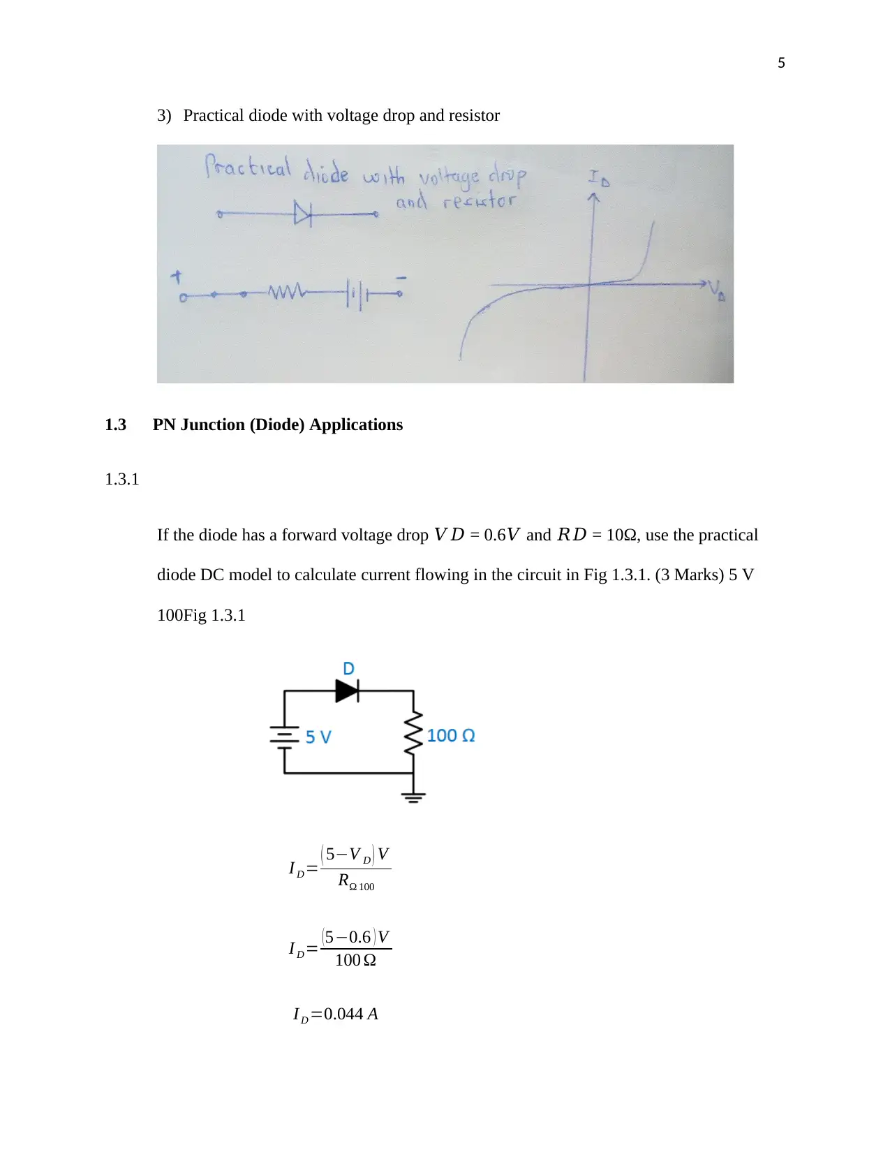
The ebullient circuits and corresponding Voltage verses Current curves of a diode when
considering it as 1) ideal diode, 2) practical diode with voltage drop, 3) practical diode
with voltage drop and resistance
⊘ This is a preview!⊘
Do you want full access?
Subscribe today to unlock all pages.

Trusted by 1+ million students worldwide
4
1) Ideal diode
2) Practical diode with voltage drop
1) Ideal diode
2) Practical diode with voltage drop
Paraphrase This Document
Need a fresh take? Get an instant paraphrase of this document with our AI Paraphraser
5
3) Practical diode with voltage drop and resistor
1.3 PN Junction (Diode) Applications
1.3.1
If the diode has a forward voltage drop 𝑉𝐷 = 0.6𝑉 and 𝑅𝐷 = 10Ω, use the practical
diode DC model to calculate current flowing in the circuit in Fig 1.3.1. (3 Marks) 5 V
100Fig 1.3.1
I D = ( 5−V D ) V
RΩ 100
I D = ( 5−0.6 ) V
100 Ω
I D =0.044 A
6
1.3.2
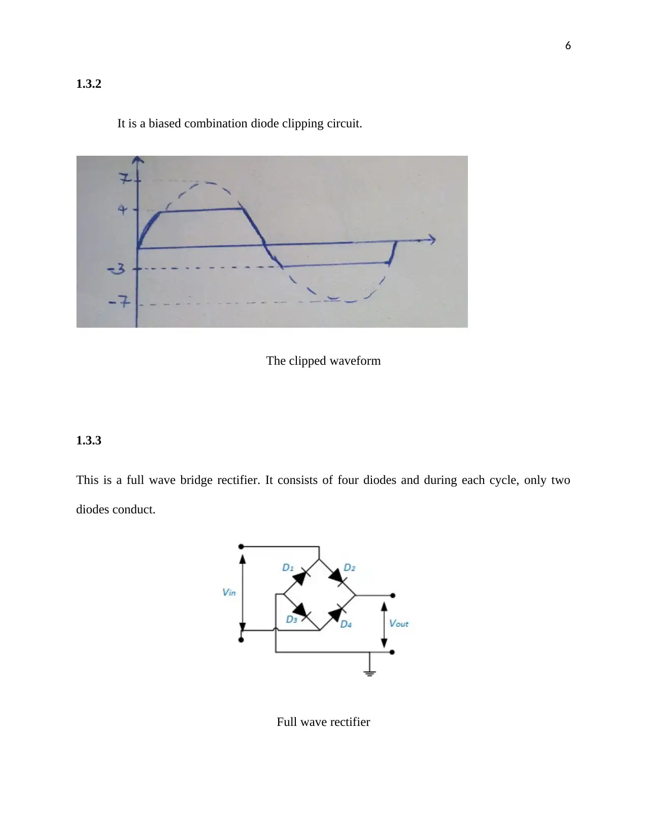
It is a biased combination diode clipping circuit.
The clipped waveform
1.3.3
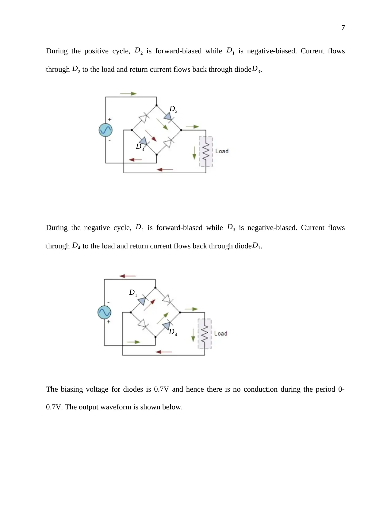
This is a full wave bridge rectifier. It consists of four diodes and during each cycle, only two
diodes conduct.
Full wave rectifier
1.3.2
It is a biased combination diode clipping circuit.
The clipped waveform
1.3.3
This is a full wave bridge rectifier. It consists of four diodes and during each cycle, only two
diodes conduct.
Full wave rectifier
⊘ This is a preview!⊘
Do you want full access?
Subscribe today to unlock all pages.

Trusted by 1+ million students worldwide
7
During the positive cycle, D2 is forward-biased while D1 is negative-biased. Current flows
through D2 to the load and return current flows back through diode D3.
During the negative cycle, D4 is forward-biased while D3 is negative-biased. Current flows
through D4 to the load and return current flows back through diodeD1.
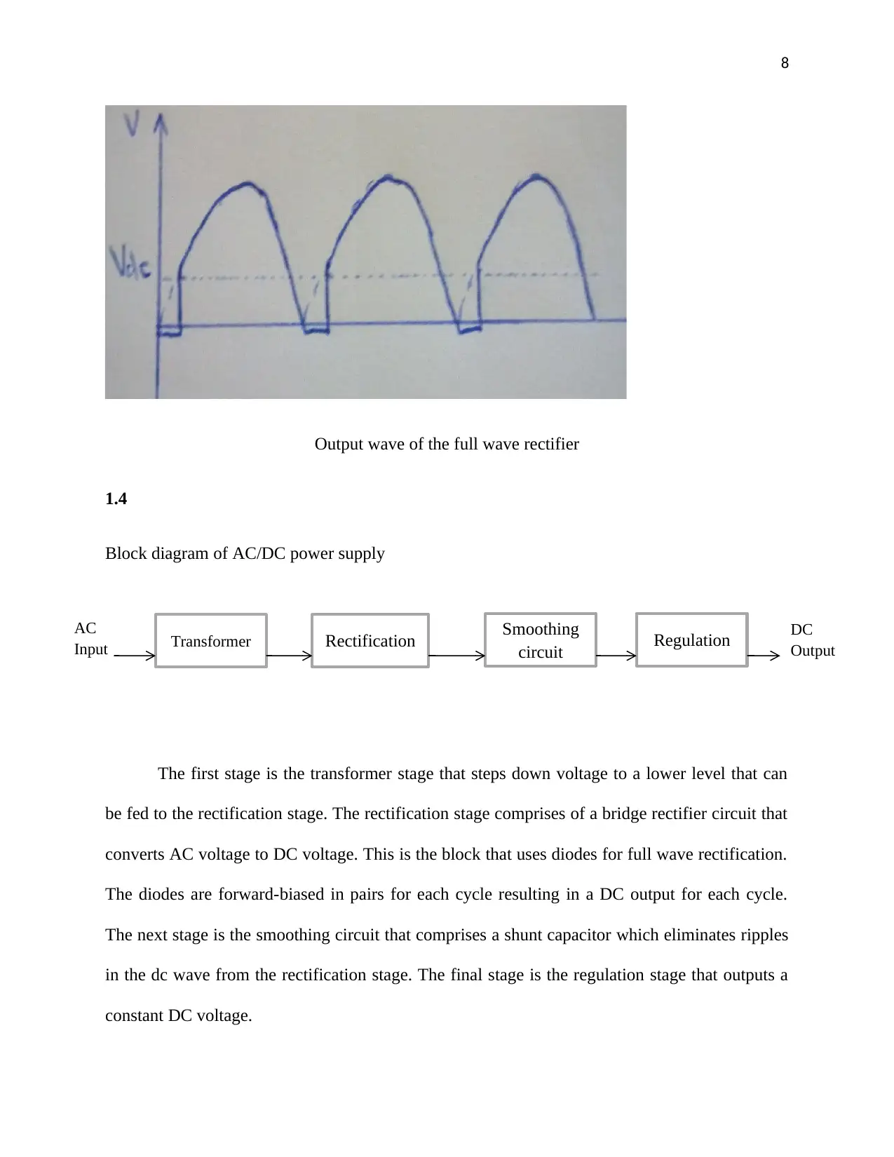
The biasing voltage for diodes is 0.7V and hence there is no conduction during the period 0-
0.7V. The output waveform is shown below.
D2
D3
D4
D1
Paraphrase This Document
Need a fresh take? Get an instant paraphrase of this document with our AI Paraphraser
8
Output wave of the full wave rectifier
1.4
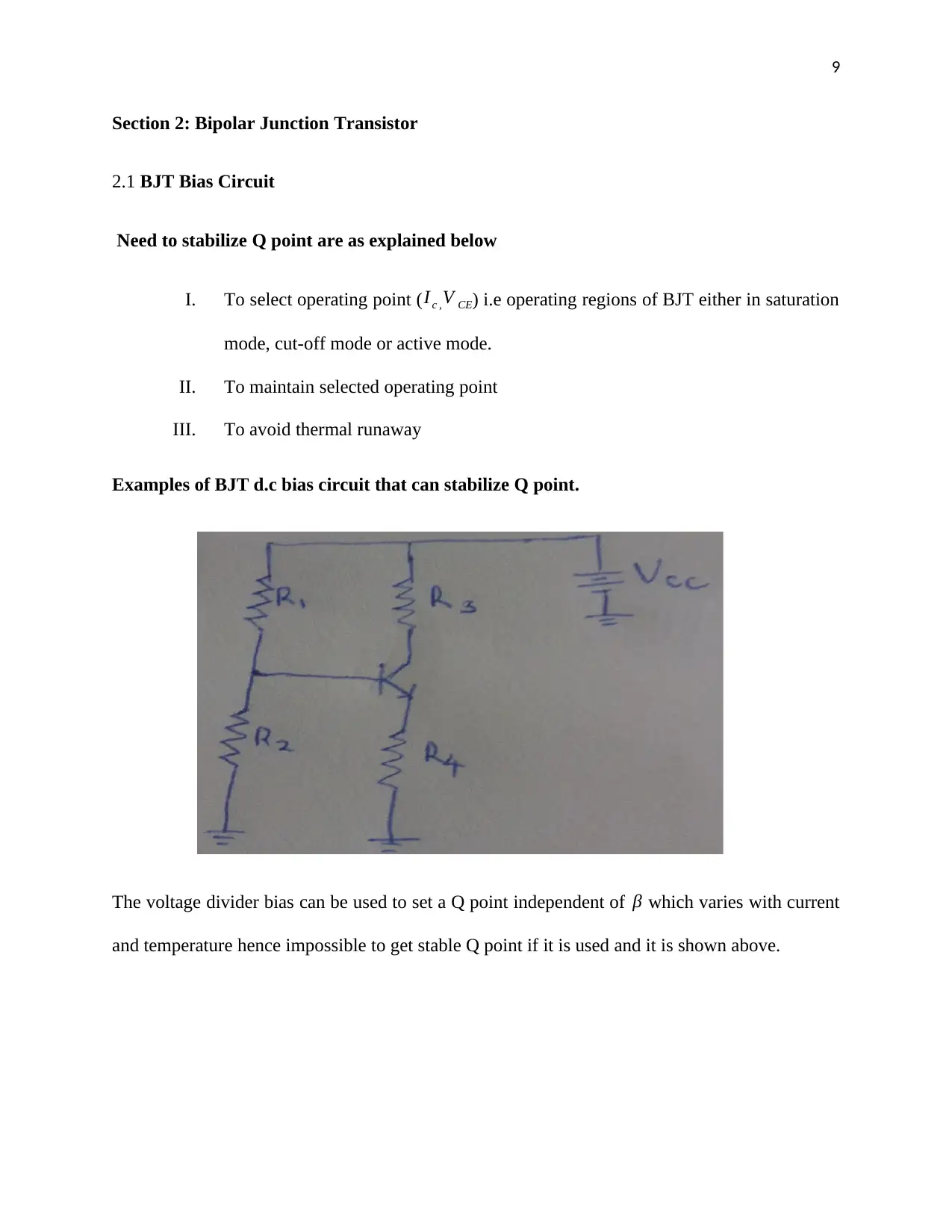
Block diagram of AC/DC power supply
The first stage is the transformer stage that steps down voltage to a lower level that can
be fed to the rectification stage. The rectification stage comprises of a bridge rectifier circuit that
converts AC voltage to DC voltage. This is the block that uses diodes for full wave rectification.
The diodes are forward-biased in pairs for each cycle resulting in a DC output for each cycle.
The next stage is the smoothing circuit that comprises a shunt capacitor which eliminates ripples
in the dc wave from the rectification stage. The final stage is the regulation stage that outputs a
constant DC voltage.
Transformer Rectification Smoothing
circuit Regulation
AC
Input
DC
Output
9
Section 2: Bipolar Junction Transistor
2.1 BJT Bias Circuit
Need to stabilize Q point are as explained below
I. To select operating point ( I c ,V CE) i.e operating regions of BJT either in saturation
mode, cut-off mode or active mode.
II. To maintain selected operating point
III. To avoid thermal runaway
Examples of BJT d.c bias circuit that can stabilize Q point.
The voltage divider bias can be used to set a Q point independent of β which varies with current
and temperature hence impossible to get stable Q point if it is used and it is shown above.
⊘ This is a preview!⊘
Do you want full access?
Subscribe today to unlock all pages.

Trusted by 1+ million students worldwide
10
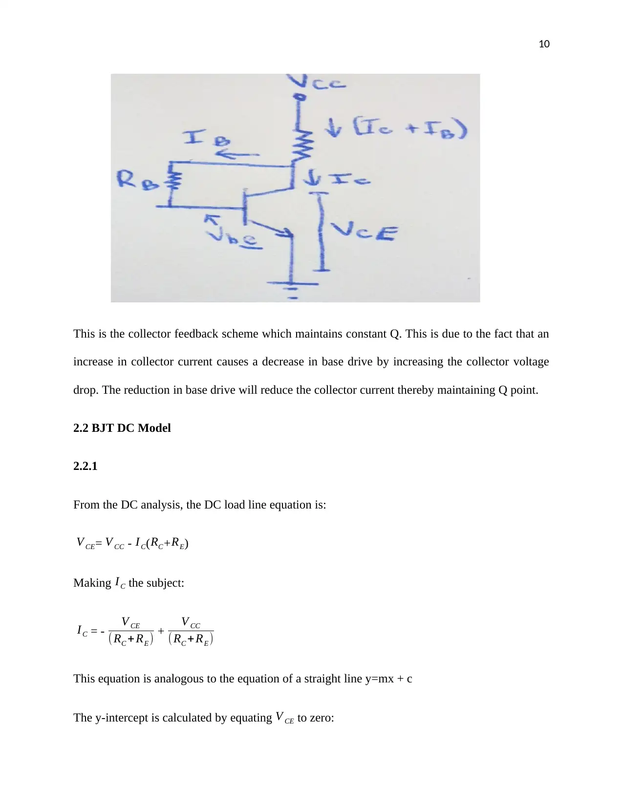
This is the collector feedback scheme which maintains constant Q. This is due to the fact that an
increase in collector current causes a decrease in base drive by increasing the collector voltage
drop. The reduction in base drive will reduce the collector current thereby maintaining Q point.
2.2 BJT DC Model
2.2.1
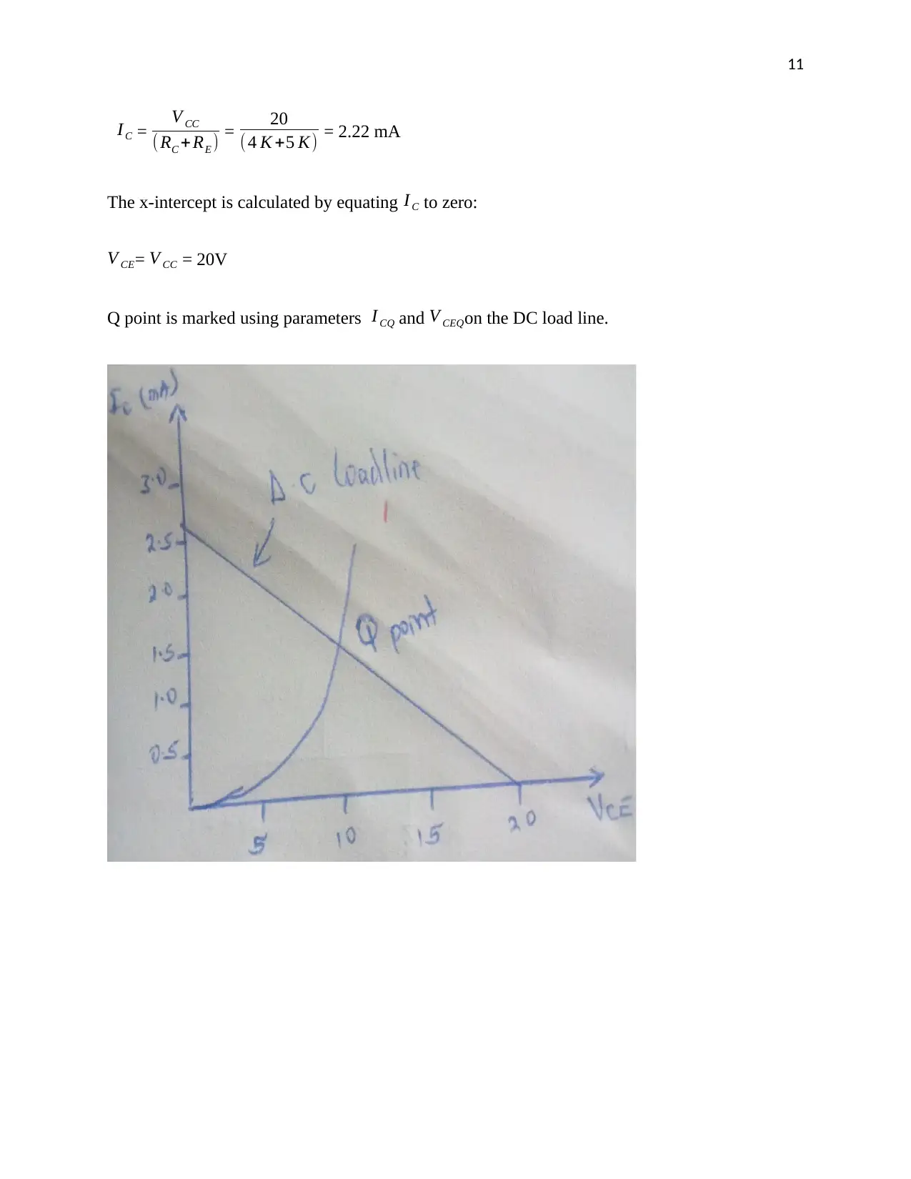
From the DC analysis, the DC load line equation is:
V CE= V CC - I C( RC + RE)
Making I C the subject:
I C = - V CE
( RC + RE ) + V CC
( RC +RE )
This equation is analogous to the equation of a straight line y=mx + c
The y-intercept is calculated by equating V CE to zero:
Paraphrase This Document
Need a fresh take? Get an instant paraphrase of this document with our AI Paraphraser
11
I C = V CC
( RC + RE ) = 20
( 4 K +5 K) = 2.22 mA
The x-intercept is calculated by equating I C to zero:
V CE= V CC = 20V
Q point is marked using parameters I CQ and V CEQon the DC load line.
I C = V CC
( RC + RE ) = 20
( 4 K +5 K) = 2.22 mA
The x-intercept is calculated by equating I C to zero:
V CE= V CC = 20V
Q point is marked using parameters I CQ and V CEQon the DC load line.
12
2.2.2
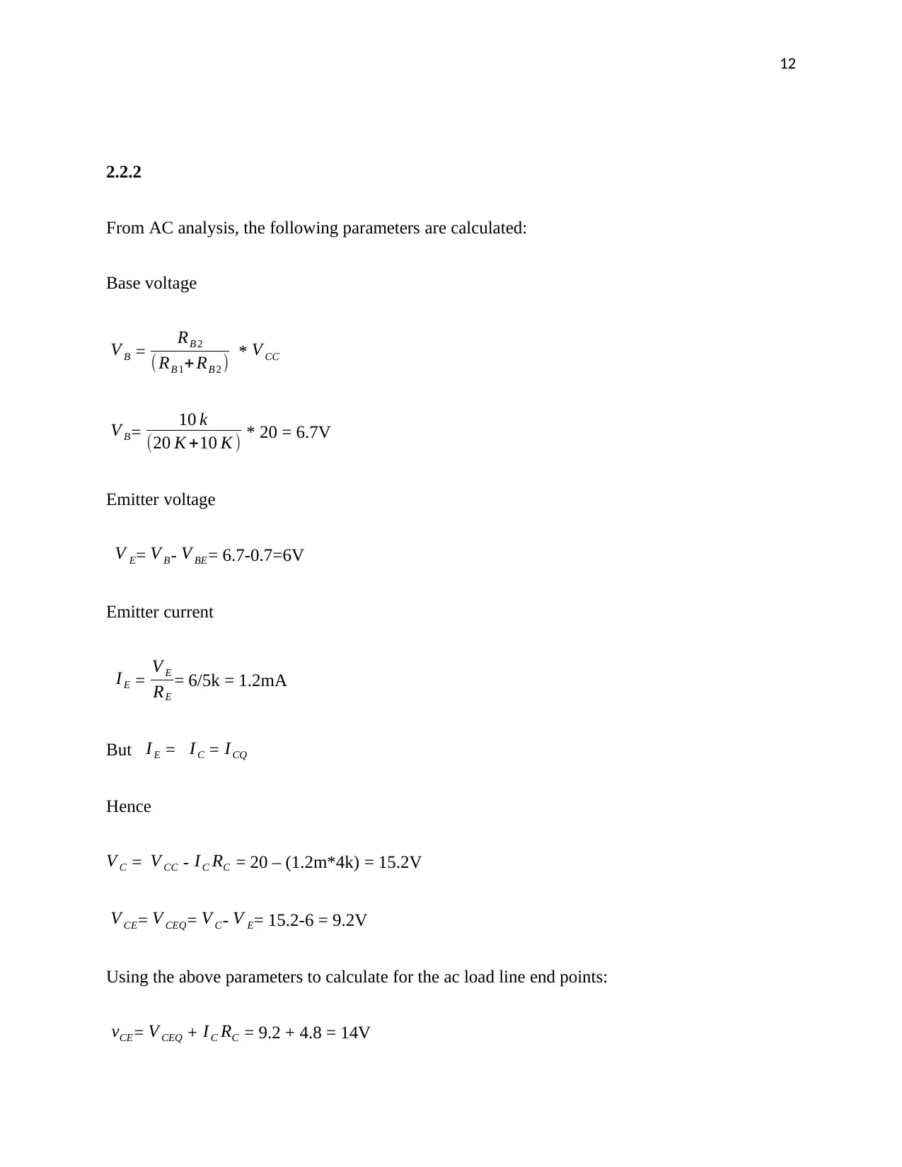
From AC analysis, the following parameters are calculated:
Base voltage
V B = RB 2
( RB 1+RB 2 ) * V CC
V B= 10 k
(20 K +10 K ) * 20 = 6.7V
Emitter voltage
V E= V B- V BE= 6.7-0.7=6V
Emitter current
I E = V E
RE
= 6/5k = 1.2mA
But I E = I C = I CQ
Hence
V C = V CC - I C RC = 20 – (1.2m*4k) = 15.2V
V CE= V CEQ= V C- V E= 15.2-6 = 9.2V
Using the above parameters to calculate for the ac load line end points:
vCE= V CEQ + I C RC = 9.2 + 4.8 = 14V
⊘ This is a preview!⊘
Do you want full access?
Subscribe today to unlock all pages.

Trusted by 1+ million students worldwide
1 out of 25
Related Documents
Your All-in-One AI-Powered Toolkit for Academic Success.
+13062052269
info@desklib.com
Available 24*7 on WhatsApp / Email
![[object Object]](/_next/static/media/star-bottom.7253800d.svg)
Unlock your academic potential
Copyright © 2020–2025 A2Z Services. All Rights Reserved. Developed and managed by ZUCOL.


