Scanning Microscopy Honours: AFM and Raman Analysis Exam Solution
VerifiedAdded on 2022/08/25
|25
|5964
|27
Homework Assignment
AI Summary
This document provides a detailed solution to a Scanning Microscopy honours exam, focusing on Atomic Force Microscopy (AFM) and Raman Microscopy. The solution addresses various aspects of AFM, including the principles of operation, force-distance curves, different imaging modes (contact and tapping), cantilever properties, and calibration techniques. It explores the advantages and disadvantages of different AFM modes, such as Peak Force tapping, and delves into the calibration of AFM components. Additionally, the solution analyzes a research paper on determining the spring constant of AFM cantilevers. The Raman microscopy section covers the selection rules for Raman activity, the prevalence of Stokes scattering, and the information that can be obtained about a sample through Raman scattering. The solution also examines the advantages of carbon nanotube tips in AFM and techniques for determining tip diameter. This assignment is designed to provide a comprehensive understanding of scanning microscopy techniques and their applications.
Scanning microscopy
A. Scanning probe microscopy section (SPM)
Introduction
The atomic force microscope (AFM) is a scanning probe microscope with very-high-
resolution. AFM is used for imaging samples at nanoscale resolution. The AFM machine is
used for biomaterial characterization. Information about the AFM microscope will be used to
answer the following questions.
Questions
1. At approximately what distance would an AFM tip sense the repulsive
interatomic forces? (2 marks)
An AFM tip would detect the repulsive interatomic forces at small sample-tip
distances .Near the surface of a sample, a powerful repulsive force appears between
the sample particles and cantilever tip. The strong repellent forces arise due to sample-
tip interactions. When the repulsive force is prevalent, the tip and sample are
considered to be in contact ( Geng & Borodich et al., 2016).
2. It is relatively easy to make a cantilever with a spring constant low enough to sense
the forces between atoms, such as a cantilever made of aluminium foil that is 4 mm long
and 1 mm wide. However, AFM cantilever manufacturers do not make cantilevers that
large. They make them much smaller, typically 100 to 200 microns long and 20 to 50
microns wide. What is the reason for this? (4 marks)
The sharpness or bluntness of a tip significantly affects the side-way resolution of the AFM,
as the sample-tip interaction area depends on the tip radius. The radius of the apex of an
unused tapping mode tip is small to enhance resolution. Sharp tip achieves greater resolution
for the AFM image. AFM cantilever force sensing is based on the deflection of the cantilever
Paraphrase This Document
Need a fresh take? Get an instant paraphrase of this document with our AI Paraphraser
Scanning microscopy
beam. When the tip size is very large, the sample would be subjected to high pressing force
due to the cantilever deflection, thus causing sensing error (Zhao & Hu et al., 2013).
3. How is the force the AFM tip exerts on the sample surface related to its deflection or
bending? (1 marks)
The degree of cantilever deflection is based on the force exerted by AFM tip. The higher the
force, the greater the deflection ( Geng & Borodich et al., 2016).
4. What are the disadvantages of contact mode compared to tapping mode? (4 marks)
The cantilever tip drags across the sample in contact mode .Dragging of the cantilever causes
frictional and adhesive forces. Contact mode thus causes sample damage and image data
distortion. Tapping mode AFM prevents frictional damage to sample by intermittently making
contact with sample surface. Images by Tapping mode AFM show no alteration and better
resolution (Al-Rashdi & Hilal et al. ,2012).
5. What is kept constant during imaging in tapping mode? (1 mark)
Cantilever frequency or oscillation amplitude (Proksch & Yablon, 2012).
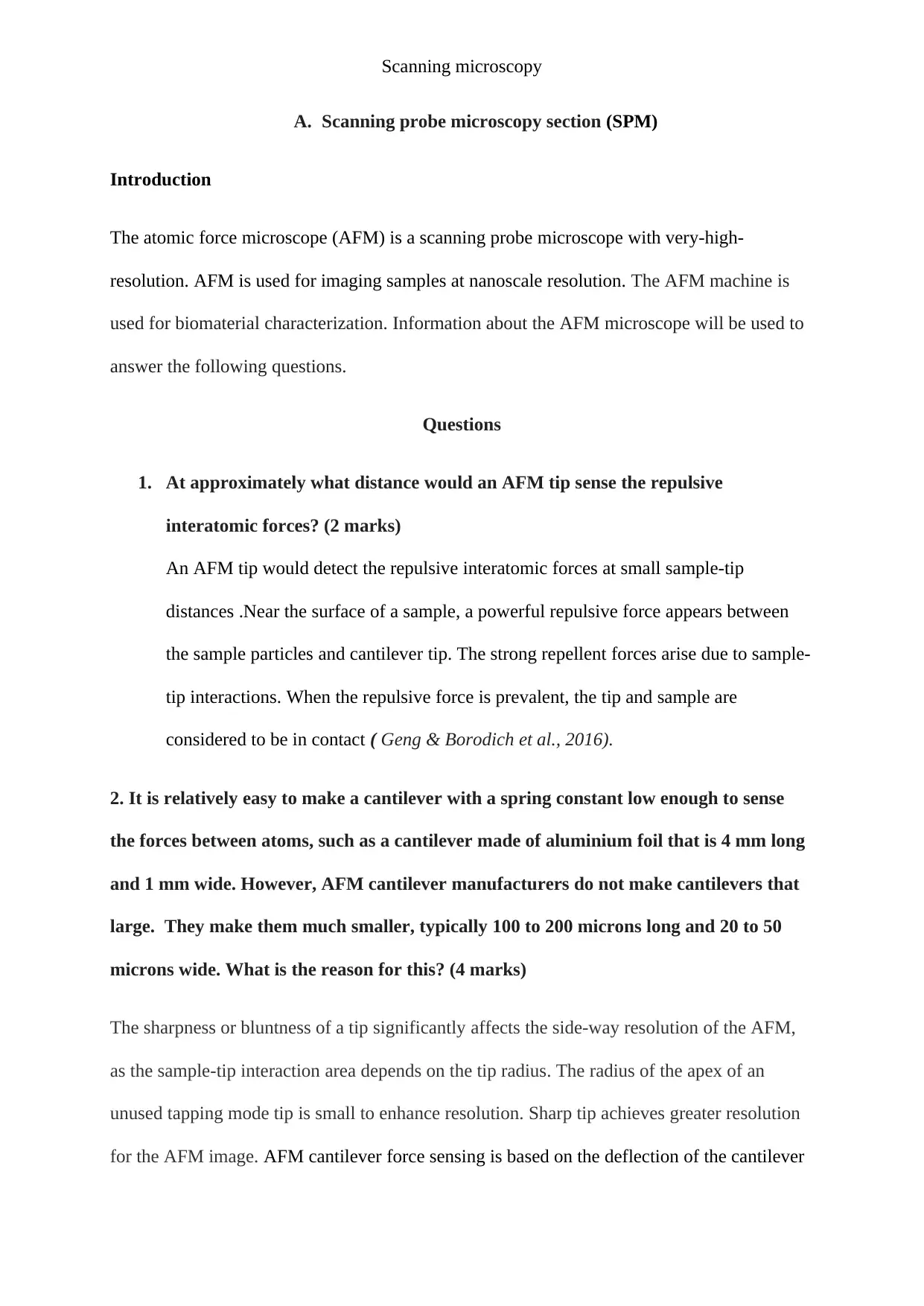
6. Figure 2 below Shows a typical resonance curve for an AFM tapping mode cantilever.
beam. When the tip size is very large, the sample would be subjected to high pressing force
due to the cantilever deflection, thus causing sensing error (Zhao & Hu et al., 2013).
3. How is the force the AFM tip exerts on the sample surface related to its deflection or
bending? (1 marks)
The degree of cantilever deflection is based on the force exerted by AFM tip. The higher the
force, the greater the deflection ( Geng & Borodich et al., 2016).
4. What are the disadvantages of contact mode compared to tapping mode? (4 marks)
The cantilever tip drags across the sample in contact mode .Dragging of the cantilever causes
frictional and adhesive forces. Contact mode thus causes sample damage and image data
distortion. Tapping mode AFM prevents frictional damage to sample by intermittently making
contact with sample surface. Images by Tapping mode AFM show no alteration and better
resolution (Al-Rashdi & Hilal et al. ,2012).
5. What is kept constant during imaging in tapping mode? (1 mark)
Cantilever frequency or oscillation amplitude (Proksch & Yablon, 2012).
6. Figure 2 below Shows a typical resonance curve for an AFM tapping mode cantilever.
Scanning microscopy
a. Define what resonance frequency means in terms of an AFM cantilever (2 marks)
The cantilever resonance frequency is the frequency at which the oscillation amplitude
reaches maximum energy. Mathematically, cantilever resonance frequency is the square root
of its spring constant divided by its mass ( Tsou & Proksch et al., 2011).
b. Determine the approximate Q factor for the resonance curve in figure 2 (The
resonance curve is in an attached excel file called Figure 2) (4 marks)
Q = F0/F3Db ; F0=300
Q = 300/5×3=20Hz/E
⊘ This is a preview!⊘
Do you want full access?
Subscribe today to unlock all pages.
Trusted by 1+ million students worldwide
Scanning microscopy
7. Why is the spring constant and resonant frequency for tapping mode probes much
larger, compared to contact mode probes when operating in air? (Hint: capillary layer)
(4 marks)
Van der Waals and capillary forces are involved during the application of AFM tapping mode
in an air tip-sample.Capillary force is due to water layout coating sample surface and the
cantilever tip.Repulsive force arise due to the contact between the tip and the sample.
Capillary force develops as the tip approaches the sample (Kavousi & Ebrahimi et al., 2011).
The capillary force is due to interactions between water films and the sample. As separation
reduces below a distance of the beginning of the capillary, a liqued column is established.
Retraction of the tip from the surface forms a meniscus and neck which breaks above a
critical distance ( Lauke & Heinrich et al. , 2014).
8. What information about the sample surface can force-distance curves potentially
give? (2 marks)
AFM topography images give information on overall surface morphology, can reveal defects,
and distinguish amorphous and crystalline phases, and identify nucleation and growth modes
(Liu & Wang, 2010).Additionally, images can be analysed to calculate areal surfaces
roughness parameters such as Sa (3D roughness average) and Sq (root mean square
roughness) or statistics on grain and domain size (Alsteens & Müller, 2013). Furthermore,
individual line sections can be used to determine step heights, film thickness, and even lattice
spacings (Waltman & Guo, 2012).
9. The company, called Bruker corporation, has developed an imaging mode called Peak
Force tapping. What are the advantages of this imaging mode compared to other
imaging modes? (3 marks)
Paraphrase This Document
Need a fresh take? Get an instant paraphrase of this document with our AI Paraphraser
Scanning microscopy
Tapping mode AFM does not drag tip on hence less surface alteration. Measurements with
tapping mode are achievable in ambient conditions. Tapping mode has high resolution of
samples than contact mode (Proksch & Walters et al., 2014).
10. What does calibration mean? Why is calibration such an important part of any
experiment? (3 marks)
The procedure of comparing reading on one piece of equipment or system, with another piece
of equipment that has been calibrated and referenced to a known set of parameters is called
calibration. The reference equipment should directly be in match with international standards
(Kelly & Sukhatme, 2011). Equipment calibration is conducted to check the accuracy and
quality of measurements recorded. Equipment tend to have drifted accuracy when measuring
specific parameters such as temperature and humidity ( Bolgen & Christiansen et al., 2010).
Calibrated equipment gives confident, reliable and repeatable result (Savescu & Laba, 2016).
11. In order to accurately measure quantitative forces using AFM what components of
the microscope must be calibrated? (4 marks)
AFM microscope has parts that need to be calibrated for accurate measurements of data
(Müller & Dufrene, 2010). The AFM components that are calibrated include:
i) cantilever sensor ii) Laser diode iii) Photodiode
iv) Sensitive photo-detector v) Probe tip vi) computer
12. Describe a technique to calibrate the cantilever deflection of an AFM cantilever.
Give advantages and disadvantages of the technique. (4 marks)
Scanning microscopy
Calibration of cantilever deflection of an AFM cantilever can be done by various techniques
such as thermal noise method, Static response techniques, Dynamic response method, the
piezolever method, e.t.c. The piezolever method is described below.
Piezolever method of calibrating AFM cantilever
Calibration designed apparatus are used to calibrate AFM cantilevers. Designed calibrated
apparatus is rested on the AFM stage. Optical microscope of the AFM locates the
piezolever.AFM cantilever is brought very close to the piezolever. The cantilever is aligned
above the piezolever (Kilpatrick & Thorén et al., 2016). Piezolever and cantilevers are brought
into contact using and AFM software. The voltage output from the piezolever is reset to zero.
This procedure is repeated until the AFM cantilever tip is in contact with the reverse side of
the piezolever tip. After a successful connection is made, the base of the piezolever is moved
up using the manual control of the AFM stage. The change in voltage is recorded. This
process is repeated until sufficient data are collected (Crawford & Bieske et al., 2012).
13. . Read the following paper carefully and answer the following
questions13a to 13c
(DOI: 10.1063/1.1144209, Authors: J. P. Cleveland, S. Manne, D. Bocek and P. K.
Hansma)
A non destructive method for determining the spring constant of cantilevers for
scanning force microscopy.
a. Describe the sources of error for this method? (4 marks)
The accuracy of force acting between a sample and an AFM cantilever is determined by the
spring constant of the AFM cantilever. Change in the resonant frequency of a cantilever is
measured by Cleveland method. Microspheres of known mass values are attached near the
free end of the cantilever. The errors encountered are due to deviations in cantilever shape,
presence of surface coating materials on a cantilever and substandard calibration methods.
Additionally, the error source lies with the estimation of the added mass, which depends
⊘ This is a preview!⊘
Do you want full access?
Subscribe today to unlock all pages.
Trusted by 1+ million students worldwide
Scanning microscopy
mostly on the measurement of the diameter of the spherical mass added (Chiesa & Thomson et
al. , 2012).
b. Why is it best to use Tungsten or gold spheres as the added mass? (2 marks)
The advantages of tungsten or gold microspheres include high-density, low thermal expansion
and corrosion-resistance thus can be used in a range of corrosive environments ( Cleveland &
Manne, 1993)
c. A sphere made of pure gold with a diameter of 10 microns is attached to the end of an
AFM cantilever. The cantilever has an initial resonant frequency of 10 kHz, and a
resonant frequency of 8 kHz after the sphere is attached. What is the spring constant of
the cantilever? Do not just write down the answer also describe how you calculated the
answer. (Big hint: Use the first of the equations marked as (5) in the paper) (4 marks)
Initial resonant frequency, f1 = 10kHz
New resonant frequency,f2 =8
Lenth of the gold sphere is 10 microns
K = 2∏3l 3√v03
K = (2×3.1423 ×103 √103
K = 1.962×10⁶
14. When imaging a carbon nano-tube sample using AFM, the measured height of the
nano-tubes is typically much smaller than the measured width. Why? (3 marks)
Smaller height reduces the exerted force on sample surface
Paraphrase This Document
Need a fresh take? Get an instant paraphrase of this document with our AI Paraphraser
Scanning microscopy
15. Describe 2 techniques you could use to determine the diameter of an AFM tip. What
advantages and disadvantages do they have? (6 marks)
The two techniques for tip size measurement are Capacitance method and
Minimum critical amplitude. In minimum critical amplitude, the cantilever is oscillated at a
fixed frequency and the oscillation amplitude is used as feedback parameter to measure the tip
radius and size.
the cantilever is oscillated at a
xed frequency
(usually at its natural
frequency) and the oscillation
ampli-
tude is used as a feedback
parameter to recover the
sample
topog
Advantages of Minimum critical amplitude include: more accurate for
relatively sharp tips and less time consuming, technique can be used with
any type of tip. The disadvantage of critical minimum is that tip is prone to
damage.
The capacitance method, on the other
hand, is more time-consuming and less versatile compared to
The advantage of Capacitance method is reduced damage to the tip is due
to no mechanical contact with the sample.Disadvantages include: time
Scanning microscopy
consuming, It is less versatile and it is much involving since it involves alot
of procedures (Stefancich & Chiesa et al., 2014).
16. What advantages do carbon nanotubes tips have in comparison to standard silicon
or silicon nitride tips? (3 marks)
Carbon-nanotubes (CNTs) tips are less brittle and does not wear out easily. CNTs can
transmit large forces. Silicon tips are brittle and easily break. Silicon tips tend to fracture
much easier as they become sharper and narrower.
B. Raman microscopy section
1. What is the selection rule for a molecule or material to be Raman active? (3 marks)
A molecule or material is Roman active when its polarizability changes during vibrational
motion. Polarizability refers to the charge distribution. A molecule distortion is caused by
distribution of charge from an external electric field e.g. electromagnetic wave. The more
changes in the electron cloud geometry, the higher the polarizability (Dawson & Hoffman et
al. ,2010).
2. Why are most Raman microscopes based on Stokes scattering? (2 marks)
Scattering of radiation by stokes is more intense. This is due to very few molecules getting to
the exciting level. The laser light in stoke scattering is very intense beam of nearly
monochromatic light that interacts with sample molecules. When the radiation is absorbed, a
molecule jumps to a higher vibrational energy level. When the molecule relaxes back to a
lower energy level, radiation is emitted.
3. What information about a sample can Raman scattering potentially give? (5 marks)
⊘ This is a preview!⊘
Do you want full access?
Subscribe today to unlock all pages.
Trusted by 1+ million students worldwide
Scanning microscopy
Sample information revealed by Roman scattering include identity of minerals and organic
substances. Chemical formulas and the arrangements of the atoms within these minerals and
organic substances are established. Chemical compositions of a compound such as cation ratio
and energies of molecular vibrations and rotations are known. Molecular vibrations depend
on the particular atoms or ions that comprise the molecule. Chemical bonding and molecule
structure are revealed by Raman scattering.
4. What is Rayleigh scattering? What problem does it pose for Raman scattering? How
can it be counteracted? (6 marks)
Rayleigh is an elastic light scattering phenomenon. Scattering by Raman is inelastic light
scattering phenomenon. In Rayleigh scattering matter involved does not gain or lose energy in
the process. The scattered light has the similar frequency to the radiation from which it
emanated. Atoms involved in Raman scattering can either gain or lose energy. The resultant
light thus has either a lower or higher frequency. Rayleigh backscattering limits the sensitivity
improvements that can be realized by Raman scattering. The remedy to the backscattering of
Rayleigh is achieved by removing rejection filters and installing monochromatic lasers
5. Why is it an advantage to have a Raman microscope with a range of excitation
wavelengths (e.g., 532 nm, 633 nm, and 785 nm) (5 marks)
Fluorescence of a material is dependent on the excitation wavelength. The longer the
wavelength of a laser, the weaker fluorescence. Additionally, the detector is also reliant on the
light wavelength. A range of excitation wavelength solves the problem of photoluminescence
and profits resonance conditions from the analysed material and the supporting substrate.
Different excitation wavelength limits the noise level and yields a Raman spectrum with a
superior signal to vibrational ratio.The excitation frequency determines the Raman scattering
Paraphrase This Document
Need a fresh take? Get an instant paraphrase of this document with our AI Paraphraser
Scanning microscopy
as frequency of the light is inversely proportional to the wavelength. The Raman system with
variable excitation wavelength suppresses unwanted fluorescence signals.
6.
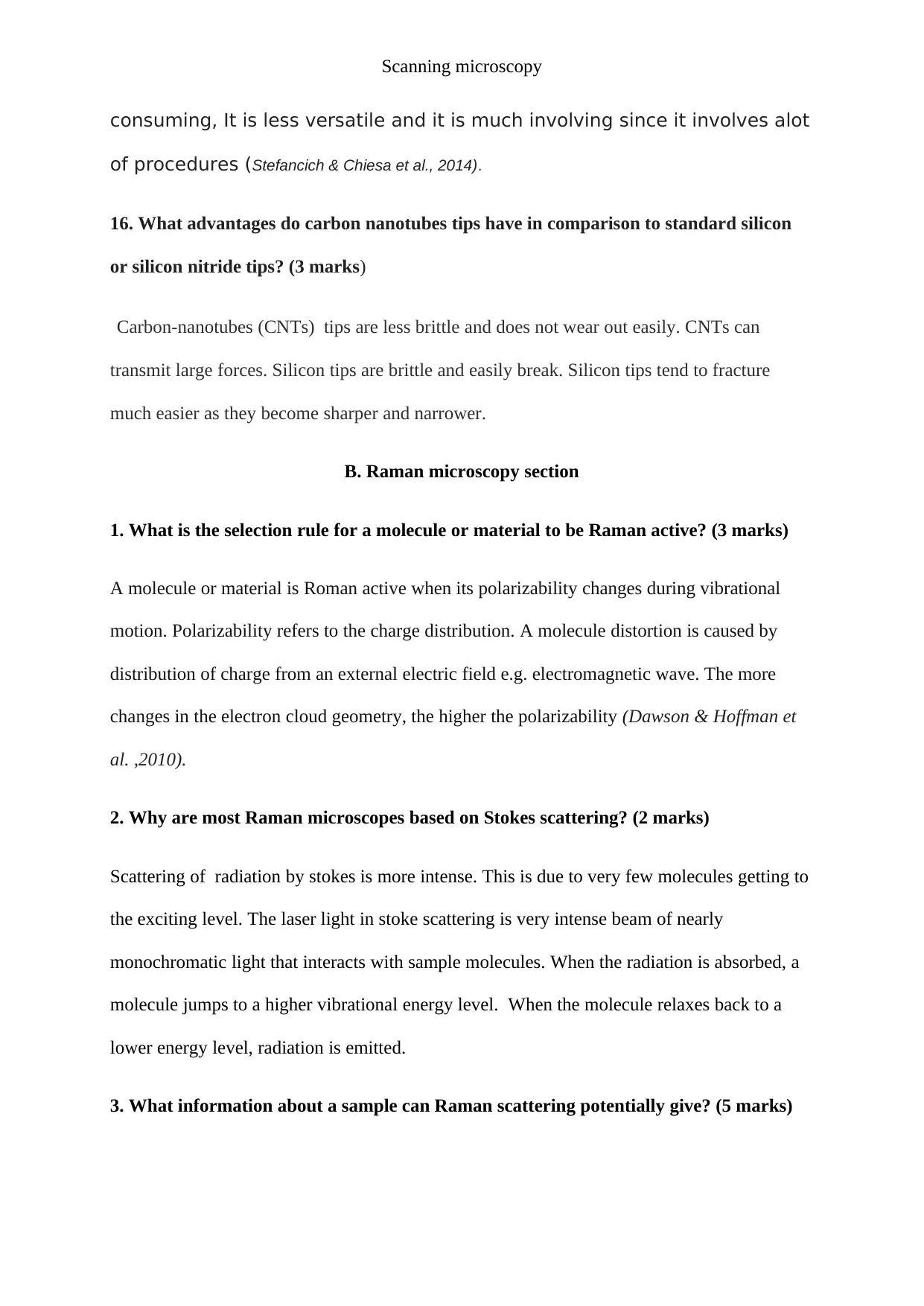
Figure 3. Raman spectrum of carbon nanotubes on silicon.
a. For peaks 1 to 7, assign which ones are for elastic scattering and which are for silicon
and carbon nanotubes. (7 marks)
Peak 1: carbon nanotubes Peak2: Silicon Peak3: Carbon nanotubes
Peak4: silicon Peak5: Silicon Peak6: carbon nanotubes
Peak7: Silicon
b. What are the typical names given for peaks 2,5,6 and 7? What information do they
give about the associated material? (8 marks)
Peak 2: Peak 5: Peak 6: D band
Peak 7:
Peaks 2, 5, and 7 shows that there are few defects associated with light scattering of
carbon nanotubes on silicon while Peak and 6 is associated with many defects.
7.
as frequency of the light is inversely proportional to the wavelength. The Raman system with
variable excitation wavelength suppresses unwanted fluorescence signals.
6.
Figure 3. Raman spectrum of carbon nanotubes on silicon.
a. For peaks 1 to 7, assign which ones are for elastic scattering and which are for silicon
and carbon nanotubes. (7 marks)
Peak 1: carbon nanotubes Peak2: Silicon Peak3: Carbon nanotubes
Peak4: silicon Peak5: Silicon Peak6: carbon nanotubes
Peak7: Silicon
b. What are the typical names given for peaks 2,5,6 and 7? What information do they
give about the associated material? (8 marks)
Peak 2: Peak 5: Peak 6: D band
Peak 7:
Peaks 2, 5, and 7 shows that there are few defects associated with light scattering of
carbon nanotubes on silicon while Peak and 6 is associated with many defects.
7.
Scanning microscopy
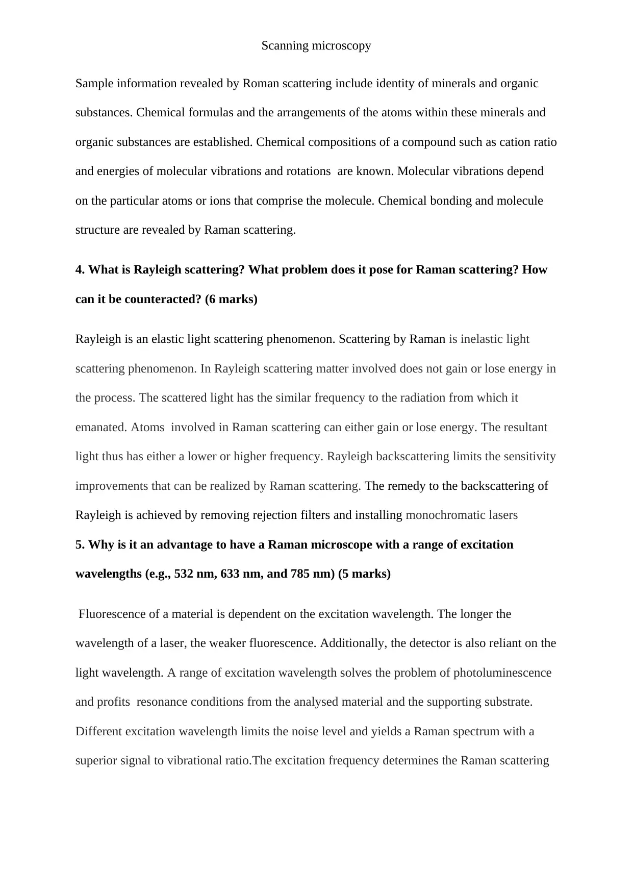
Figure 4.Raman spectrum of Graphene on silicon.
7. What information can peak 2 in figure 4 (at ~2680 wave-numbers and is known as the
2D band) give about the Graphene sample? (6 marks)
Peak 2 shows Graphene sample is contaminated.
8. Will the resolution of a Raman image using a 513 nm laser be better or worse than
using a 785 nm laser, assuming the same objective is being used? (2 marks)
Resolution of Raman image using a 513nm is better than resolution of 785.Raman scattering
efficiency increases with decrease in wavelength. Excitation efficiency is high with short
wavelength.
C. Electron microscopy section
1. What advantage does using electrons as the excitation source in a microscope have in
comparison with using optical light? (2 marks)
The use of a beam of electrons at a sample reveals biological and chemical structures. The use
of electrons to excite samples gives high magnification and resolution. An electron
⊘ This is a preview!⊘
Do you want full access?
Subscribe today to unlock all pages.
Trusted by 1+ million students worldwide
1 out of 25
Your All-in-One AI-Powered Toolkit for Academic Success.
+13062052269
info@desklib.com
Available 24*7 on WhatsApp / Email
![[object Object]](/_next/static/media/star-bottom.7253800d.svg)
Unlock your academic potential
Copyright © 2020–2026 A2Z Services. All Rights Reserved. Developed and managed by ZUCOL.