University Electrical Engineering: DC and AC Circuit Analysis Report
VerifiedAdded on 2022/11/19
|33
|3450
|288
Homework Assignment
AI Summary
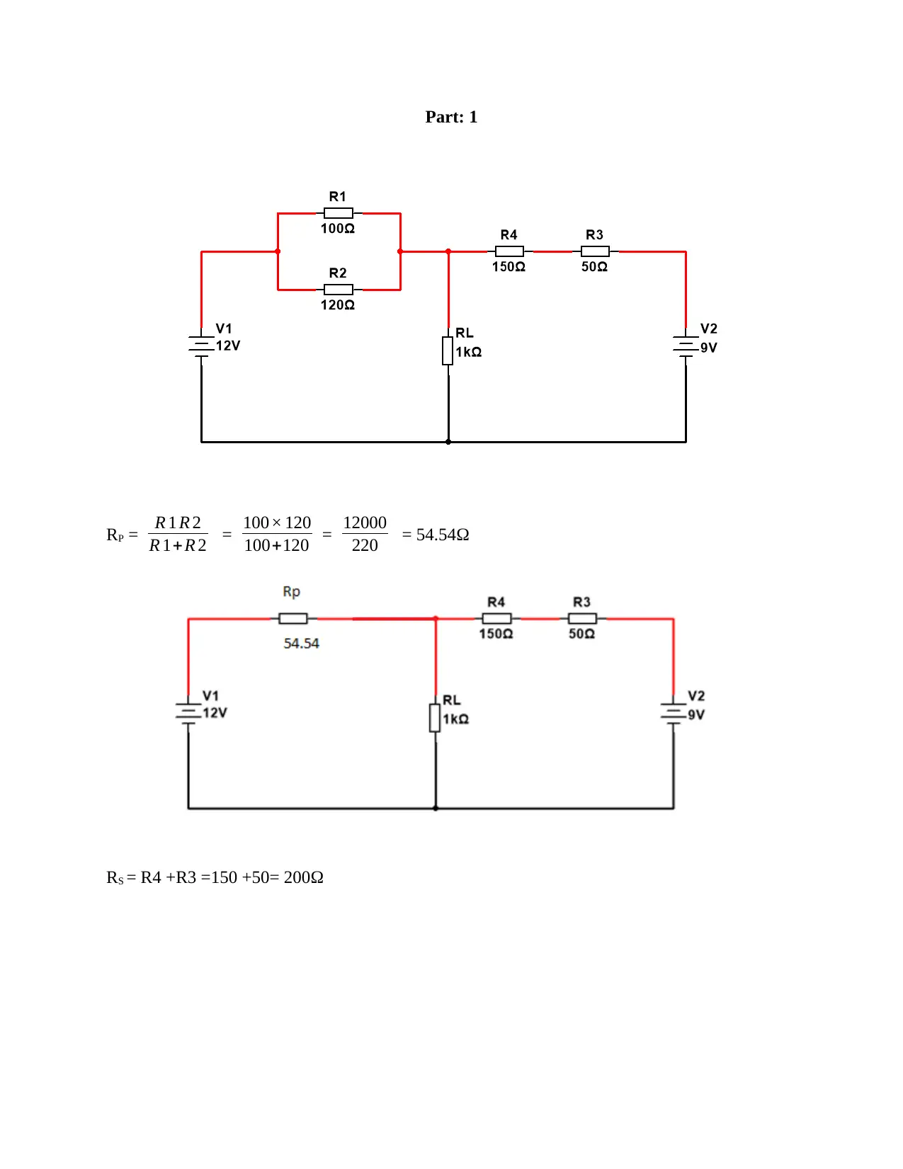
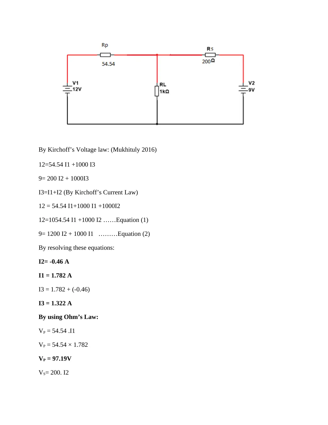
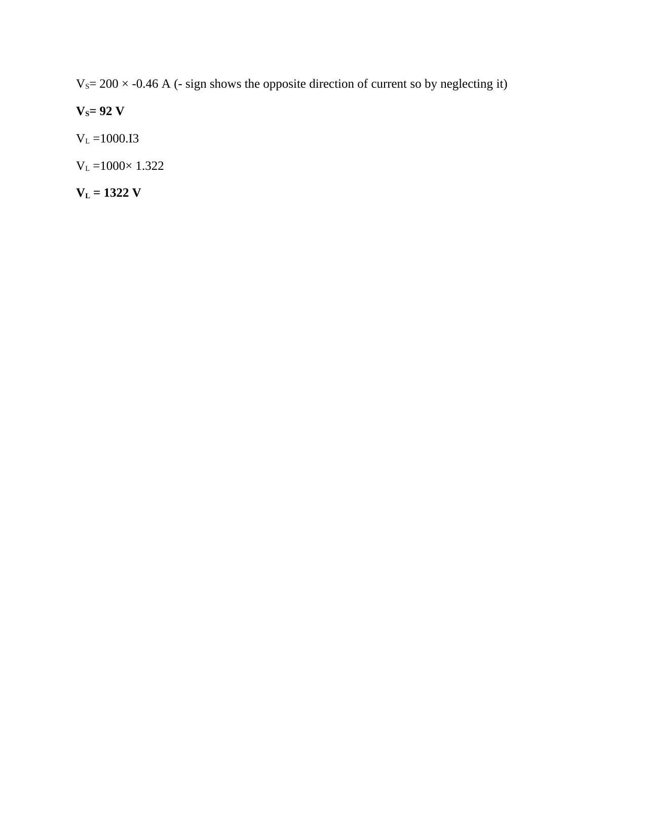
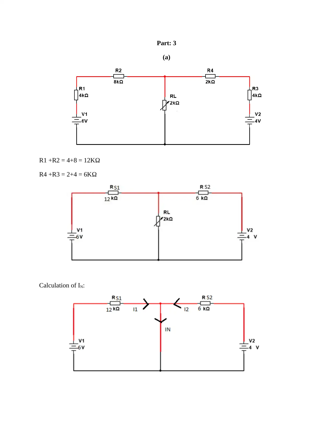
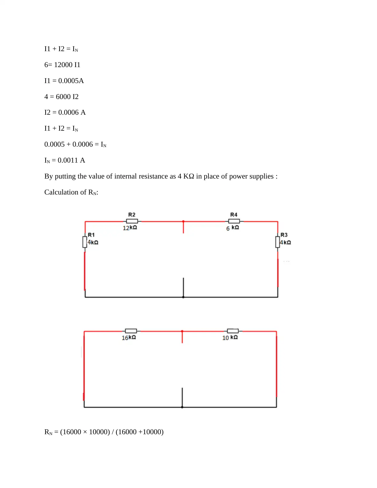
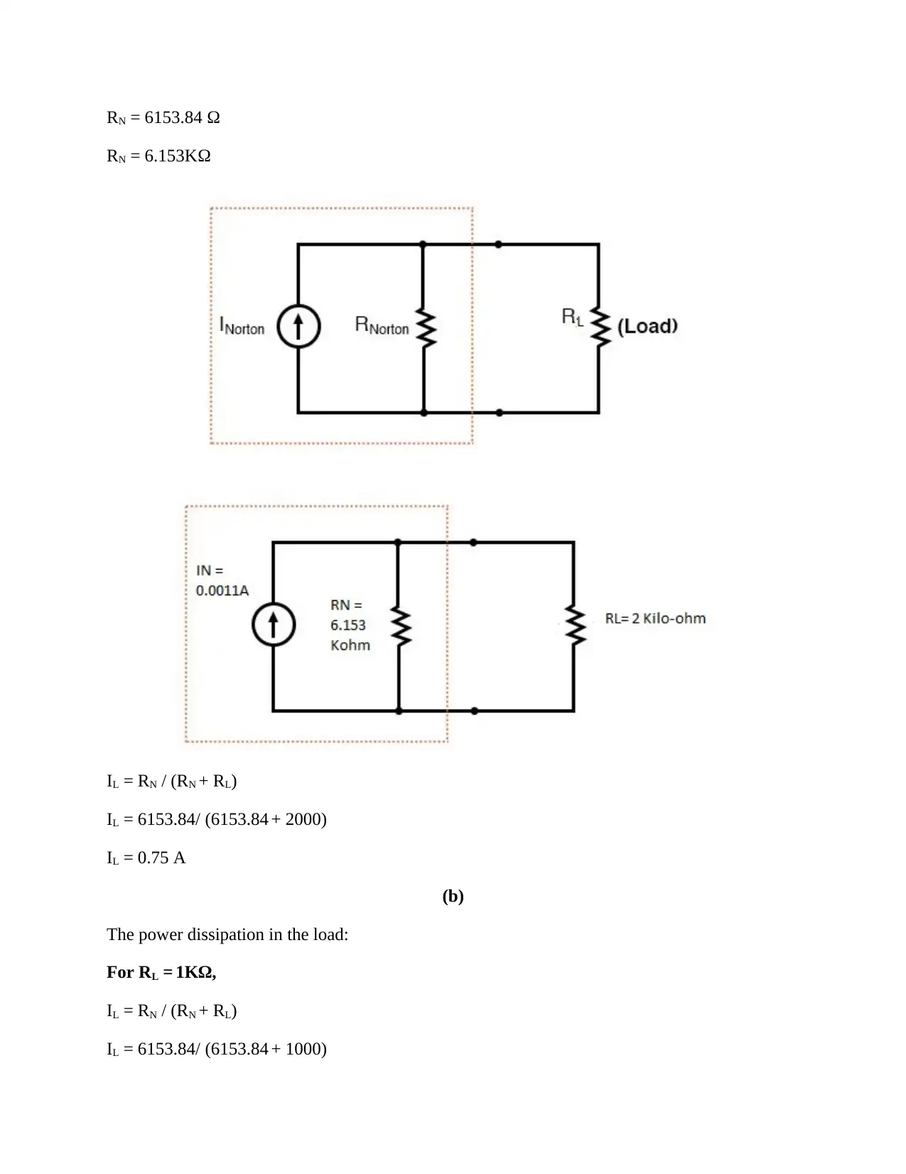
This assignment report presents a comprehensive analysis of DC and AC electrical circuits. The solution begins with an analysis of a DC circuit, applying Kirchhoff's and Ohm's Laws to determine voltage drops and currents. It then explores Thevenin's equivalent circuit. The report continues with an examination of various circuit components, including low-pass filters and resonant circuits, calculating impedance, current, voltage drops, and gain. The assignment also covers the principles of electromagnetic induction, explaining its applications. All calculations are presented with detailed working steps and Harvard referencing as required, ensuring a logical and coherent structure suitable for engineering analysis.

1 out of 33
Your All-in-One AI-Powered Toolkit for Academic Success.
+13062052269
info@desklib.com
Available 24*7 on WhatsApp / Email
![[object Object]](/_next/static/media/star-bottom.7253800d.svg)
Copyright © 2020–2026 A2Z Services. All Rights Reserved. Developed and managed by ZUCOL.