Chip Impedance Matching for UHF RFID Tag Antenna Design Project
VerifiedAdded on 2020/02/24
|10
|1827
|97
Project
AI Summary
This project report details the design and implementation of a UHF RFID tag antenna, with a primary focus on chip impedance matching to optimize performance. The project investigates the characteristics of RFID systems, emphasizing the importance of matching the antenna's impedance to the chip's impedance for maximum operational efficiency, including maximum read range and sensitivity. The project objectives include identifying impedance matching characteristics, matching the impedance between the tag and antenna module, enhancing antenna performance, and increasing the read range, all while utilizing HFSS software for simulation. The report details the student's role as a team leader, outlining responsibilities in technical implementation, design, and demonstration of impedance matching formulas. The project applied engineering knowledge including Friis formula and backscattering principles. The student used Avery Dennison AD-220 tags and HFSS software for simulations. The report identifies and addresses issues related to antenna read range, and proposes solutions to improve the read range through sensitivity adjustments. The report also includes collaborative work and provides an overview of the project's accomplishments, including the use of HFSS software for detailed antenna analysis. The report concludes with a summary of the project's contribution to enhancing RFID tag read range through impedance matching and simulation.

Career Episode 3
Competency
Demonstration Report
Competency
Demonstration Report
Paraphrase This Document
Need a fresh take? Get an instant paraphrase of this document with our AI Paraphraser

CE 3.1 Project Information
Name of the project : Chip Impedance Matching for UHF RFID Tag Antenna
Design
Location of the project : [PLEASE FILL]
Project Duration : [PLEASE FILL]
Organization : [PLEASE FILL]
Role and Designation : [PLEASE FILL]
CE 3.2 Project Background
CE 3.2.1 Characteristics of the project
In recent days the automatic wireless technology of passive RFID (radio frequency
identification) are used for collecting the data and transmitting the modulated signals to the tags
used with the RFID technology. I have observed that the RFID systems are developed with
integrated circuit chip and an antenna. The antenna powers the hip used in the system and the
chip in turn responds with variation in the input impedance. Therefore, I have found that the data
is being modulated with the application of backscattered signals. Orientation sensitivity and
maximum range are found to be significant characteristic of RFID technology. Apart from that, I
have observed that for achieving the maximum effective operational condition, the impedance of
the antenna needs to be matched with the accurate impedance of the chip. Therefore, the received
power needs to be equal to the frequency of the chip. In this project, I have focused on
Page 1 of 10

calculating the coefficient of reflection power for antenna while calculating the antenna
impedance and chip impedance.
CE 3.2.2 Objectives developed for the project
The match of Impedance between the RFID tag and the antenna directly impact the
performance of the RFID system. In this project I have aimed at matching the impedance for
RFID tag antenna. In this project I have proposed a advanced design of the antenna with
enhanced read range and performance through Impedance Matching. In order to efficiently
complete the project implementation and design I have formulated the below mentioned
objective:
To identify the impedance matching characteristic of the RFID tag antenna;
To match the impedance between the tag and the antenna module;
To enhance the performance of the RFID tag antenna;
To increase the read range of the RFID tag antenna;
To simulate the developed designed antenna using HFSS software;
CE 3.2.3 My area of work
For the design of the RFID tag antenna I was associated with the project as a team leader.
I have reviewed various papers and articles based on the impedance matching of the RFID
antenna. After the evaluation, I was able to identify the working module required for this project,
I have discussed the project plan with my team members and demonstrated the work with them.
In addition to that, I have carried out the practical implementation and design of the antenna.
Page 2 of 10
⊘ This is a preview!⊘
Do you want full access?
Subscribe today to unlock all pages.

Trusted by 1+ million students worldwide
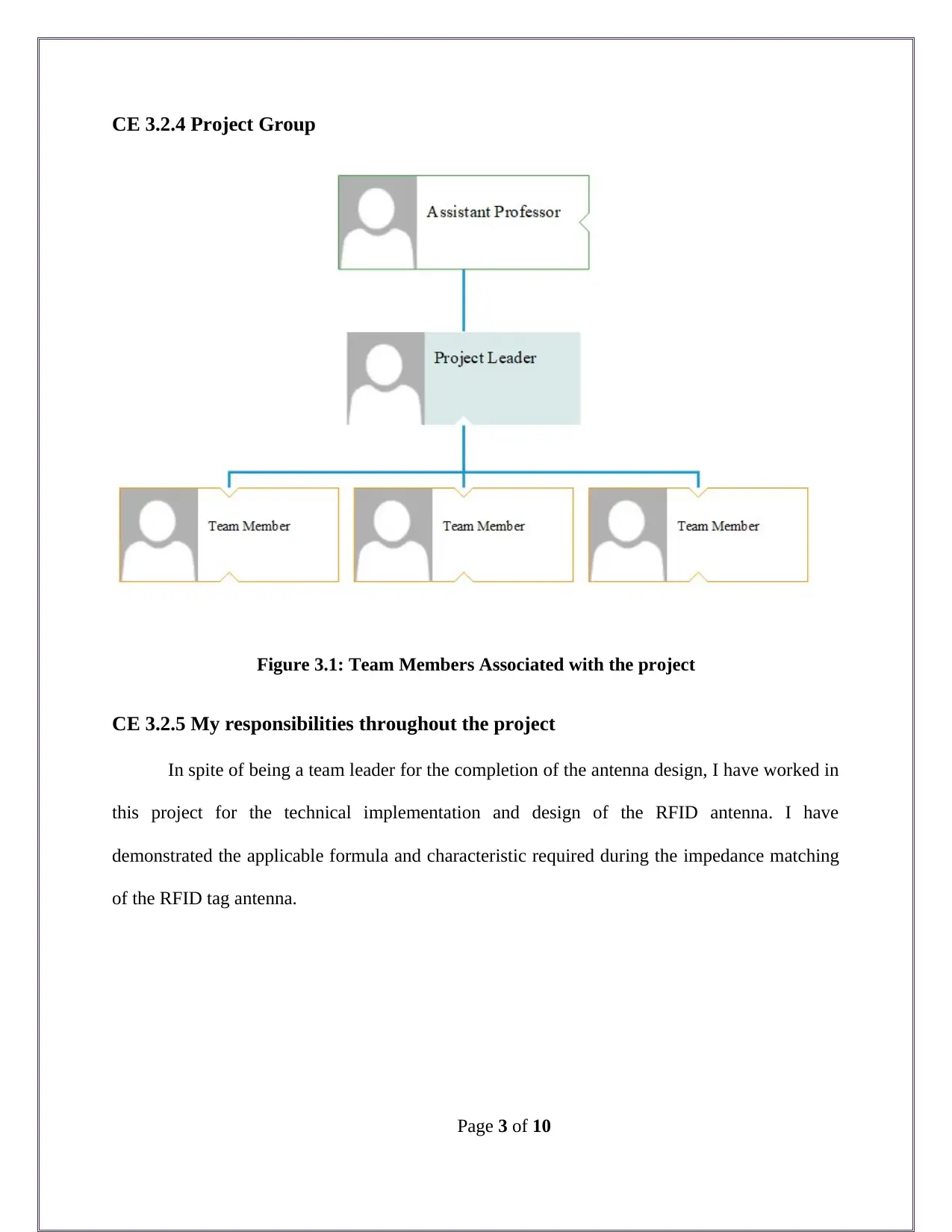
CE 3.2.4 Project Group
Figure 3.1: Team Members Associated with the project
CE 3.2.5 My responsibilities throughout the project
In spite of being a team leader for the completion of the antenna design, I have worked in
this project for the technical implementation and design of the RFID antenna. I have
demonstrated the applicable formula and characteristic required during the impedance matching
of the RFID tag antenna.
Page 3 of 10
Paraphrase This Document
Need a fresh take? Get an instant paraphrase of this document with our AI Paraphraser

CE 3.3 Distinctive Activity
CE 3.3.1 Comprehending the theory of the project
In this project, I have aimed at evaluating the technology and concept of RFID system
and antenna. I have introduces Friis formula while developing the required module of RFID
antenna. I have further developed the coefficient of power reflection formula while determining
the variation of the chip impedance. I have utilized a network analyzer for measuring the
variance of the chip impendence. I have considered the frequency and determined the variance in
respect to the change in the frequency level. I have used Avery Dennison AD-220 commercial
tag in this project with the application of HFSS software simulation package. In addition to that,
I have simulated the S parameter with customized Matlab codes. I have further calculated the
maximum theoretical read range of the antenna and compared the data with the results obtained
from this project. I have further verified the reflection coefficient with the simulation process
while matching with the impedance.
Figure 3.2: Working Principle of RFID System
Page 4 of 10

CE 3.3.2 Engineering knowledge and skills applied in the project
In this project, I have used the RF antenna and system for establishing the impedance
matching. I have represented the power density of the antenna at an R distance range by the
following formula:
W trans = [P trans G trans (θ trans, φ trans)] / 4 πR2
In the above equation, I have used (θ trans, φ trans) for indicating the direction of the
antenna, G trans as the reader antenna gain and P trans as the transmitting antenna power. I have
ensured that the value of represents the isotropic radiated power of the transmitter antenna.
Furthermore, for establishing the backward communication, I have used signal backscattering
process. In the measurement chamber of the RFID I have developed a monostatic setup. For
determining the matching complex of the reflection coefficient, I have determined the chip
impedance as the following:
Γ = ( Zc – Za ) / ( Zc + Za )
In the above equation, I have used Za for indicating the antenna resistance with
impedance and Zc as the impedance of the microchip. On the other hand, Γ is the coefficient of
power reflection. During the development and design of the antenna, I have ensured that the
value of Γ is always lesser than 1.
Page 5 of 10
⊘ This is a preview!⊘
Do you want full access?
Subscribe today to unlock all pages.

Trusted by 1+ million students worldwide
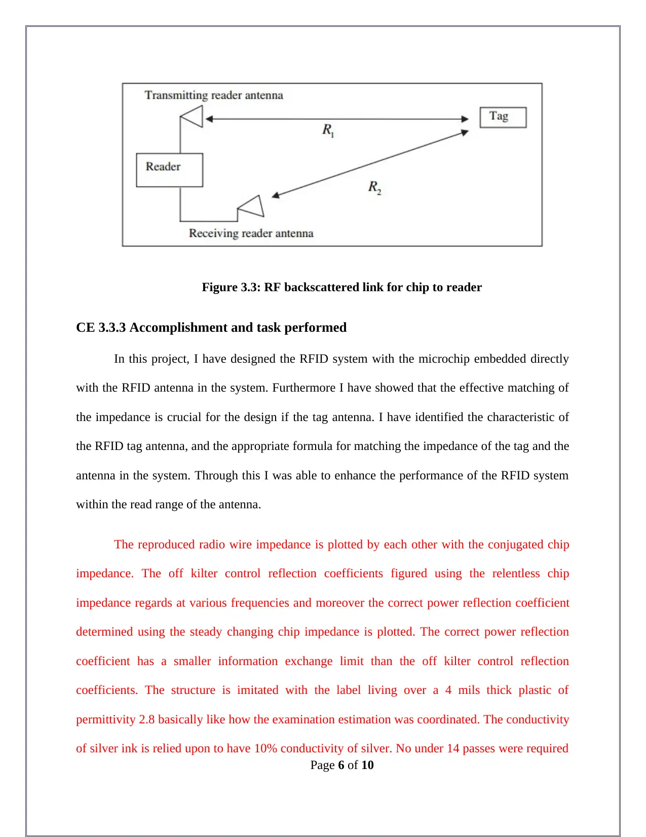
Figure 3.3: RF backscattered link for chip to reader
CE 3.3.3 Accomplishment and task performed
In this project, I have designed the RFID system with the microchip embedded directly
with the RFID antenna in the system. Furthermore I have showed that the effective matching of
the impedance is crucial for the design if the tag antenna. I have identified the characteristic of
the RFID tag antenna, and the appropriate formula for matching the impedance of the tag and the
antenna in the system. Through this I was able to enhance the performance of the RFID system
within the read range of the antenna.
The reproduced radio wire impedance is plotted by each other with the conjugated chip
impedance. The off kilter control reflection coefficients figured using the relentless chip
impedance regards at various frequencies and moreover the correct power reflection coefficient
determined using the steady changing chip impedance is plotted. The correct power reflection
coefficient has a smaller information exchange limit than the off kilter control reflection
coefficients. The structure is imitated with the label living over a 4 mils thick plastic of
permittivity 2.8 basically like how the examination estimation was coordinated. The conductivity
of silver ink is relied upon to have 10% conductivity of silver. No under 14 passes were required
Page 6 of 10
Paraphrase This Document
Need a fresh take? Get an instant paraphrase of this document with our AI Paraphraser

for the non-existent bit of the radio wire impedance to center to 0.5 degrees in this re-
authorization. Execution estimation of the tag was driven in the RFID anechoic chamber at The
University of Mississippi using the Voyantic Tagformance Lite RFID estimation system.
CE 3.3.4 Identified issues and their solutions
Issue: For developing the RFID system, I have designed the monostrip antenna. I have
focused on determining the maximum read range of the antenna through the developed RFID
setup. In the initial set of the system, I have ensured that the read range of the antenna is less than
the maximum distance that can be obtained with the backward and forward communication. I
have faced issue in the project when I found that the antenna failed to reflect the optimum power
that would be detected by the RFID tag.
Solution: For resolving the issue, I have turn the sensitivity of the receiving tag between
– 90 dBm to -70 dBm. In addition to that, I have kept the power of the threshold to -10 dBm.
Through this, I was able to achieve proper matching of the impedance property of the antenna.
Further, I was able to achieve accurate measurement of the read distance of the RFID antenna
used in the system.
CE 3.3.5 Plan to produce creative and innovative work
With the aim of providing innovative and creative work in this project, I have conducted
the analysis of the developed antenna using HPSS analysis software. I have conjugated the
antenna with the minimum impedance of the power chip foe maximizing the range of the read
power. During the implementation of the antenna design I have measured – 6 dBm of chip
impedance and – 11 dBm of operating power of the RFID chip. Further, I have included the
nonlinear extrapolation of the RFID while ensuring the −11 dBm of operating level during all the
Page 7 of 10

operational frequencies. Therefore, through HPSS analysis I was able to determine the impact of
the change in the impedance upon the performance of the antenna system.
CE 3.3.6 Collaborative work
I have focused on working as a team during the implementation of RFID system. I have
been working as a team leader for the successful completion of the project. I have identified the
work module and allocated effective team members for the timely completion of the design and
implementation. I have guided the team members with appropriate technical information and
practical knowledge that assisted in the project delivery within time and ensuring proper
standard.
CE 3.4 Project Review
CE 3.4.1 Project Overview
After completion of the project I was able to enhance the maximum reading range of the
RFID tag and dinner. With the application of backscattering theory I was able to maximize the
rate range while match the antenna impedance. The application of HFSS software has allowed
me to provide detailed analysis and standard of antenna testing. Moreover through this project I
was successful in providing guidelines for designing enhanced RFID antenna PDF
CE 3.4.2 My contribution to work
Throughout the project I have developed the plan for carrying out the implementation and
simulation of the RFID antenna. During the implementation process I have demonstrated my
skill in managing the project and applying technical information subsequently. Furthermore I
Page 8 of 10
⊘ This is a preview!⊘
Do you want full access?
Subscribe today to unlock all pages.

Trusted by 1+ million students worldwide

have looked over the work that were being conducted and directed the team members with any
Technical difficulties faced during the project.
Page 9 of 10
Technical difficulties faced during the project.
Page 9 of 10
1 out of 10
Related Documents
Your All-in-One AI-Powered Toolkit for Academic Success.
+13062052269
info@desklib.com
Available 24*7 on WhatsApp / Email
![[object Object]](/_next/static/media/star-bottom.7253800d.svg)
Unlock your academic potential
Copyright © 2020–2025 A2Z Services. All Rights Reserved. Developed and managed by ZUCOL.


