Comparative Analysis of TTL and CMOS Logic Families in Digital Design
VerifiedAdded on 2023/04/21
|5
|883
|396
Report
AI Summary
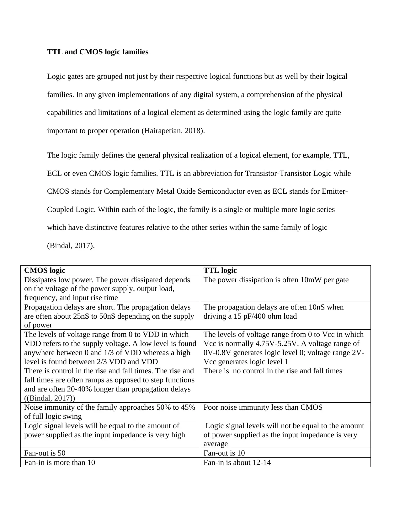
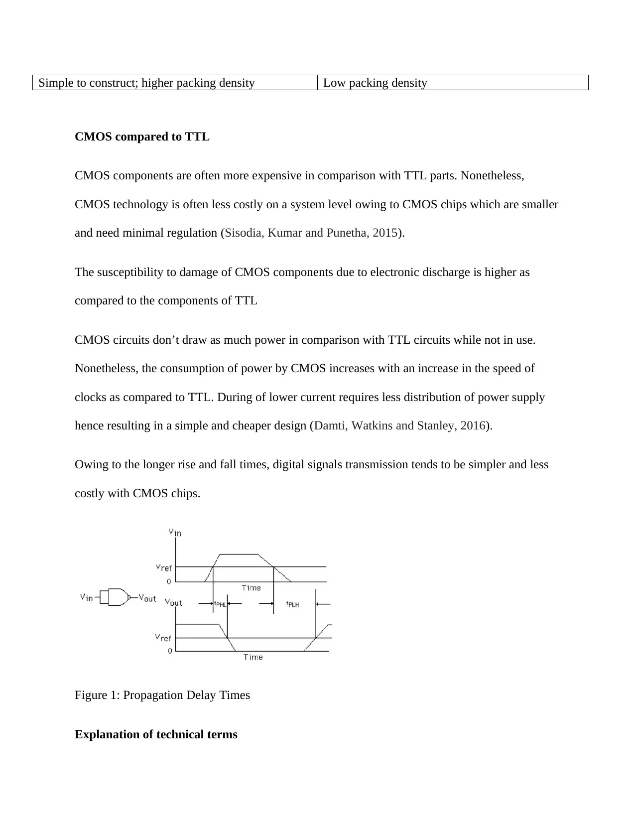
This report provides a comparative analysis of TTL (Transistor-Transistor Logic) and CMOS (Complementary Metal Oxide Semiconductor) logic families, essential components in digital system design. It explores the fundamental characteristics of each family, including power dissipation, propagation delays, voltage levels, noise immunity, fan-in, and fan-out. The report highlights the advantages and disadvantages of each logic family, such as CMOS's low power consumption and TTL's higher packing density, and discusses their respective applications. Technical terms like fan-in, fan-out, and noise immunity are clearly defined, providing a comprehensive understanding of the subject matter. References to relevant research and publications are included, offering further insights into the topic. This report serves as a valuable resource for students and professionals seeking to understand and compare these two core logic families in digital electronics.
1 out of 5

Your All-in-One AI-Powered Toolkit for Academic Success.
+13062052269
info@desklib.com
Available 24*7 on WhatsApp / Email
![[object Object]](/_next/static/media/star-bottom.7253800d.svg)
Copyright © 2020–2026 A2Z Services. All Rights Reserved. Developed and managed by ZUCOL.