Assignment on Inverting Amplifier Circuit
VerifiedAdded on 2020/04/15
|17
|1752
|41
AI Summary
Contribute Materials
Your contribution can guide someone’s learning journey. Share your
documents today.

0
Electronics 2
user
Electronics 2
user
Secure Best Marks with AI Grader
Need help grading? Try our AI Grader for instant feedback on your assignments.
Introduction
To increase the frequency response which an op-amp can be connected using negative feedback
to stabilize the gain. A small noise voltage can causes the extremely high open loop gain in an
unstable situation. Unwanted oscillation can also occur. In open loop gain parameter can vary
from one device to the next device. To creating an effective reduction gain, negative feedback is
back out of phase with the input. This closed loop gain is usually less than the open loop gain.
Op amp amplifier is basically divided into two types.
They are 1. Inverting OP-AMP Amplifier
2. Non-Inverting OP-AMP Amplifier
Non-inverting Operational Amplifier
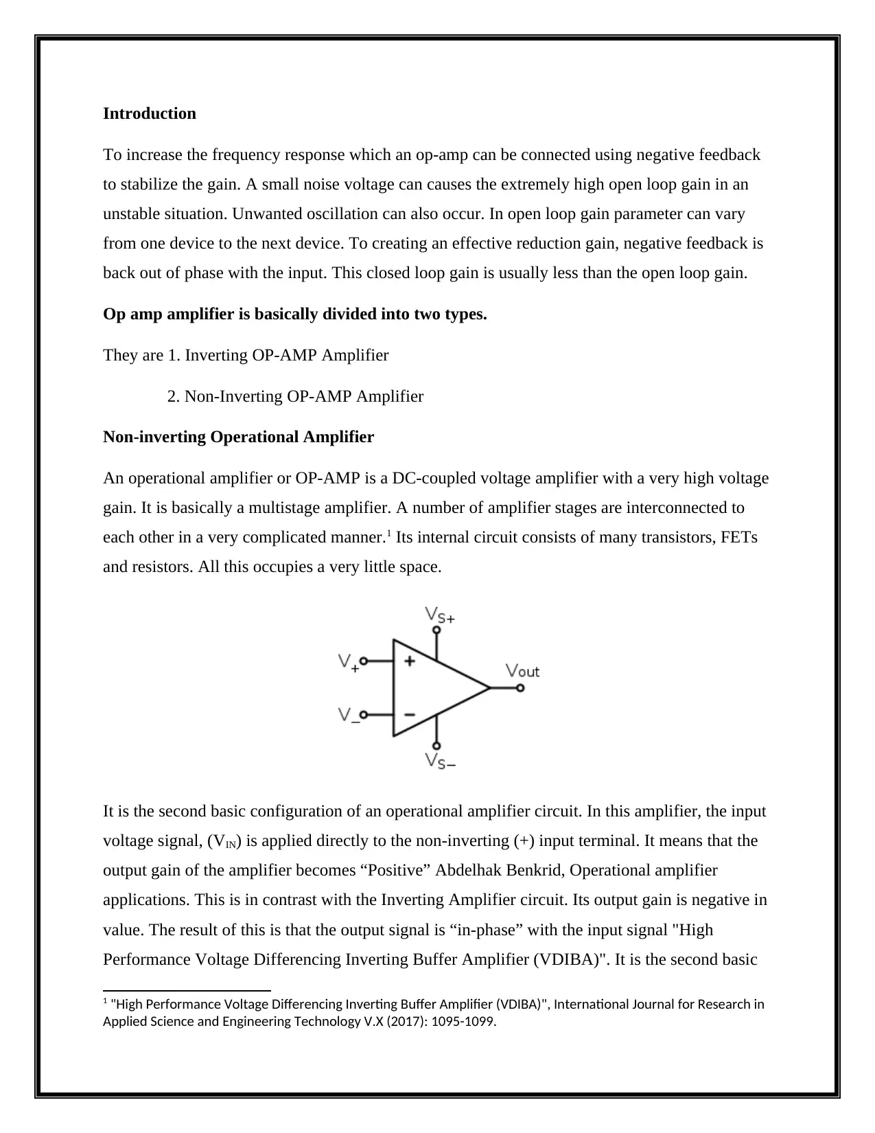
An operational amplifier or OP-AMP is a DC-coupled voltage amplifier with a very high voltage
gain. It is basically a multistage amplifier. A number of amplifier stages are interconnected to
each other in a very complicated manner.1 Its internal circuit consists of many transistors, FETs
and resistors. All this occupies a very little space.
It is the second basic configuration of an operational amplifier circuit. In this amplifier, the input
voltage signal, (VIN) is applied directly to the non-inverting (+) input terminal. It means that the
output gain of the amplifier becomes “Positive” Abdelhak Benkrid, Operational amplifier
applications. This is in contrast with the Inverting Amplifier circuit. Its output gain is negative in
value. The result of this is that the output signal is “in-phase” with the input signal "High
Performance Voltage Differencing Inverting Buffer Amplifier (VDIBA)". It is the second basic
1 "High Performance Voltage Differencing Inverting Buffer Amplifier (VDIBA)", International Journal for Research in
Applied Science and Engineering Technology V.X (2017): 1095-1099.
To increase the frequency response which an op-amp can be connected using negative feedback
to stabilize the gain. A small noise voltage can causes the extremely high open loop gain in an
unstable situation. Unwanted oscillation can also occur. In open loop gain parameter can vary
from one device to the next device. To creating an effective reduction gain, negative feedback is
back out of phase with the input. This closed loop gain is usually less than the open loop gain.
Op amp amplifier is basically divided into two types.
They are 1. Inverting OP-AMP Amplifier
2. Non-Inverting OP-AMP Amplifier
Non-inverting Operational Amplifier
An operational amplifier or OP-AMP is a DC-coupled voltage amplifier with a very high voltage
gain. It is basically a multistage amplifier. A number of amplifier stages are interconnected to
each other in a very complicated manner.1 Its internal circuit consists of many transistors, FETs
and resistors. All this occupies a very little space.
It is the second basic configuration of an operational amplifier circuit. In this amplifier, the input
voltage signal, (VIN) is applied directly to the non-inverting (+) input terminal. It means that the
output gain of the amplifier becomes “Positive” Abdelhak Benkrid, Operational amplifier
applications. This is in contrast with the Inverting Amplifier circuit. Its output gain is negative in
value. The result of this is that the output signal is “in-phase” with the input signal "High
Performance Voltage Differencing Inverting Buffer Amplifier (VDIBA)". It is the second basic
1 "High Performance Voltage Differencing Inverting Buffer Amplifier (VDIBA)", International Journal for Research in
Applied Science and Engineering Technology V.X (2017): 1095-1099.
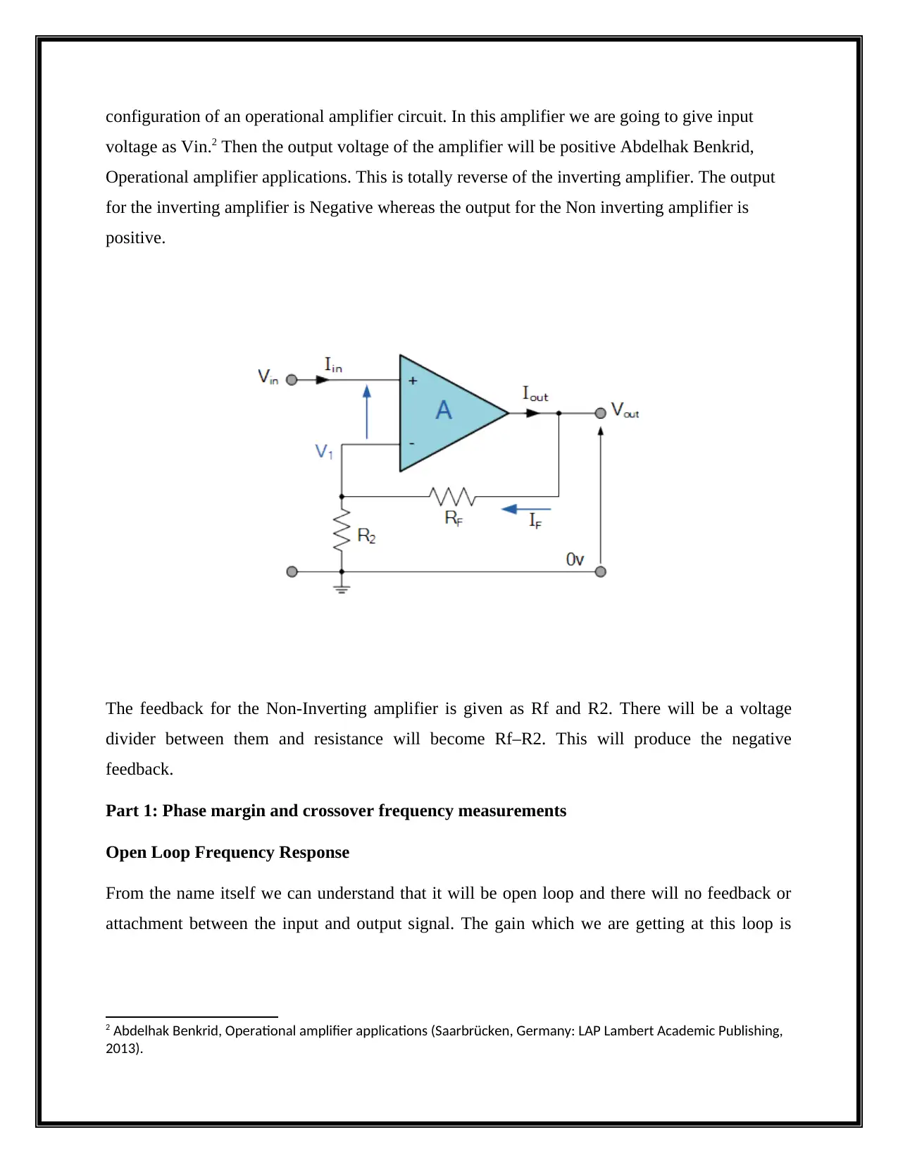
configuration of an operational amplifier circuit. In this amplifier we are going to give input
voltage as Vin.2 Then the output voltage of the amplifier will be positive Abdelhak Benkrid,
Operational amplifier applications. This is totally reverse of the inverting amplifier. The output
for the inverting amplifier is Negative whereas the output for the Non inverting amplifier is
positive.
The feedback for the Non-Inverting amplifier is given as Rf and R2. There will be a voltage
divider between them and resistance will become Rf–R2. This will produce the negative
feedback.
Part 1: Phase margin and crossover frequency measurements
Open Loop Frequency Response
From the name itself we can understand that it will be open loop and there will no feedback or
attachment between the input and output signal. The gain which we are getting at this loop is
2 Abdelhak Benkrid, Operational amplifier applications (Saarbrücken, Germany: LAP Lambert Academic Publishing,
2013).
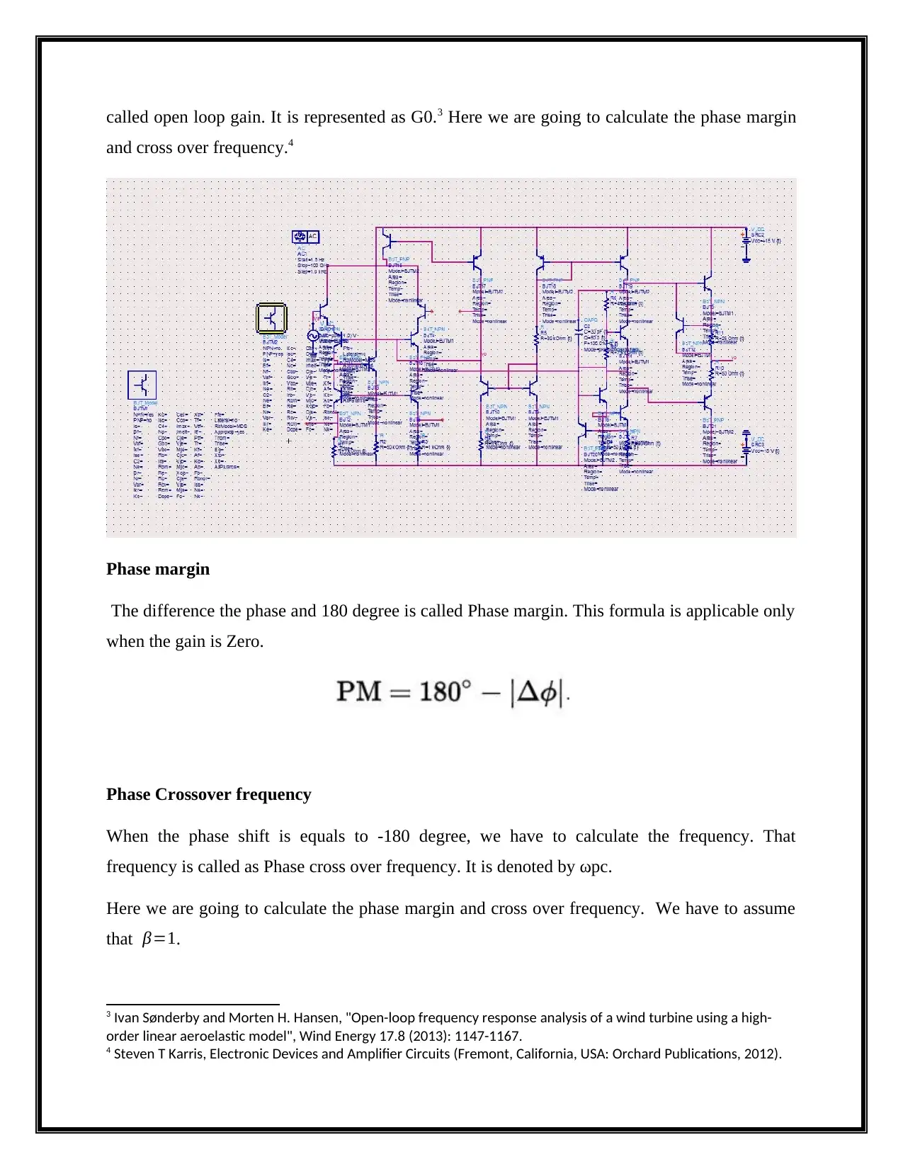
called open loop gain. It is represented as G0.3 Here we are going to calculate the phase margin
and cross over frequency.4
Phase margin
The difference the phase and 180 degree is called Phase margin. This formula is applicable only
when the gain is Zero.
Phase Crossover frequency
When the phase shift is equals to -180 degree, we have to calculate the frequency. That
frequency is called as Phase cross over frequency. It is denoted by ωpc.
Here we are going to calculate the phase margin and cross over frequency. We have to assume
that β=1.
3 Ivan Sønderby and Morten H. Hansen, "Open-loop frequency response analysis of a wind turbine using a high-
order linear aeroelastic model", Wind Energy 17.8 (2013): 1147-1167.
4 Steven T Karris, Electronic Devices and Amplifier Circuits (Fremont, California, USA: Orchard Publications, 2012).
Secure Best Marks with AI Grader
Need help grading? Try our AI Grader for instant feedback on your assignments.
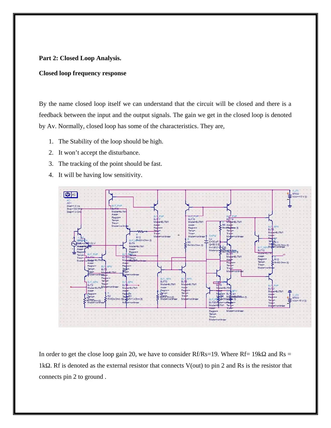
Part 2: Closed Loop Analysis.
Closed loop frequency response
By the name closed loop itself we can understand that the circuit will be closed and there is a
feedback between the input and the output signals. The gain we get in the closed loop is denoted
by Av. Normally, closed loop has some of the characteristics. They are,
1. The Stability of the loop should be high.
2. It won’t accept the disturbance.
3. The tracking of the point should be fast.
4. It will be having low sensitivity.
In order to get the close loop gain 20, we have to consider Rf/Rs=19. Where Rf= 19kΩ and Rs =
1kΩ. Rf is denoted as the external resistor that connects V(out) to pin 2 and Rs is the resistor that
connects pin 2 to ground .
Question 3:
Dominant Pole Compensation
The Dominant pole compensation can be find very easily. Simply take the pole which is the
lowest. This pole should not dominant among other poles. This pole should be having low
frequency among other poles.5 It is very effective method to implement the dominant pole. It will
helps the following characteristics to improve.6 They are
1. It helps to reduce the bandwidth7
2. It will increases the phase margin which is present in the crossover frequency.
3. By using the bandwidth, the magnitude of T will be reduced.
Parts 3, 4, 5 and 6 Dominant Pole Compensation
Compensation Capacitor Determination
Normally the compensation will be doing to get the stable operation. There are so many types of
compensation. But here we are using Miller compensation.8 In Miller compensation we are going
to compensate the capacitor.9 With the help of the Miller Capacitor, The forward path will be
blocked by compensating capacitor. The RHP will be eliminated to zero.10
5 Carey Witkov, Nonlinear resonance, 2011.
6 Seunggyun Cheong and Robert R. Bitmead, "Divination of closed-loop stability and performance via frequency
response function estimates", Automatica 48.7 (2012): 1405-1414.
7 Wolfgang Hofmann, J Schlabbach and Wolfgang Just, Reactive power compensation (Chichester, West Sussex,
U.K.: Wiley, 2012).
8 Zhao Li, Multipath Miller compensation for switched-capacitor systems (Waterloo, Ont.: University of Waterloo,
2011).
9 Hoe-Kyung Jung, Future information communication technology and applications (Dordrecht: Springer, 2013).
10 Yi Fan Zeng and Fang Fang Jiang, "Error Compensation for Single Pair-Pole Encoder Based on Ellipse Hypothesis",
Advanced Materials Research 591-593 (2012): 1231-1235.
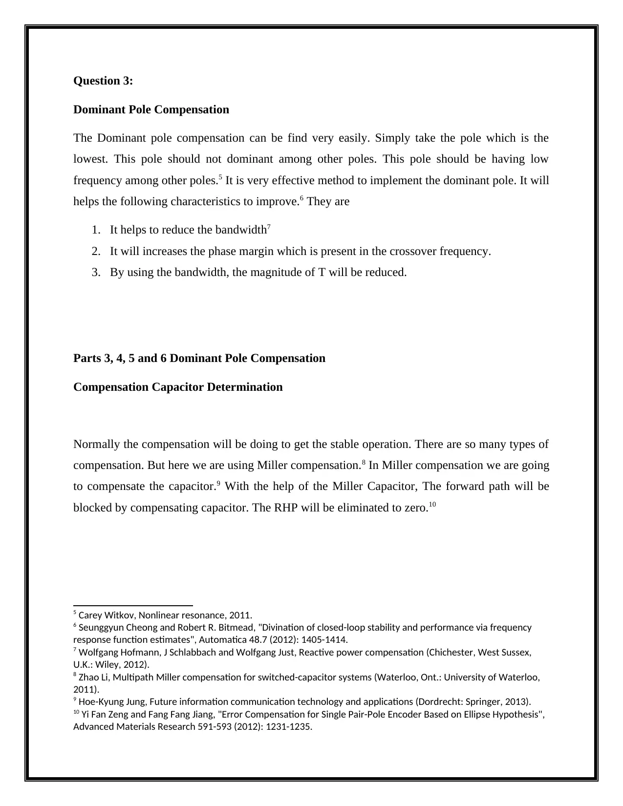
Emitter follower is also called as common collector. It is one of the single stage bipolar junction
transistor. It is used as a voltage buffer. In this circuit, base terminal is input, emitter will be the
output and the collector is the common.
Gain Ratio = 110/19 =5.789
Cp = 1/2πRfp
fp = Cp*2*π*R= 30p*2*π*19k = 357 μHz
fp=fcnew/(110/19) =
fcnew=fp*5.789= 20.6mHZ
fcnew = 0.1*fh = 2.06 Hz
transistor. It is used as a voltage buffer. In this circuit, base terminal is input, emitter will be the
output and the collector is the common.
Gain Ratio = 110/19 =5.789
Cp = 1/2πRfp
fp = Cp*2*π*R= 30p*2*π*19k = 357 μHz
fp=fcnew/(110/19) =
fcnew=fp*5.789= 20.6mHZ
fcnew = 0.1*fh = 2.06 Hz
Paraphrase This Document
Need a fresh take? Get an instant paraphrase of this document with our AI Paraphraser
fcnew = 0.2*fh = 4.12hz
fcnew = 0.3*fh = 6.18hz
fcnew = 0.4*fh = 8.24hz
fcnew = 0.5*fh = 10.3hz
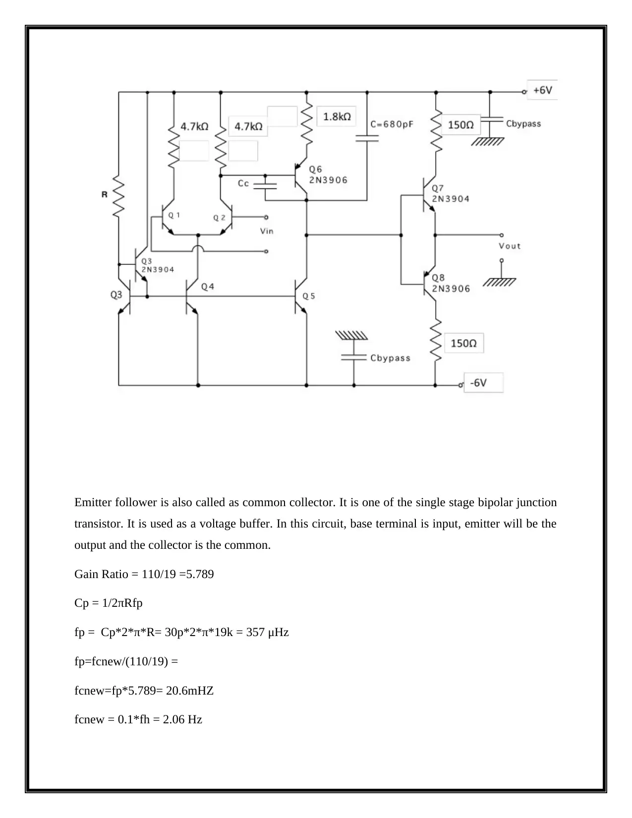
Question 5:
Compensation Capacitor Implementation
Implement the compensation and measure the actual compensated crossover frequency and phase margin
(using the schematic of part 1, the one with the loading of the feedback).Measure the new crossover
frequency and phase margin. Is it close to your design?
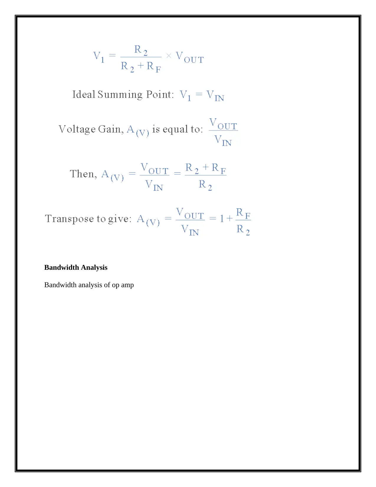
The Frequecy response ia analysed by plotting the graph between the gain and the frequency.It s
used to study about the change in the gain with respect to the frequency. 11 The respresentation of
the graph is known as Bode Plot.This plot shows the variation in the frequency with respect to
the gain .It displays a band of frequency which have constant gain is known as bandwidth. 12
11 Namika Kumari, "Design and Analysis of Two-Stage Operational Transconductance Amplifier with Compensation
Capacitor", Engineering and Technology Journal (2017)
12 Jinliang GONG, "Closed Loop Design Method of Micro-driving Displacement Amplifier Module Targeting for
Stiffness", Journal of Mechanical Engineering 48.15 (2012): 58.
fcnew = 0.3*fh = 6.18hz
fcnew = 0.4*fh = 8.24hz
fcnew = 0.5*fh = 10.3hz
Question 5:
Compensation Capacitor Implementation
Implement the compensation and measure the actual compensated crossover frequency and phase margin
(using the schematic of part 1, the one with the loading of the feedback).Measure the new crossover
frequency and phase margin. Is it close to your design?
The Frequecy response ia analysed by plotting the graph between the gain and the frequency.It s
used to study about the change in the gain with respect to the frequency. 11 The respresentation of
the graph is known as Bode Plot.This plot shows the variation in the frequency with respect to
the gain .It displays a band of frequency which have constant gain is known as bandwidth. 12
11 Namika Kumari, "Design and Analysis of Two-Stage Operational Transconductance Amplifier with Compensation
Capacitor", Engineering and Technology Journal (2017)
12 Jinliang GONG, "Closed Loop Design Method of Micro-driving Displacement Amplifier Module Targeting for
Stiffness", Journal of Mechanical Engineering 48.15 (2012): 58.
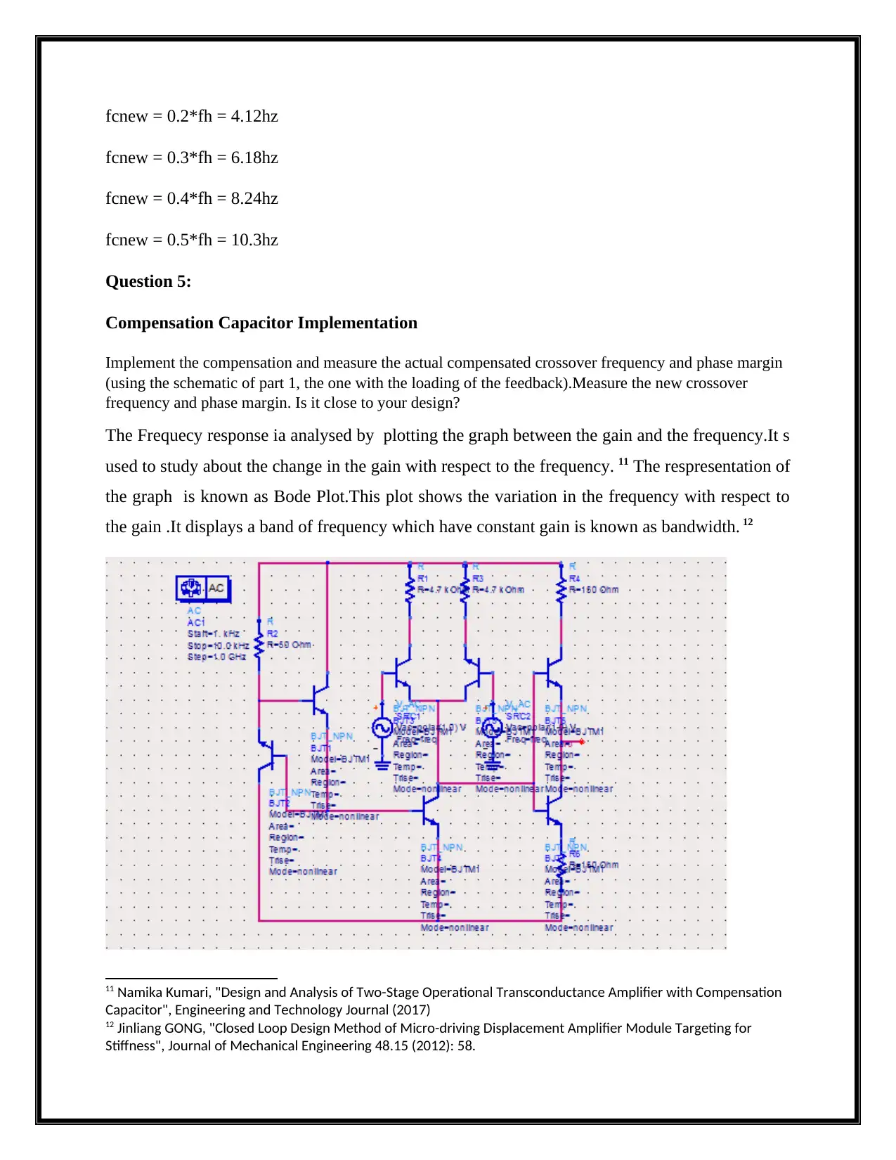
Frequency Response of Circuit:
The Output Power with Corner Frequencies can also be calculated by
The Output Power with Corner Frequencies can also be calculated by
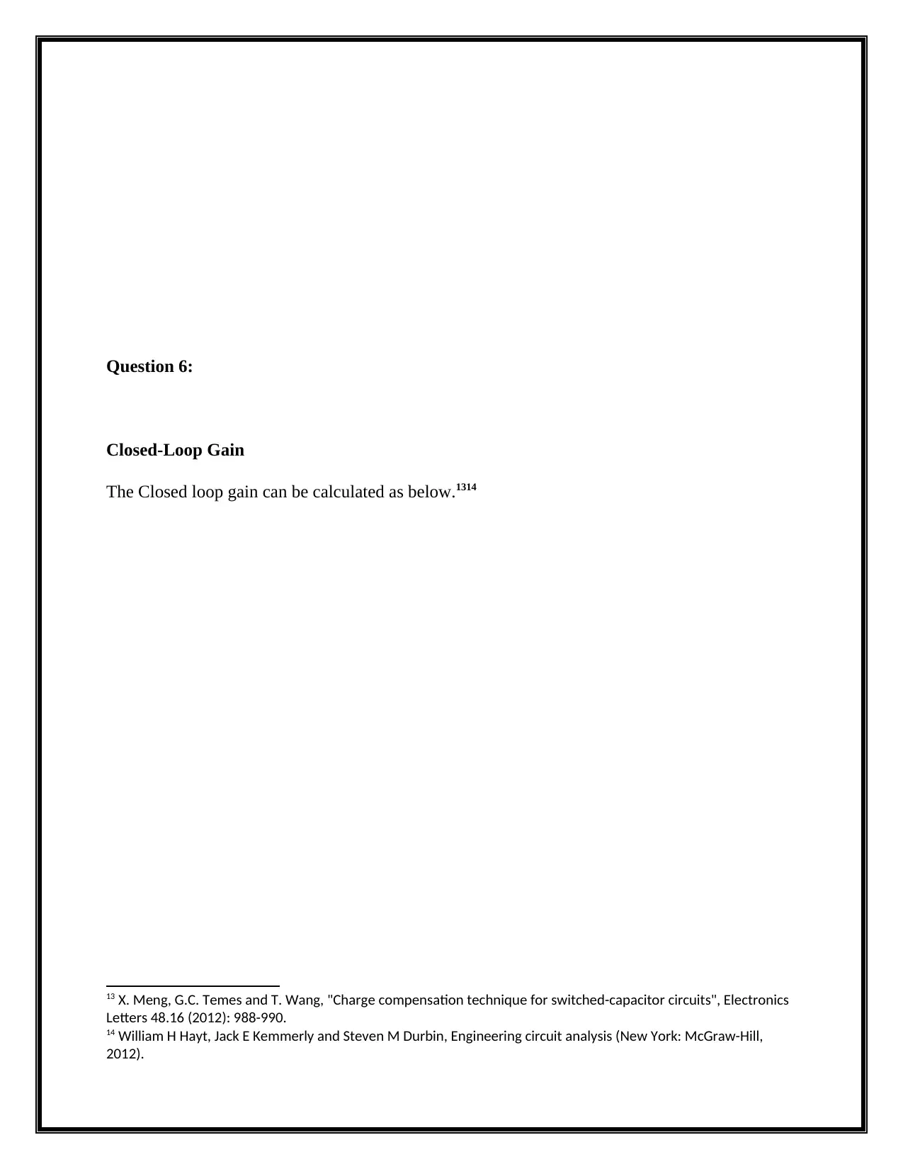
Question 6:
Closed-Loop Gain
The Closed loop gain can be calculated as below.1314
13 X. Meng, G.C. Temes and T. Wang, "Charge compensation technique for switched-capacitor circuits", Electronics
Letters 48.16 (2012): 988-990.
14 William H Hayt, Jack E Kemmerly and Steven M Durbin, Engineering circuit analysis (New York: McGraw-Hill,
2012).
Secure Best Marks with AI Grader
Need help grading? Try our AI Grader for instant feedback on your assignments.
Bandwidth Analysis
Bandwidth analysis of op amp
Bandwidth analysis of op amp
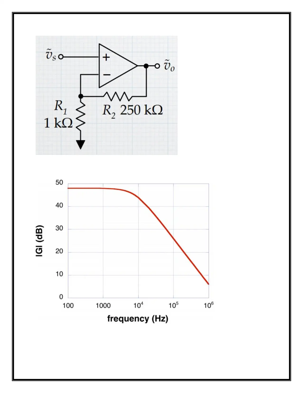
The op amp gain should have the low pass kind of the frequency dependence. 15 For improving
the amp stability, the capacitor is added in the circuit. 16 The closed-loop amp corner frequency
alter with a gain. The op-amp open-loop gain should have the low-pass kind of the behavior. 17
A → A ( S )= A0
1+ S
ωb
A0 - The gain at the very low frequency
ωbOpen-loop gain corner frequency
15 X. Meng, G.C. Temes and T. Wang, "Charge compensation technique for switched-capacitor circuits", Electronics
Letters 48.16 (2012): 988-990.
16 G. Giustolisi and G. Palumbo, "Compensation strategy for high-speed three-stage switched-capacitor amplifiers",
Electronics Letters 52.14 (2016): 1202-1204.
17 Kenneth Y Jo, Satellite communications network design and analysis (Boston: Artech House, 2011).
Paraphrase This Document
Need a fresh take? Get an instant paraphrase of this document with our AI Paraphraser
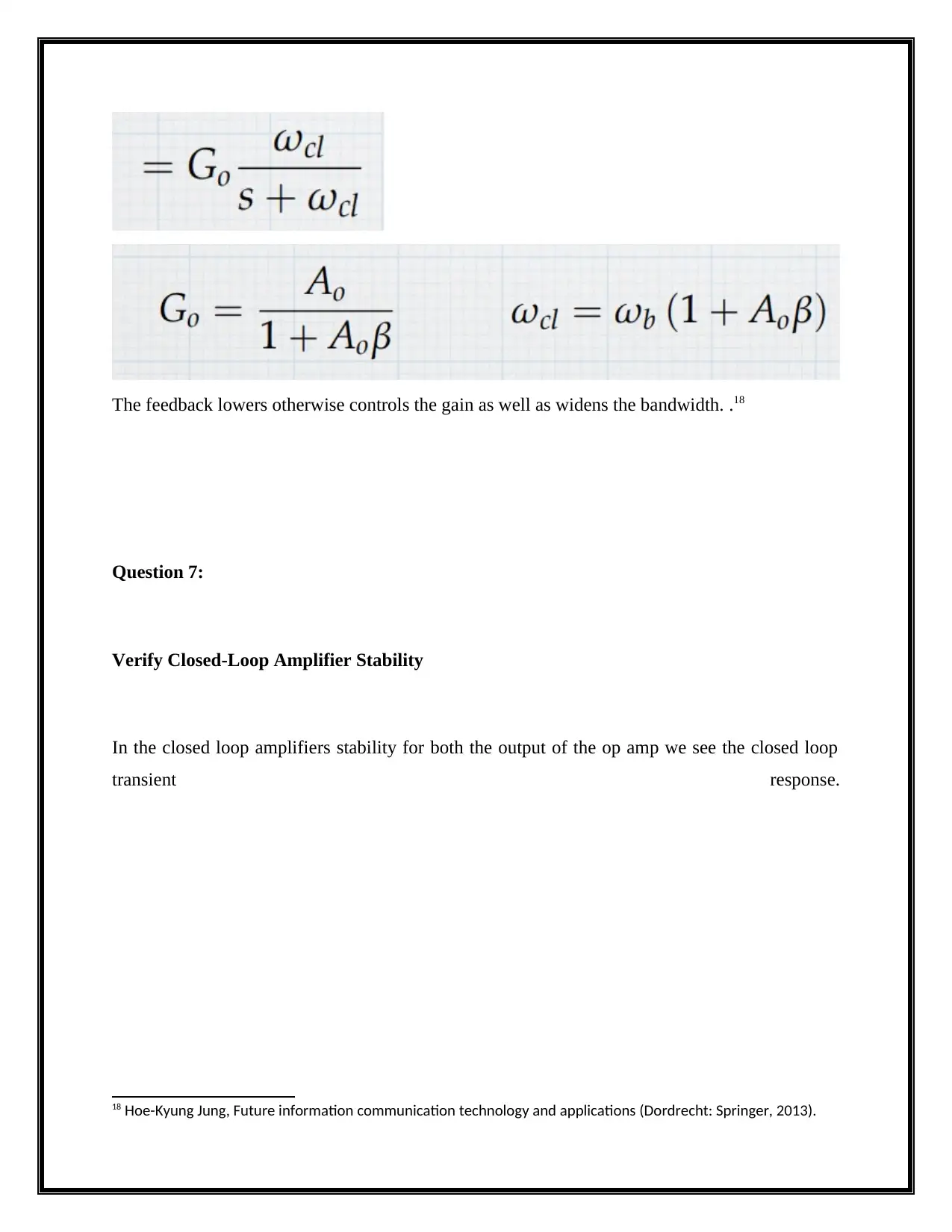
The feedback lowers otherwise controls the gain as well as widens the bandwidth. .18
Question 7:
Verify Closed-Loop Amplifier Stability
In the closed loop amplifiers stability for both the output of the op amp we see the closed loop
transient response.
18 Hoe-Kyung Jung, Future information communication technology and applications (Dordrecht: Springer, 2013).
Question 7:
Verify Closed-Loop Amplifier Stability
In the closed loop amplifiers stability for both the output of the op amp we see the closed loop
transient response.
18 Hoe-Kyung Jung, Future information communication technology and applications (Dordrecht: Springer, 2013).
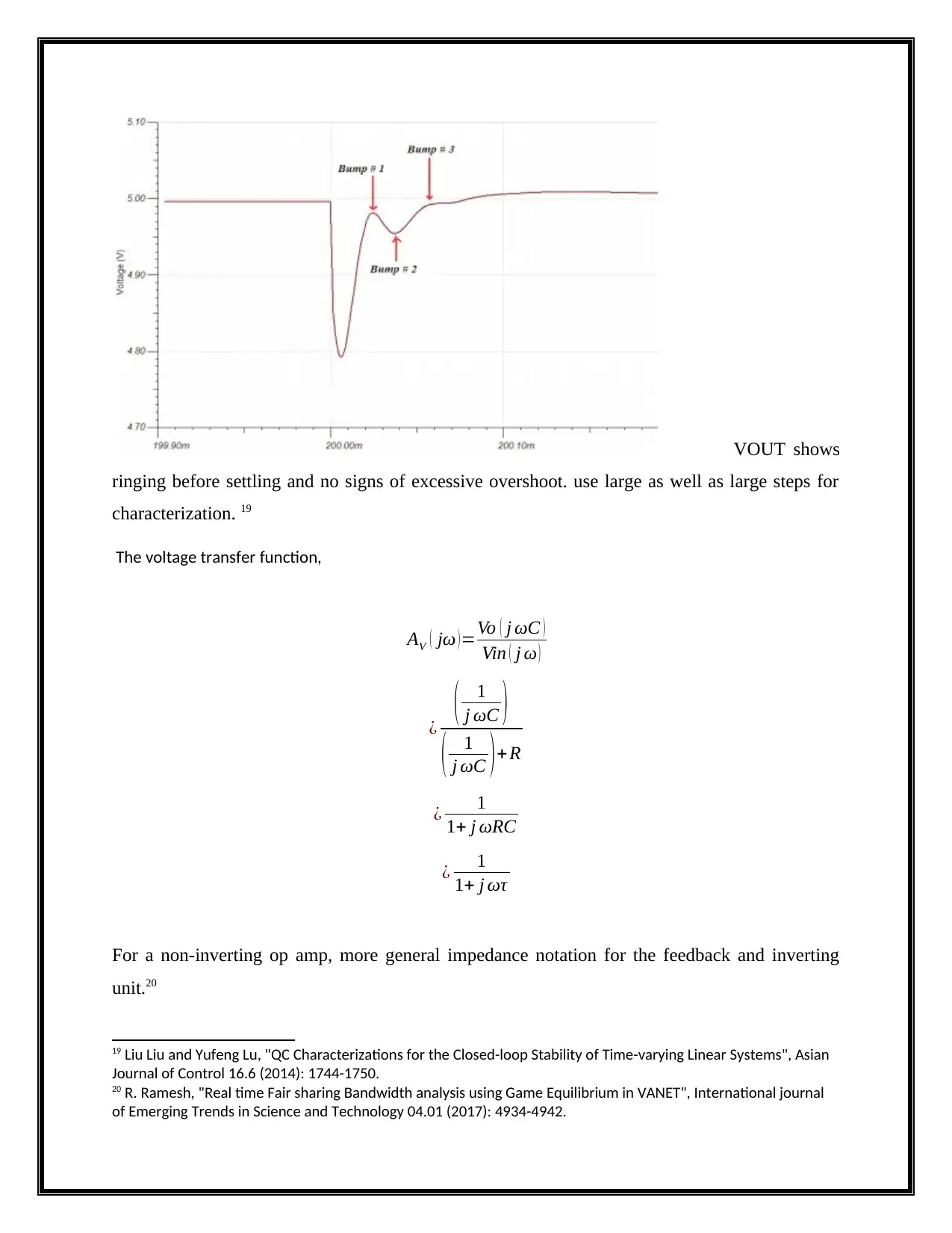
VOUT shows
ringing before settling and no signs of excessive overshoot. use large as well as large steps for
characterization. 19
The voltage transfer function,
AV ( jω )=Vo ( j ωC )
Vin ( j ω )
¿ ( 1
j ωC )
( 1
j ωC )+ R
¿ 1
1+ j ωRC
¿ 1
1+ j ωτ
For a non-inverting op amp, more general impedance notation for the feedback and inverting
unit.20
19 Liu Liu and Yufeng Lu, "QC Characterizations for the Closed-loop Stability of Time-varying Linear Systems", Asian
Journal of Control 16.6 (2014): 1744-1750.
20 R. Ramesh, "Real time Fair sharing Bandwidth analysis using Game Equilibrium in VANET", International journal
of Emerging Trends in Science and Technology 04.01 (2017): 4934-4942.
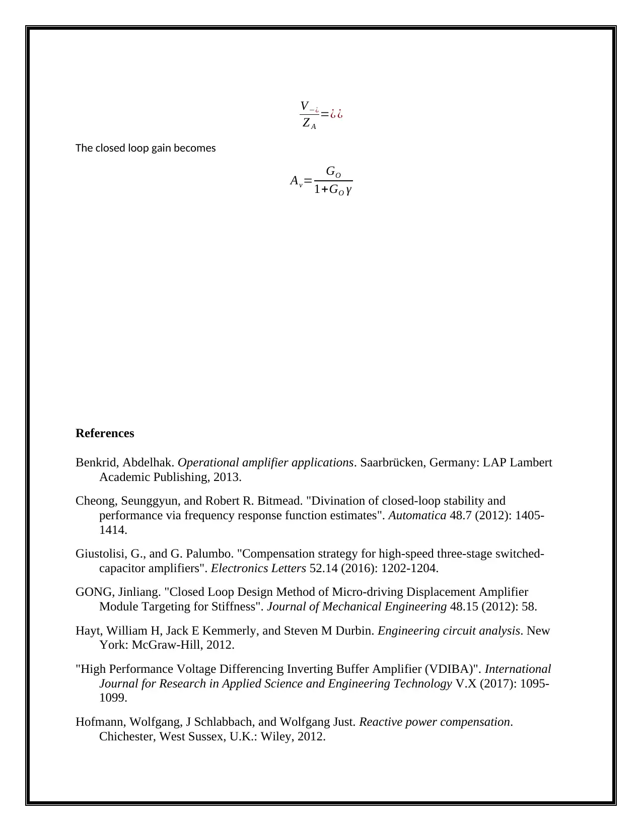
V−¿
Z A
=¿ ¿
The closed loop gain becomes
Av= GO
1+GO γ
References
Benkrid, Abdelhak. Operational amplifier applications. Saarbrücken, Germany: LAP Lambert
Academic Publishing, 2013.
Cheong, Seunggyun, and Robert R. Bitmead. "Divination of closed-loop stability and
performance via frequency response function estimates". Automatica 48.7 (2012): 1405-
1414.
Giustolisi, G., and G. Palumbo. "Compensation strategy for high-speed three-stage switched-
capacitor amplifiers". Electronics Letters 52.14 (2016): 1202-1204.
GONG, Jinliang. "Closed Loop Design Method of Micro-driving Displacement Amplifier
Module Targeting for Stiffness". Journal of Mechanical Engineering 48.15 (2012): 58.
Hayt, William H, Jack E Kemmerly, and Steven M Durbin. Engineering circuit analysis. New
York: McGraw-Hill, 2012.
"High Performance Voltage Differencing Inverting Buffer Amplifier (VDIBA)". International
Journal for Research in Applied Science and Engineering Technology V.X (2017): 1095-
1099.
Hofmann, Wolfgang, J Schlabbach, and Wolfgang Just. Reactive power compensation.
Chichester, West Sussex, U.K.: Wiley, 2012.
Secure Best Marks with AI Grader
Need help grading? Try our AI Grader for instant feedback on your assignments.
Jo, Kenneth Y. Satellite communications network design and analysis. Boston: Artech House,
2011.
Jung, Hoe-Kyung. Future information communication technology and applications. Dordrecht:
Springer, 2013.
Karris, Steven T. Electronic Devices and Amplifier Circuits. Fremont, California, USA: Orchard
Publications, 2012.
Kumari, Namika. "Design and Analysis of Two-Stage Operational Transconductance Amplifier
with Compensation Capacitor". Engineering and Technology Journal (2017).
Li, Zhao. Multipath Miller compensation for switched-capacitor systems. Waterloo, Ont.:
University of Waterloo, 2011.
Liu, Liu, and Yufeng Lu. "QC Characterizations for the Closed-loop Stability of Time-varying
Linear Systems". Asian Journal of Control 16.6 (2014): 1744-1750.
Meng, X., G.C. Temes, and T. Wang. "Charge compensation technique for switched-capacitor
circuits". Electronics Letters 48.16 (2012): 988-990.
Ramesh, R. "Real time Fair sharing Bandwidth analysis using Game Equilibrium in
VANET". International journal of Emerging Trends in Science and Technology 04.01
(2017): 4934-4942.
Sønderby, Ivan, and Morten H. Hansen. "Open-loop frequency response analysis of a wind
turbine using a high-order linear aeroelastic model". Wind Energy 17.8 (2013): 1147-1167.
Witkov, Carey. Nonlinear resonance, 2011.
Zeng, Yi Fan, and Fang Fang Jiang. "Error Compensation for Single Pair-Pole Encoder Based on
Ellipse Hypothesis". Advanced Materials Research 591-593 (2012): 1231-1235.
1 out of 17
Related Documents


Your All-in-One AI-Powered Toolkit for Academic Success.
+13062052269
info@desklib.com
Available 24*7 on WhatsApp / Email
![[object Object]](/_next/static/media/star-bottom.7253800d.svg)
Unlock your academic potential
© 2024 | Zucol Services PVT LTD | All rights reserved.