VLSI Techniques ELEC 30007: CMOS Transistor Based Half Adder Design
VerifiedAdded on 2023/06/12
|7
|763
|484
Homework Assignment
AI Summary
This assignment solution for VLSI Techniques (ELEC 30007) addresses two primary problems: calculating the resistance of a polysilicon wire and designing a half-adder circuit using CMOS transistors. The resistance calculation utilizes the sheet resistance value and the dimensions of the wire. The half-a...
VLSI Techniques-ELEC 30007 –SPRING-2018 – CW1–QP
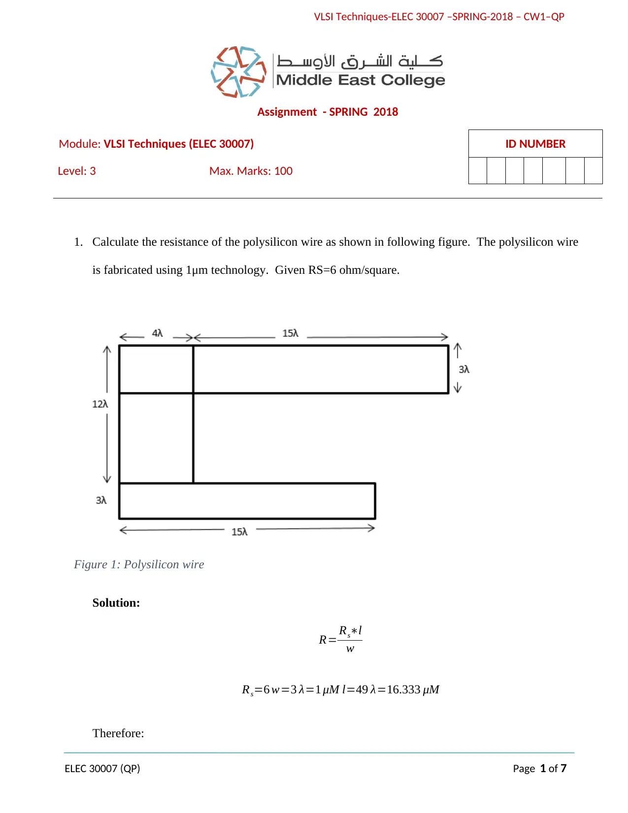
1. Calculate the resistance of the polysilicon wire as shown in following figure. The polysilicon wire
is fabricated using 1μm technology. Given RS=6 ohm/square.
Figure 1: Polysilicon wire
Solution:
R= Rs∗l
w
Rs=6 w=3 λ=1 μM l=49 λ=16.333 μM
Therefore:
ELEC 30007 (QP) Page 1 of 7
Assignment - SPRING 2018
Module: VLSI Techniques (ELEC 30007) ID NUMBER
Level: 3 Max. Marks: 100
Paraphrase This Document
Need a fresh take? Get an instant paraphrase of this document with our AI Paraphraser
VLSI Techniques-ELEC 30007 –SPRING-2018 – CW1–QP
R=6∗49
3∗1 =98 Ω
Resistance of the polysilicon wire=98 Ω
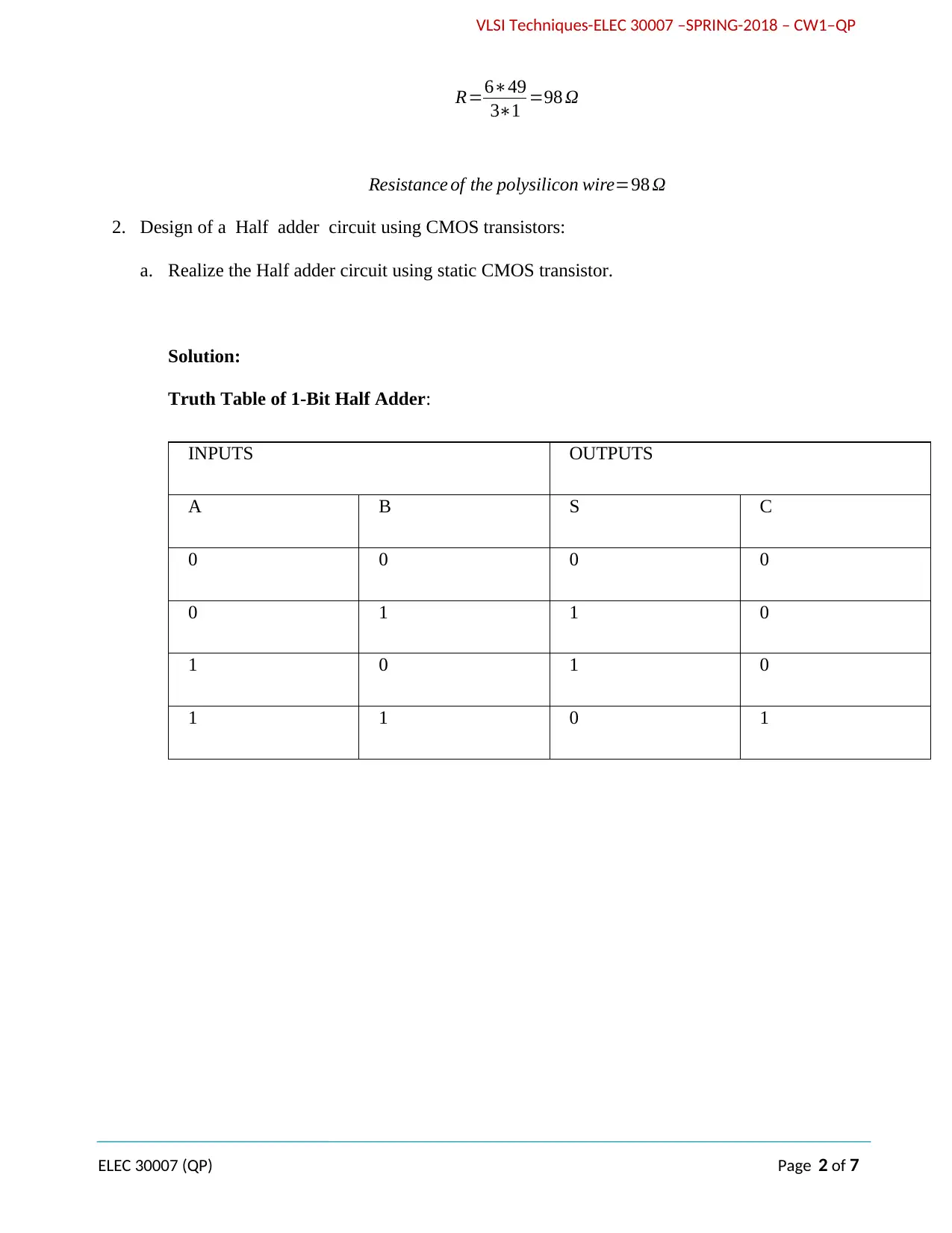
2. Design of a Half adder circuit using CMOS transistors:
a. Realize the Half adder circuit using static CMOS transistor.
Solution:
Truth Table of 1-Bit Half Adder:
INPUTS OUTPUTS
A B S C
0 0 0 0
0 1 1 0
1 0 1 0
1 1 0 1
ELEC 30007 (QP) Page 2 of 7
VLSI Techniques-ELEC 30007 –SPRING-2018 – CW1–QP
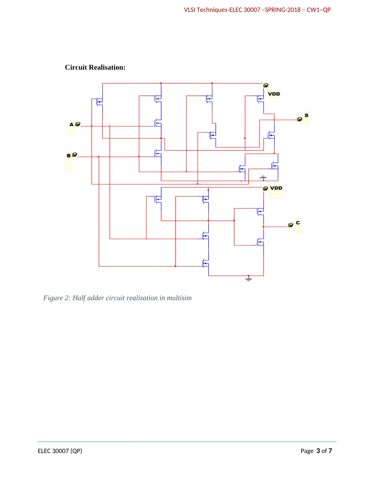
Circuit Realisation:
Figure 2: Half adder circuit realization in multisim
ELEC 30007 (QP) Page 3 of 7
Circuit Realisation:
Figure 2: Half adder circuit realization in multisim
ELEC 30007 (QP) Page 3 of 7
⊘ This is a preview!⊘
Do you want full access?
Subscribe today to unlock all pages.

Trusted by 1+ million students worldwide
VLSI Techniques-ELEC 30007 –SPRING-2018 – CW1–QP
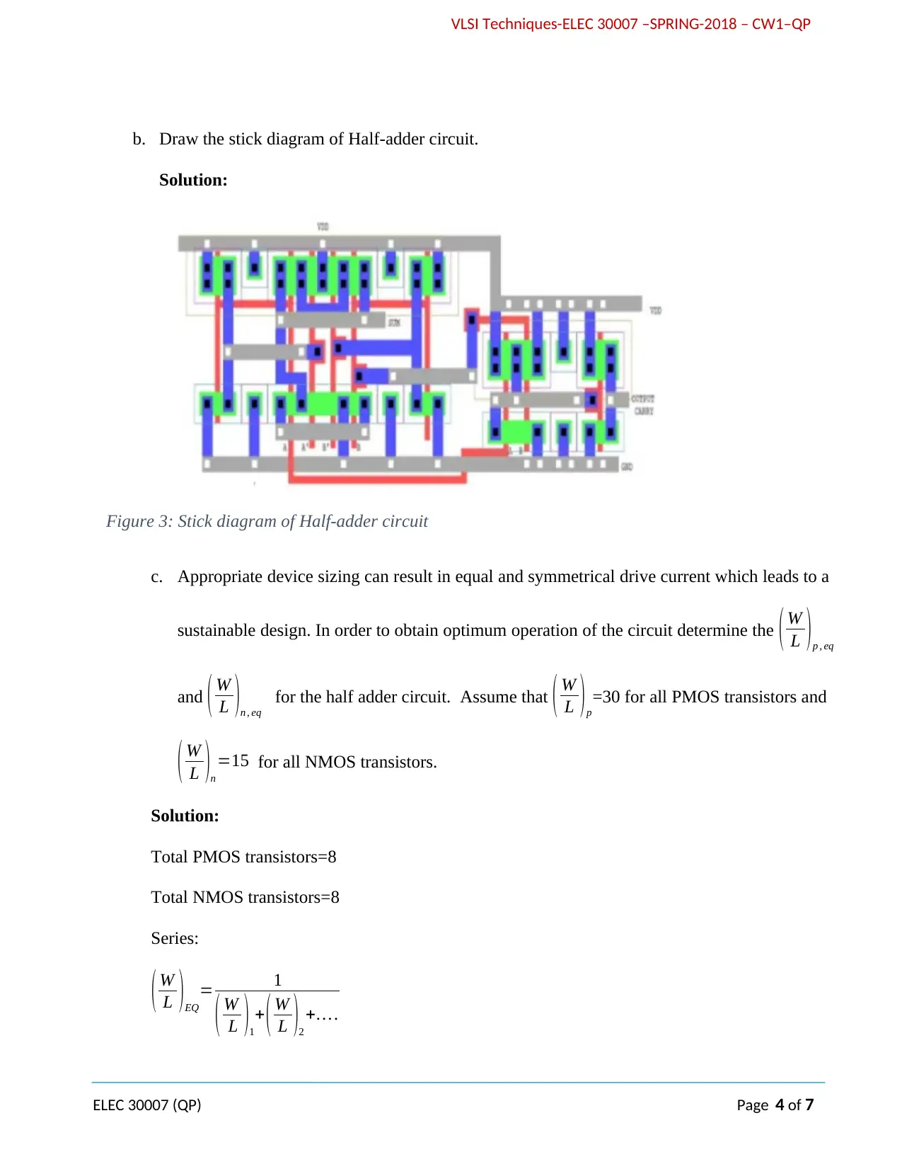
b. Draw the stick diagram of Half-adder circuit.
Solution:
Figure 3: Stick diagram of Half-adder circuit
c. Appropriate device sizing can result in equal and symmetrical drive current which leads to a
sustainable design. In order to obtain optimum operation of the circuit determine the ( W
L )p , eq
and ( W
L )n , eq
for the half adder circuit. Assume that ( W
L )p
=30 for all PMOS transistors and
( W
L )n
=15 for all NMOS transistors.
Solution:
Total PMOS transistors=8
Total NMOS transistors=8
Series:
( W
L ) EQ
= 1
( W
L )1
+ ( W
L )2
+… .
ELEC 30007 (QP) Page 4 of 7
Paraphrase This Document
Need a fresh take? Get an instant paraphrase of this document with our AI Paraphraser
VLSI Techniques-ELEC 30007 –SPRING-2018 – CW1–QP
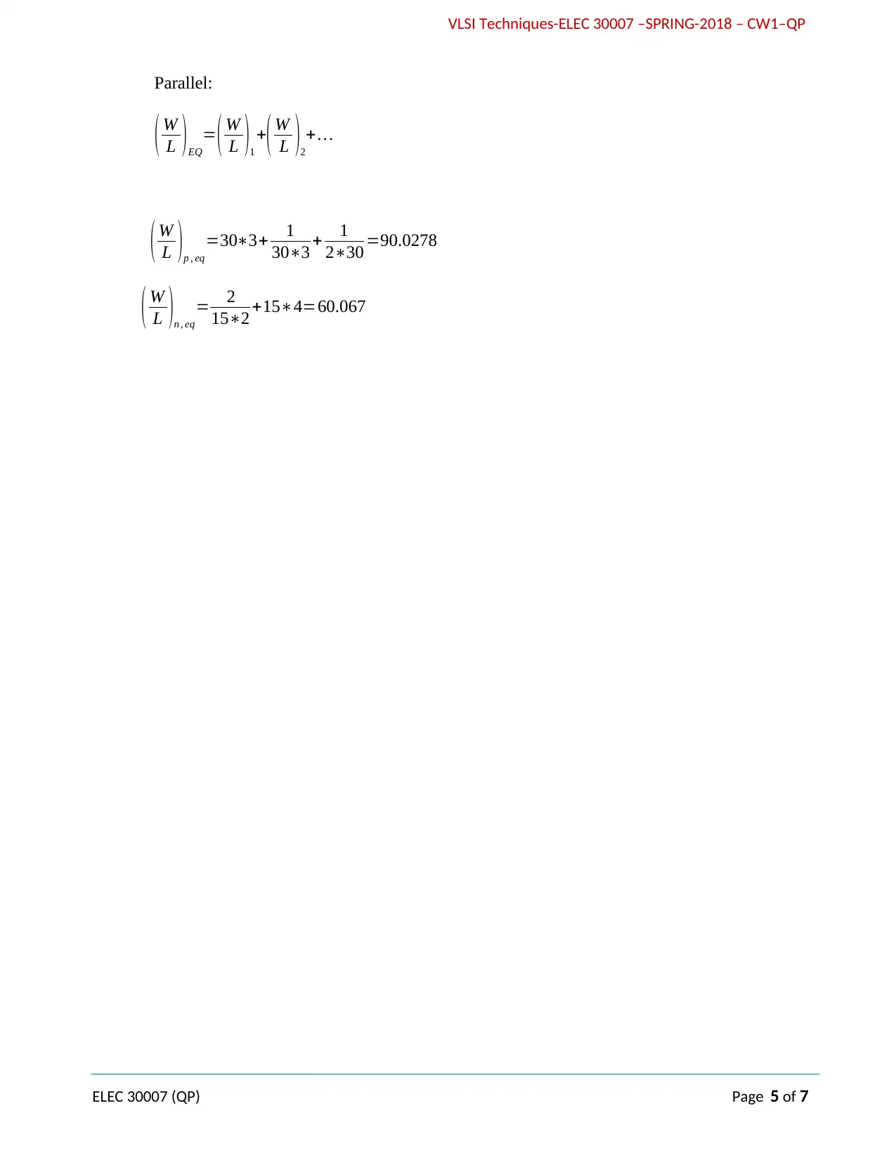
Parallel:
( W
L )EQ
= ( W
L )1
+( W
L )2
+…
( W
L )p , eq
=30∗3+ 1
30∗3 + 1
2∗30 =90.0278
( W
L )n , eq
= 2
15∗2 +15∗4=60.067
ELEC 30007 (QP) Page 5 of 7
Parallel:
( W
L )EQ
= ( W
L )1
+( W
L )2
+…
( W
L )p , eq
=30∗3+ 1
30∗3 + 1
2∗30 =90.0278
( W
L )n , eq
= 2
15∗2 +15∗4=60.067
ELEC 30007 (QP) Page 5 of 7
VLSI Techniques-ELEC 30007 –SPRING-2018 – CW1–QP
Reference
Chua, L. O., Gulak, G., Pierzchala, E., & Rodríguez-Vázquez, A. (1998). Cellular Neural Networks
and Analog VLSI. Boston, MA, Springer US. Available from:
http://public.eblib.com/choice/publicfullrecord.aspx?p=3087030. [Accessed 29th April 2018].
ICACCT. (2011) Comparative Analysis of Static and Dynamic CMOS Logic Design.
5th IEEE International Conference on Advanced Computing & Communication Technologies
ISBN 81-87885-03-3. [Accessed 29th April 2018].
IJISET. (2015) CMOS Half Adder Design & Simulation Using Different Foundry. International
Journal of Innovative Science, Engineering & Technology, Vol. 2. Available from:
www.ijiset.com [Accessed 29th April 2018].
Iniewski, K. (2013). CMOS nanoelectronics: analog and RF VLSI circuits. New York, McGraw-Hill.
http://accessengineeringlibrary.com/browse/cmos-nanoelectronics-analog-and-rf-vlsi-circuits.
[Accessed 29th April 2018].
IOSR-JVSP6. (2013) Analysis of CMOS Multiplexer Circuits of Different Area and Logic Style.
IOSR Journal of VLSI and Signal Processing () Volume 3, Issue, PP 17-27 e-ISSN: 2319 –
4200, p-ISSN No. : 2319 – 4197. Available from: www.iosrjournals.org [Accessed 29th April
2018].
Maloberti, F. (2001). Analog design for CMOS VLSI systems. Boston, Kluwer Academic.
VDAT (Symposium), Rahaman, H., Chattopadhyay, S., & Chattopadhyay, S. (2012). Progress in
VLSI design and test: 16th International Symposium, VDAT 2012, Shibpur, India, July 1-4,
2012. Proceedings. Berlin, Springer. Available from:
http://public.eblib.com/choice/publicfullrecord.aspx?p=3070263. [Accessed 29th April 2018].
ELEC 30007 (QP) Page 6 of 7
⊘ This is a preview!⊘
Do you want full access?
Subscribe today to unlock all pages.

Trusted by 1+ million students worldwide

VLSI Techniques-ELEC 30007 –SPRING-2018 – CW1–QP
Sachdev, M., Pineda De Gyvez, J., & Sachdev, M. (2007). Defect-oriented testing for nano-metric
CMOS VLSI circuits. Dordrecht, Springer. Available from:
http://public.eblib.com/choice/publicfullrecord.aspx?p=371648. [Accessed 29th April 2018].
ELEC 30007 (QP) Page 7 of 7
Sachdev, M., Pineda De Gyvez, J., & Sachdev, M. (2007). Defect-oriented testing for nano-metric
CMOS VLSI circuits. Dordrecht, Springer. Available from:
http://public.eblib.com/choice/publicfullrecord.aspx?p=371648. [Accessed 29th April 2018].
ELEC 30007 (QP) Page 7 of 7
1 out of 7
Your All-in-One AI-Powered Toolkit for Academic Success.
+13062052269
info@desklib.com
Available 24*7 on WhatsApp / Email
![[object Object]](/_next/static/media/star-bottom.7253800d.svg)
Unlock your academic potential
© 2024 | Zucol Services PVT LTD | All rights reserved.