ENG632d1 Electronics Assignment: FSM, Circuit Design & VHDL

Verified

Added on  2023/04/22

|22
|4497
|242
Homework Assignment
AI Summary
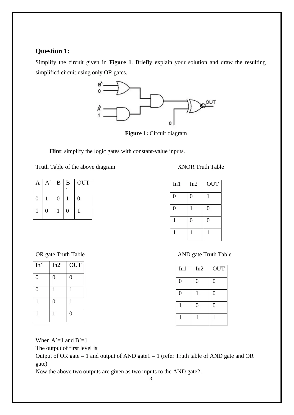
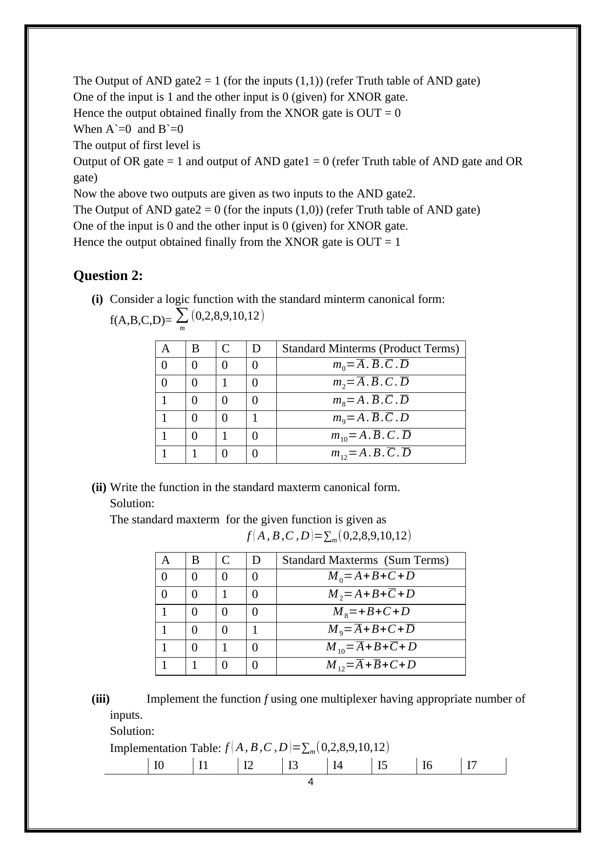
This assignment solution covers several key areas of electrical engineering, including circuit simplification using OR gates, logic function implementation using multiplexers and decoders, Boolean algebra simplification, Karnaugh map optimization, and VHDL modeling. It also includes the design of a Finite State Machine (FSM) for sequence detection and process control, utilizing D-type flip-flops and Logisim verification. Furthermore, the assignment delves into the analysis and VHDL implementation of an 8x32 register file. The document provides detailed explanations, truth tables, logic diagrams, VHDL code snippets, and state transition diagrams to illustrate the concepts and solutions. Desklib offers a wealth of similar resources to aid students in their studies.
Document Page
ELECTRICAL ENGINEERING
1
tabler-icon-diamond-filled.svg

Paraphrase This Document

Need a fresh take? Get an instant paraphrase of this document with our AI Paraphraser
Document Page
Table of Contents
Question 1:.................................................................................................................................................2
Question 2:.................................................................................................................................................3
Question 3:.................................................................................................................................................7
Question 4:.................................................................................................................................................8
Question 5:...............................................................................................................................................10
VHDL Code:........................................................................................................................................11
Block Diagram of Shift Register:.......................................................................................................12
Test Bench Program:..........................................................................................................................14
Question 6:...............................................................................................................................................14
VHDL code:.........................................................................................................................................16
References................................................................................................................................................18
2
Document Page
Question 1:
Simplify the circuit given in Figure 1. Briefly explain your solution and draw the resulting
simplified circuit using only OR gates.
Figure 1: Circuit diagram
Hint: simplify the logic gates with constant-value inputs.
Truth Table of the above diagram XNOR Truth Table
A A` B B
`
OUT
0 1 0 1 0
1 0 1 0 1
OR gate Truth Table AND gate Truth Table
When A`=1 and B`=1
The output of first level is
Output of OR gate = 1 and output of AND gate1 = 1 (refer Truth table of AND gate and OR
gate)
Now the above two outputs are given as two inputs to the AND gate2.
3
In1 In2 OUT
0 0 1
0 1 0
1 0 0
1 1 1
In1 In2 OUT
0 0 0
0 1 1
1 0 1
1 1 0
In1 In2 OUT
0 0 0
0 1 0
1 0 0
1 1 1
Document Page
The Output of AND gate2 = 1 (for the inputs (1,1)) (refer Truth table of AND gate)
One of the input is 1 and the other input is 0 (given) for XNOR gate.
Hence the output obtained finally from the XNOR gate is OUT = 0
When A`=0 and B`=0
The output of first level is
Output of OR gate = 1 and output of AND gate1 = 0 (refer Truth table of AND gate and OR
gate)
Now the above two outputs are given as two inputs to the AND gate2.
The Output of AND gate2 = 0 (for the inputs (1,0)) (refer Truth table of AND gate)
One of the input is 0 and the other input is 0 (given) for XNOR gate.
Hence the output obtained finally from the XNOR gate is OUT = 1
Question 2:
(i) Consider a logic function with the standard minterm canonical form:
f(A,B,C,D)=
m
(0,2,8,9,10,12)
(ii) Write the function in the standard maxterm canonical form.
Solution:
The standard maxterm for the given function is given as
f ( A , B ,C , D ) =m (0,2,8,9,10,12)
(iii) Implement the function f using one multiplexer having appropriate number of
inputs.
Solution:
Implementation Table: f ( A , B ,C , D )=m (0,2,8,9,10,12)
I0 I1 I2 I3 I4 I5 I6 I7
4
A B C D Standard Minterms (Product Terms)
0 0 0 0 m0= A . B .C . D
0 0 1 0 m2= A . B . C . D
1 0 0 0 m8= A . B .C . D
1 0 0 1 m9= A . B .C . D
1 0 1 0 m10= A . B . C . D
1 1 0 0 m12= A . B . C . D
A B C D Standard Maxterms (Sum Terms)
0 0 0 0 M 0= A+B+C +D
0 0 1 0 M 2= A+B+C +D
1 0 0 0 M 8=+B+C + D
1 0 0 1 M 9= A+ B+C + D
1 0 1 0 M 10= A+B+C+ D
1 1 0 0 M 12=A + B+C+D
tabler-icon-diamond-filled.svg

Paraphrase This Document

Need a fresh take? Get an instant paraphrase of this document with our AI Paraphraser
Document Page
A’
1 3 4 5 6 7
A
11 13 14 15
1 A 1 0 A 0 0 0
The output of 8:1 Mux are given as,
I0 = I2 = 1 (logic 1)
I1 = I4 = A
I3 = I5 = I6 = I7 = 0 (logic 0)
8:1 MUX :
(iv)Implement the function f using one decoder having appropriate number of inputs, and a
logic gate.
Solution: f ( A , B ,C , D ) =m (0,2,8,9,10,12)
5
0
8 9 10
2
12
I0
I1
I2
I3
8:1 MUX Y
I4
I5
I6
I7
S2 S1 S0
Logic 1
A
Logic 0
F
B
C
D
I0
I1
I2
I3
A 4 – to – 16 I4
B Decoder I5
CI6
DI7
I8
I9
I10
I11
I12
I13
I14I15
Document Page
(v) Write the logical expression of the function f.
The logical expression of the function f ( A , B ,C , D ) =m (0,2,8,9,10,12) is given as
f = A . B . C . D+ A . B . C . D+ A . B . C . D+A . B . C . D+ A . B .C . D+ A . B .C . D
(vi)Using Boolean algebra rules, give the most simplified logical expression of the function
f. Show the details of your work.
Solution:
Simplified logical expression of the function f ( A , B ,C , D ) =m (0,2,8,9,10,12) is
given as
f = A . B . C . D+ A . B . C . D+ A . B . C . D+A . B . C . D+ A . B .C . D+ A . B .C . D
f = ( A . B . C . D+ A . B . C . D ) + ( A . B . C . D+ A . B . C . D ) + A . B .C . D+ A . B .C . D
f = A . B . D ( C .+C . ) + A . B .C ( D+D )+ A . B .C . D+ A . B .C . D [ Boolean rule: C .+C=1]
f = A . B . D+ A . B . C+ A . B .C . D+ A . B .C . D
(vii) Using Karnaugh map, give the most simplified logical expression of the function
f. Show the details of your work.
00 01 11 10
00 1 1
01
11 1
10 1 1 1
Grouping 1
¿ A . B . C . D+ A . B . C . D+ A . B . C . D+ A . B .C . D= A . B . D ( C +C ) + A . B . D ( C +C ) =A . B . D+ A . B . D=B . D
Grouping 2¿ A . B . C . D+ A . B . C . D= A . C . D ( B+B ) = A .C . D
Grouping 3¿ A . B . C . D+ A . B . C . D= A . B . C ( D+D ) =A . B . C
f =B . D+ A . C . D+ A . B . C
6
AB
CD
Gropuping1
Gropuping2 Gropuping3
Document Page
(viii)Using the most simplified logical expression of the function f, draw the resulting circuit
of the function using only NAND gates (even to generate the inverse of an input).
f =B . D+ A . C . D+ A . B . C
Logic Diagram:
(ix)Write a VHDL entity to model the function f.
library ieee;
use ieee.std_logic_1164.all;
entity digm is
port (A,B,C,D: in std_logic;
f:out std_logic);
end digm;
architecture digmarch of digm is
component not1
port(B:in std_logic; Bbar: out std_logic);
end component;
component not2
port(C:in std_logic; Cbar: out std_logic);
end component;
7
B’
D’
C’
D’
A
C’
B’
A
tabler-icon-diamond-filled.svg

Paraphrase This Document

Need a fresh take? Get an instant paraphrase of this document with our AI Paraphraser
Document Page
component not3
port(D:in std_logic; Dbar: out std_logic);
end component;
component and1
port(Bbar,Dbar:in std_logic; x1: out std_logic);
end component;
component and2
port(A,Cbar,Dbar:in std_logic; x2: out std_logic);
end component;
component and3
port(A,Cbar,Dbar:in std_logic; x3: out std_logic);
end component;
component or1
port(x1,x2,x3:in std_logic; y: out std_logic);
end component;
begin
F1:or1 port map(x1,x2,x3,y);
end digmarch;
Question 3:
A sequence detector has a single binary input and a single binary output. The output of the
detector should turn immediately to logic 1 when the pattern 0110 is received in the input stream
with overlap patterns. Here is an example of input-output sequence:
Input : 111011011011
Output : 000000100100
8
a/1
b/0
d/0
c/0
1
0
00
11
0
Document Page
Give a Finite State Machine (FSM) transition diagram of the above system.
Solution:
The above diagram gives the transition diagram of the system.
In order to obtain the repeated sequence ‘0110’, the system is designed with states.
Consider there are 4 states in the system. a,b,c and d with two inputs 0 and 1.
The system starts with the initial state ‘a’.
When the input is 0, the system enters into the next state ‘b’ with output 0. And when
the input is 1, the system remains in the same state with output 0.
Now the next state ‘b’ is considered.
When the input of state ‘b’ is 0, the system remains in the same state. And when the input
is 1, the system enters into the next state.
Next the system enters the state ‘c’.
When the input to the system is 1, the system enters the next state’s’. And when the input
is 0, the sequence is not in order. Therefore, again the system enters into the state ‘a’.
Finally the system enters into the state ‘d’.
When the input is 0, the sequence gets completed as ‘0110’. Therefore, the system
produces the output 1 and again it resets to repeat the sequence.
Question 4:
Figure 4 gives the diagram of a Finite State Machine (FSM) used in a process control system.
The FSM has one input, one output and three states.
9
Document Page
Figure 4: FSM diagram
(i) Name the model of the above FSM. Explain your answer.
The model describes the state machine in the automation process (Rani, Fatima, Kalra &
Sinha, 2017).
The system works in a sequence. There are three states in the FSM. Each state has its
own criteria. If it is satisfied, the state proceeds with the next state. Else it maintain in the
same state, till it reaches the condition.
(ii) Design an efficient digital circuit of this FSM using D-type flip-flops. In your answer,
you should include the following:
Input Present state Next State Flip – Flop Input
X A B A+1 B+1 DA DB
0 0 0 0 0 0 0
0 0 1 1 0 1 0
0 1 0 0 0 0 0
0 1 1 1 0 1 0
1 0 0 0 1 0 1
1 0 1 0 1 0 1
1 1 0 1 1 1 1
1 1 1 0 1 0 1
10
tabler-icon-diamond-filled.svg

Paraphrase This Document

Need a fresh take? Get an instant paraphrase of this document with our AI Paraphraser
Document Page
(a) State transition table
Present state
Next state
x=0 x=1
S0 S0 S2
S1 S1 S2
S2 S1 S2
(b) Karnaugh maps to get simplified logical expressions of the D flip-flops inputs and the
FSM output.
Let us consider the present states as : A and B and the next state as A+1 and B+1 with
input x.
DA DB
00 01 11 10
0 0 1 1 0
1 0 0 0 1
DB=x A + xBA
DA=x
(iii) Verify in Logisim software the correctness of your designed digital circuit.
Discuss the results of your simulation. (The Logisim design circuit and simulation log
file should be both submitted.)
11
AB
x
AB
00 01 11 10
0 0 0 0 0
1 1 1 1 1
x
Document Page
Question 5:
Figure 5.2 gives the internal structure of the 8x32 Register file shown in Figure 5.1.
The structure has an internal array of eight 32-bit registers where data is stored. It allows two
simultaneous combinational reads from the array of registers. The inputs “Rs” and “Rt” select
the two array registers whose values are set on “Rs_output” and “Rt_output”, respectively. The
structure allows one synchronous write operation on the registers array when the enable signal
“Regwrite” is set to one; the value of “Rd” selects the element of the registers array to update
with the value of “Rd_Data”.
Figure 5.1: Register file interface
12
chevron_up_icon
1 out of 22
circle_padding
hide_on_mobile
zoom_out_icon
[object Object]