Analysis of Zener Diode and Switching Power Conversion in Electronics
VerifiedAdded on 2023/05/29
|34
|5259
|413
Report
AI Summary
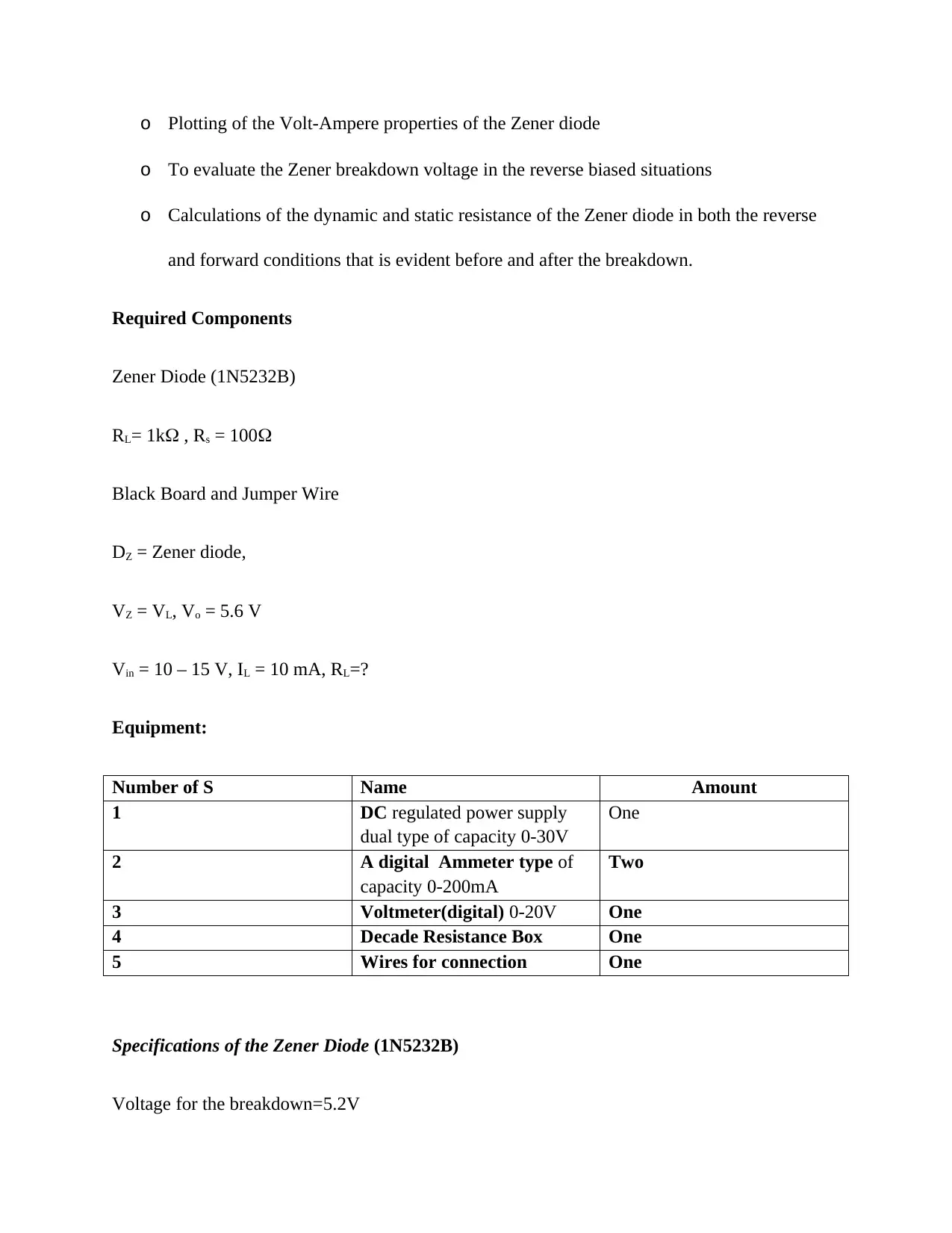
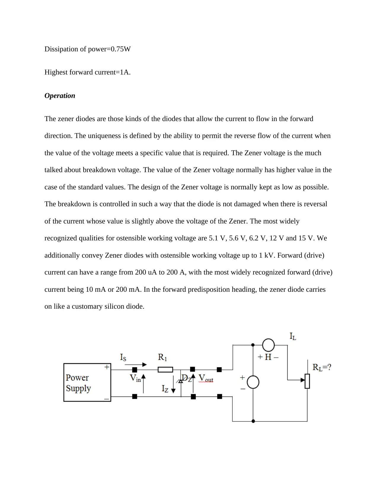
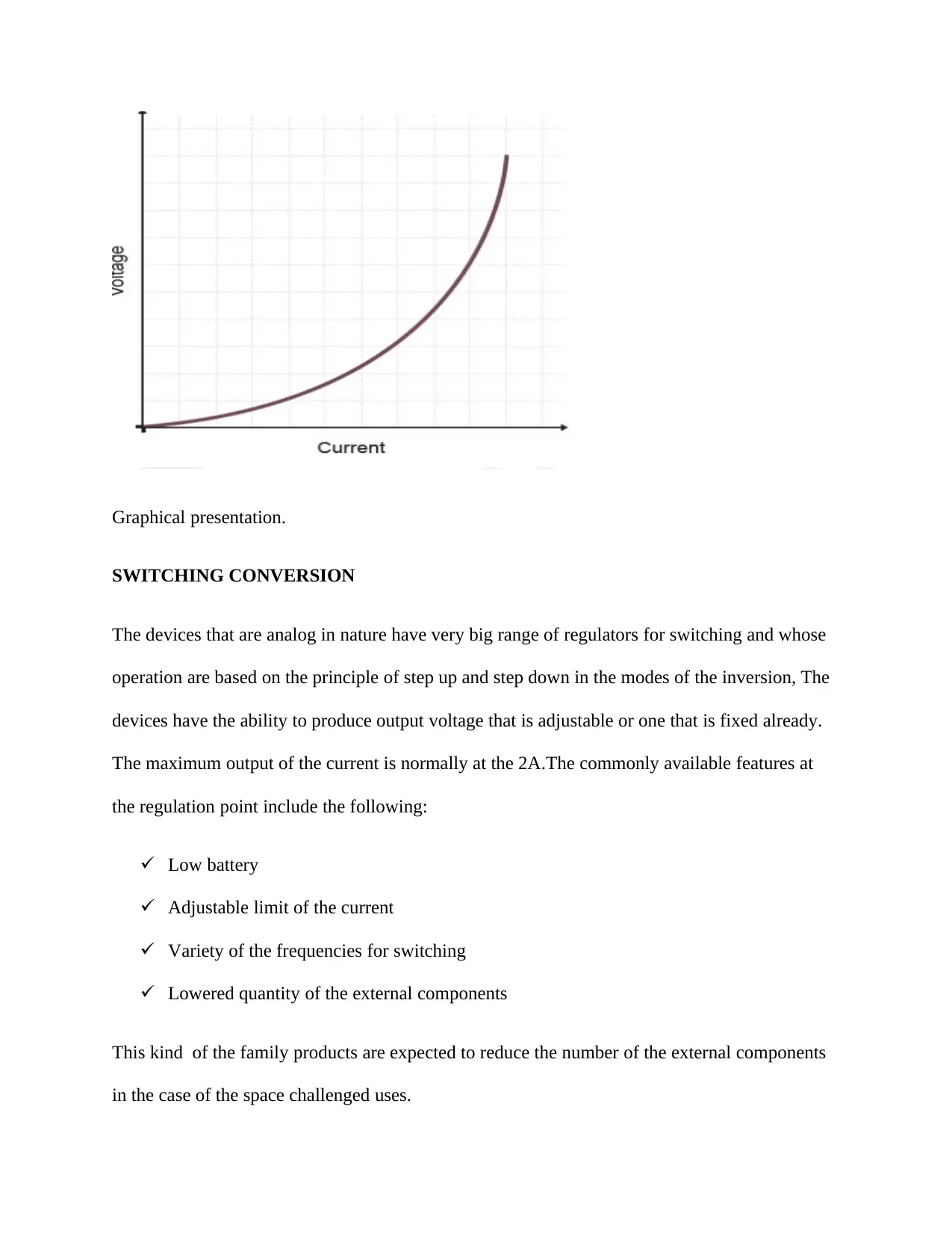
This report delves into the characteristics and applications of Zener diodes and switching power conversion techniques. It begins with an introduction to Zener diodes, explaining their behavior in both forward and reverse bias conditions, including the Zener breakdown voltage and its significance in voltage regulation. The report outlines an experiment designed to analyze the Volt-Ampere properties of a Zener diode, determine its breakdown voltage, and calculate its dynamic and static resistance. It then transitions to switching power conversion, discussing the operation of buck, boost, and buck-boost converters, highlighting their advantages in terms of efficiency and space utilization. The report details the components of switching circuits and explores the use of these converters in various applications, including the generation of fixed or adjustable output voltages. The document also includes circuit diagrams, experimental procedures, and results, along with a graphical representation of the findings, providing a comprehensive overview of both Zener diodes and switching power conversion principles. The report concludes by emphasizing the importance of these technologies in modern power electronics.
1 out of 34
Related Documents


Your All-in-One AI-Powered Toolkit for Academic Success.
+13062052269
info@desklib.com
Available 24*7 on WhatsApp / Email
![[object Object]](/_next/static/media/star-bottom.7253800d.svg)
Copyright © 2020–2026 A2Z Services. All Rights Reserved. Developed and managed by ZUCOL.