Analysis of 555 Timer Circuits: PWM, Analog Circuits and Filter Design
VerifiedAdded on 2019/12/04
|17
|3580
|857
Report
AI Summary
This report provides a comprehensive analysis of the 555 timer integrated circuit (IC), a fundamental component in electronics design. It explores the 555 timer's functionality in various modes, including monostable, astable, and bistable. The report delves into a specific oscillator circuit design that allows for wide duty cycle control without affecting the frequency, along with the mathematical proof behind its operation. It also discusses the use of an air-variable capacitor for frequency control. Furthermore, the report examines the application of PWM (Pulse Width Modulation) techniques, including its use in driving inertial loads, communication, and lighting systems, and the techniques for improving PWM resolution. It contrasts analog and digital control methods, highlighting the advantages of PWM in terms of cost, power consumption, and noise immunity. The report also touches upon filter design, emphasizing their importance in signal processing systems, and the trade-offs involved in designing PWM carrier frequencies to minimize harmonic ripple. The content underscores the 555 timer's versatility and its significance in various electronic applications, providing valuable insights into its design and implementation.
Introduction
The 555 timer integrated circuit (IC) has become a mainstay in electronics design.
A 555 timer will produce a pulse when a trigger signal is applied to it. The pulse
length is determined by the amount of time it takes to charge and discharge a
capacitor connected to a 555 timer. A 555 timer can be used to denounce switches,
Modulate signals, create accurate clock signals, create pulse width modulated
(PWM) signals, etc. A 555 timer can be obtained from various manufacturers
including Fairchild Semiconductor and National Semiconductor.
The 555 timer can operate in 3 different modes:
i. Monostable Mode
ii. Astable Mode or free running
iii. Bistable Mode or Schmitt Trigger
Designs
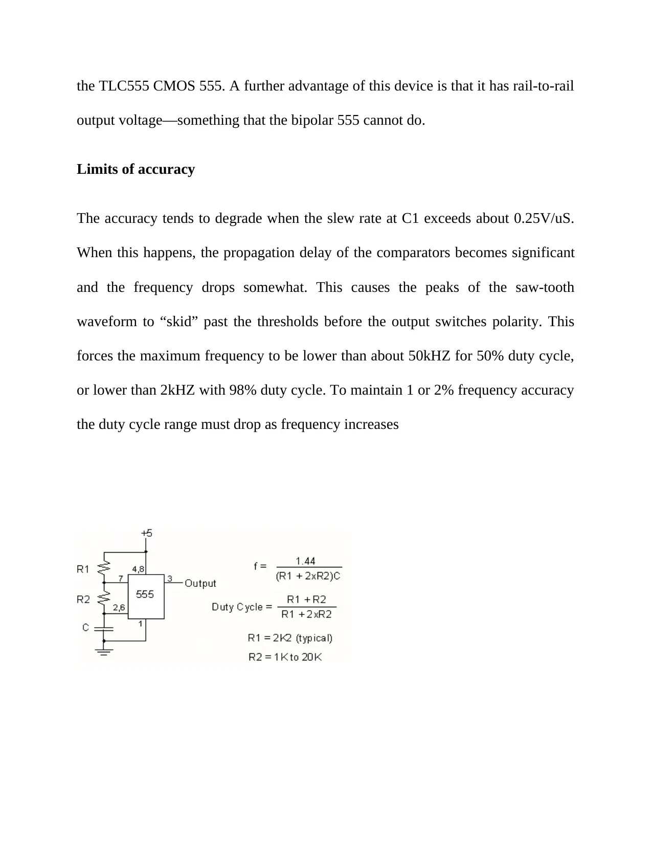
Here is a simple oscillator circuit that varies the duty cycle over a wide range
without affecting the frequency. It is a variation of the simple 555 astable
oscillator. Initially, I told a reader that there was no standard 555 circuit that could
do this, but then the grey matter started working. The use of an air-variable
Paraphrase This Document
Need a fresh take? Get an instant paraphrase of this document with our AI Paraphraser
capacitor for frequency control is a mind-blower—nothing short of a time warp!
555 Duty Cycle Control Schematic
Overview
When potentiometer R1 is centered, operation is obvious and the duty cycle is
50%. However, as R1 is rotated in either direction the charge time and discharge
times vary accordingly. The two sides of R1 have independent steering diodes (D1
& D2). C1 & C2 make up the timing capacitor. Pins 2 & 6 of the 555 are the upper
and lower thresholds of the input comparators. The charge /discharge voltage is
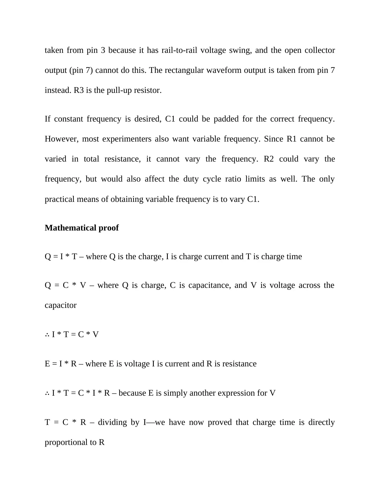
taken from pin 3 because it has rail-to-rail voltage swing, and the open collector
output (pin 7) cannot do this. The rectangular waveform output is taken from pin 7
instead. R3 is the pull-up resistor.
If constant frequency is desired, C1 could be padded for the correct frequency.
However, most experimenters also want variable frequency. Since R1 cannot be
varied in total resistance, it cannot vary the frequency. R2 could vary the
frequency, but would also affect the duty cycle ratio limits as well. The only
practical means of obtaining variable frequency is to vary C1.
Mathematical proof
Q = I * T – where Q is the charge, I is charge current and T is charge time
Q = C * V – where Q is charge, C is capacitance, and V is voltage across the
capacitor
∴ I * T = C * V
E = I * R – where E is voltage I is current and R is resistance
∴ I * T = C * I * R – because E is simply another expression for V
T = C * R – dividing by I—we have now proved that charge time is directly
proportional to R
⊘ This is a preview!⊘
Do you want full access?
Subscribe today to unlock all pages.

Trusted by 1+ million students worldwide
So we have a charge resistance and a discharge resistance, the sum of which is
constant and equal to the R1 potentiometer total resistance (1 to 3). Therefore, the
sum of the charge and discharge times is also constant. Since F = 1/T, the
frequency is also be constant.
In other words, the two resistances are complementary and the two time periods
are likewise complementary.
The Air Variable Capacitor
The old-fashioned air variable capacitor is old and klunky. While DigiKey offers
no such product, these devices remain available on eBay as used or old stock.
Every serious experimenter should have one of these. The one I would buy is a 3-
gang 440pf. Wired in parallel the total capacitance is 1320pf. Physical size
limitations prevent higher capacitances.
Actually, it is fun to play with air variable capacitors.
High impedances
To obtain a reasonably low frequency, R1 had to be selected to have as high a
resistance as possible. 2M is the highest value pot I had on hand. A 5M would also
be a good selection. To function under such high impedance conditions, I selected
Paraphrase This Document
Need a fresh take? Get an instant paraphrase of this document with our AI Paraphraser
the TLC555 CMOS 555. A further advantage of this device is that it has rail-to-rail
output voltage—something that the bipolar 555 cannot do.
Limits of accuracy
The accuracy tends to degrade when the slew rate at C1 exceeds about 0.25V/uS.
When this happens, the propagation delay of the comparators becomes significant
and the frequency drops somewhat. This causes the peaks of the saw-tooth
waveform to “skid” past the thresholds before the output switches polarity. This
forces the maximum frequency to be lower than about 50kHZ for 50% duty cycle,
or lower than 2kHZ with 98% duty cycle. To maintain 1 or 2% frequency accuracy
the duty cycle range must drop as frequency increases
PWM designs
The PWM is a technique which is used to drive the inertial loads since a very long
time. The simple example of an inertial load is a motor. Apply the power to a
motor for a very short period of time and then turn off the power: it can be
observed that the motor is still running even after the power has been cut off from
it. This is due to the inertia of the motor and the significance of this factor is that
the continuous power is not required for that kind of devices to operate. A burst
power can save the total power supplied to the load while achieving the same
performance from the device as it runs on continuous power. The PWM technique
is use in devices like DC motors, Loudspeakers, Class -D Amplifiers etc. They are
also used in communication field as-well. The modulation techniques like AM, FM
are widely used RF communication whereas the PWM is modulation technique is
mostly used in Optical Fiber Communication (OFC). As in the case of the inertial
loads mentioned previously, the PWM in a communication link greatly saves the
transmitter power. The immunity of the PWM transmission against the inter-
symbol interference is another advantage. This article discusses the technique of
generating a PWM wave corresponding to a modulating sine wave. PWM can be
used in the lighting system to reduce the need for DC/DC voltage conversions.
PWM can also be employed to reduce the destructive effect of arcing. In motor
systems, PWM can be used to perform both voltage conversion and speed control.
⊘ This is a preview!⊘
Do you want full access?
Subscribe today to unlock all pages.

Trusted by 1+ million students worldwide
This paper will show the results of testing of PWM in these applications. One
approach for improving the duty cycle resolution is to decrease the carrier
frequency of the PWM. In the previous example, reducing the carrier frequency to
50 kHz from 100 kHz cuts the step size in half to 1.65 mV (i.e. ~11 bits resolution
in standard resolution PWM mode, ~17 bits resolution in high resolution PWM
mode). However, the lower carrier frequency also decreases the base frequency of
the unwanted harmonics in equation (1). In particular, the first harmonic will now
appear at 50 kHz rather than 100 kHz, and more of it will pass through the analog
low-pass filter, thereby increasing the harmonic ripple. Methods for reducing the
harmonic ripple involve modifying the analog low-pass filter to increase the stop-
band roll-off (i.e., a higher order filter) or to decrease the pass-band cut-off
frequency. Both of these methods have drawbacks however. Increasing the stop-
band roll-off generally means a more complex analog filter circuit, and
correspondingly a higher cost. Alternately, decreasing the pass-band cut-off
frequency also decreases the bandwidth of the DAC. In other words, the DAC is
limited in bandwidth by the bandwidth of the analog low-pass filter. For a given
analog low-pass filter, it is clear that a trade-off exists between harmonic ripple
and PWM duty cycle resolution when selecting the PWM carrier frequency. The
optimal carrier frequency is the one where the total uncertainty is smallest
Paraphrase This Document
Need a fresh take? Get an instant paraphrase of this document with our AI Paraphraser
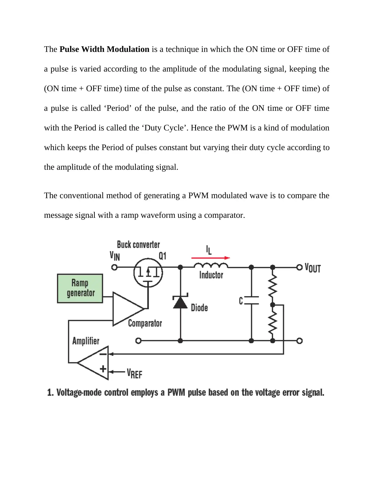
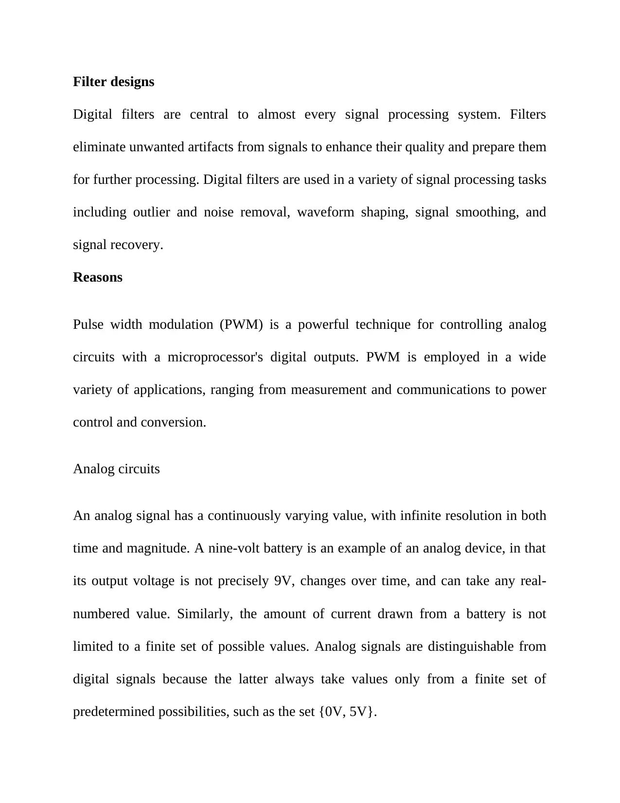
The Pulse Width Modulation is a technique in which the ON time or OFF time of
a pulse is varied according to the amplitude of the modulating signal, keeping the
(ON time + OFF time) time of the pulse as constant. The (ON time + OFF time) of
a pulse is called ‘Period’ of the pulse, and the ratio of the ON time or OFF time
with the Period is called the ‘Duty Cycle’. Hence the PWM is a kind of modulation
which keeps the Period of pulses constant but varying their duty cycle according to
the amplitude of the modulating signal.
The conventional method of generating a PWM modulated wave is to compare the
message signal with a ramp waveform using a comparator.
Filter designs
Digital filters are central to almost every signal processing system. Filters
eliminate unwanted artifacts from signals to enhance their quality and prepare them
for further processing. Digital filters are used in a variety of signal processing tasks
including outlier and noise removal, waveform shaping, signal smoothing, and
signal recovery.
Reasons
Pulse width modulation (PWM) is a powerful technique for controlling analog
circuits with a microprocessor's digital outputs. PWM is employed in a wide
variety of applications, ranging from measurement and communications to power
control and conversion.
Analog circuits
An analog signal has a continuously varying value, with infinite resolution in both
time and magnitude. A nine-volt battery is an example of an analog device, in that
its output voltage is not precisely 9V, changes over time, and can take any real-
numbered value. Similarly, the amount of current drawn from a battery is not
limited to a finite set of possible values. Analog signals are distinguishable from
digital signals because the latter always take values only from a finite set of
predetermined possibilities, such as the set {0V, 5V}.
⊘ This is a preview!⊘
Do you want full access?
Subscribe today to unlock all pages.

Trusted by 1+ million students worldwide
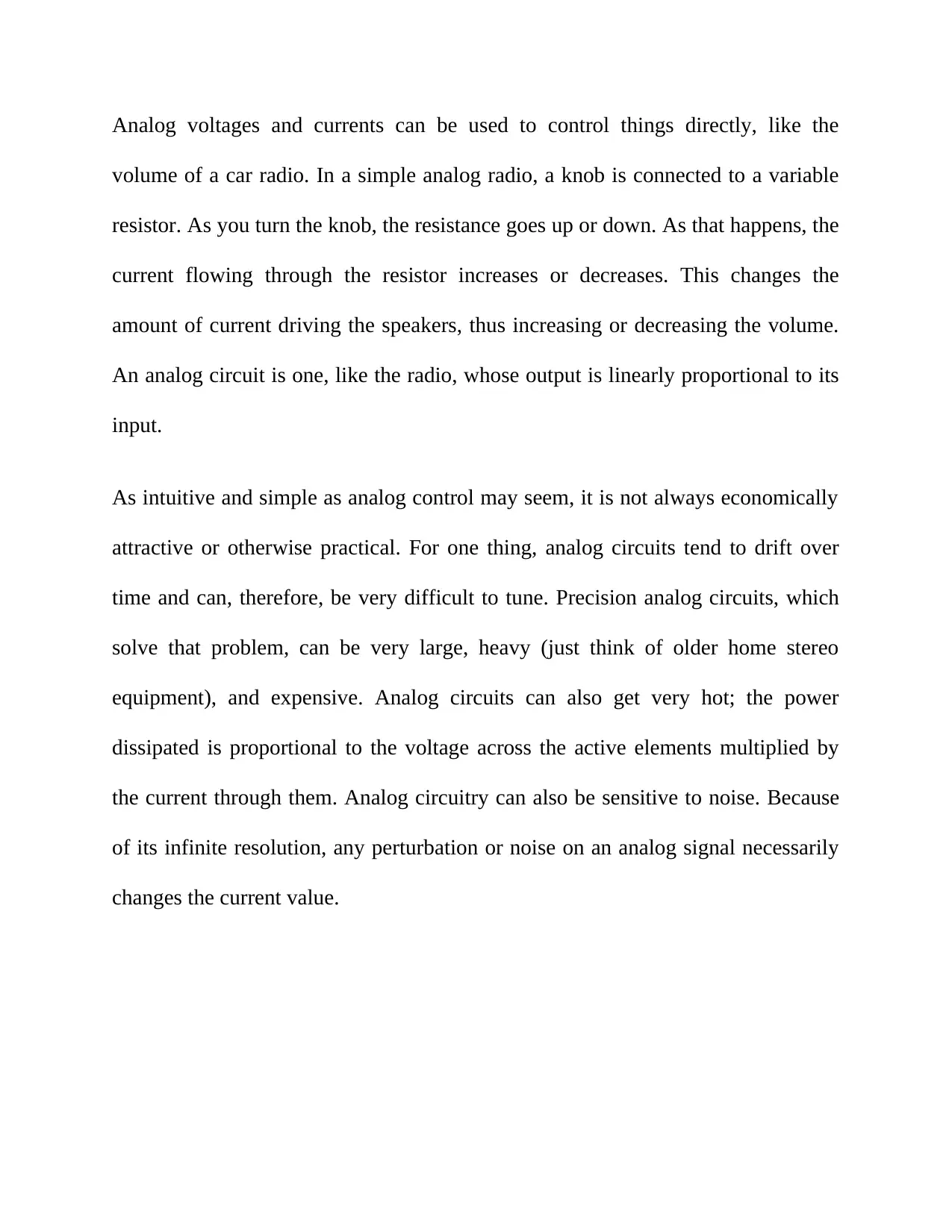
Analog voltages and currents can be used to control things directly, like the
volume of a car radio. In a simple analog radio, a knob is connected to a variable
resistor. As you turn the knob, the resistance goes up or down. As that happens, the
current flowing through the resistor increases or decreases. This changes the
amount of current driving the speakers, thus increasing or decreasing the volume.
An analog circuit is one, like the radio, whose output is linearly proportional to its
input.
As intuitive and simple as analog control may seem, it is not always economically
attractive or otherwise practical. For one thing, analog circuits tend to drift over
time and can, therefore, be very difficult to tune. Precision analog circuits, which
solve that problem, can be very large, heavy (just think of older home stereo
equipment), and expensive. Analog circuits can also get very hot; the power
dissipated is proportional to the voltage across the active elements multiplied by
the current through them. Analog circuitry can also be sensitive to noise. Because
of its infinite resolution, any perturbation or noise on an analog signal necessarily
changes the current value.
Paraphrase This Document
Need a fresh take? Get an instant paraphrase of this document with our AI Paraphraser
Digital control
By controlling analog circuits digitally, system costs and power consumption can
be drastically reduced. What's more, many microcontrollers and DSPs already
include on-chip PWM controllers, making implementation easy.
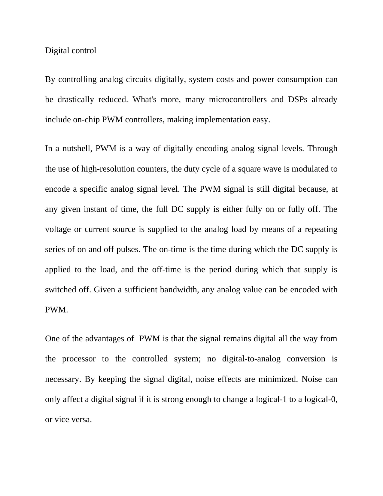
In a nutshell, PWM is a way of digitally encoding analog signal levels. Through
the use of high-resolution counters, the duty cycle of a square wave is modulated to
encode a specific analog signal level. The PWM signal is still digital because, at
any given instant of time, the full DC supply is either fully on or fully off. The
voltage or current source is supplied to the analog load by means of a repeating
series of on and off pulses. The on-time is the time during which the DC supply is
applied to the load, and the off-time is the period during which that supply is
switched off. Given a sufficient bandwidth, any analog value can be encoded with
PWM.
One of the advantages of PWM is that the signal remains digital all the way from
the processor to the controlled system; no digital-to-analog conversion is
necessary. By keeping the signal digital, noise effects are minimized. Noise can
only affect a digital signal if it is strong enough to change a logical-1 to a logical-0,
or vice versa.
Increased noise immunity is yet another benefit of choosing PWM over analog
control, and is the principal reason PWM is sometimes used for communication.
Switching from an analog signal to PWM can increase the length of a
communications channel dramatically. At the receiving end, a suitable RC
(resistor-capacitor) or LC (inductor-capacitor) network can remove the modulating
high frequency square wave and return the signal to analog form.
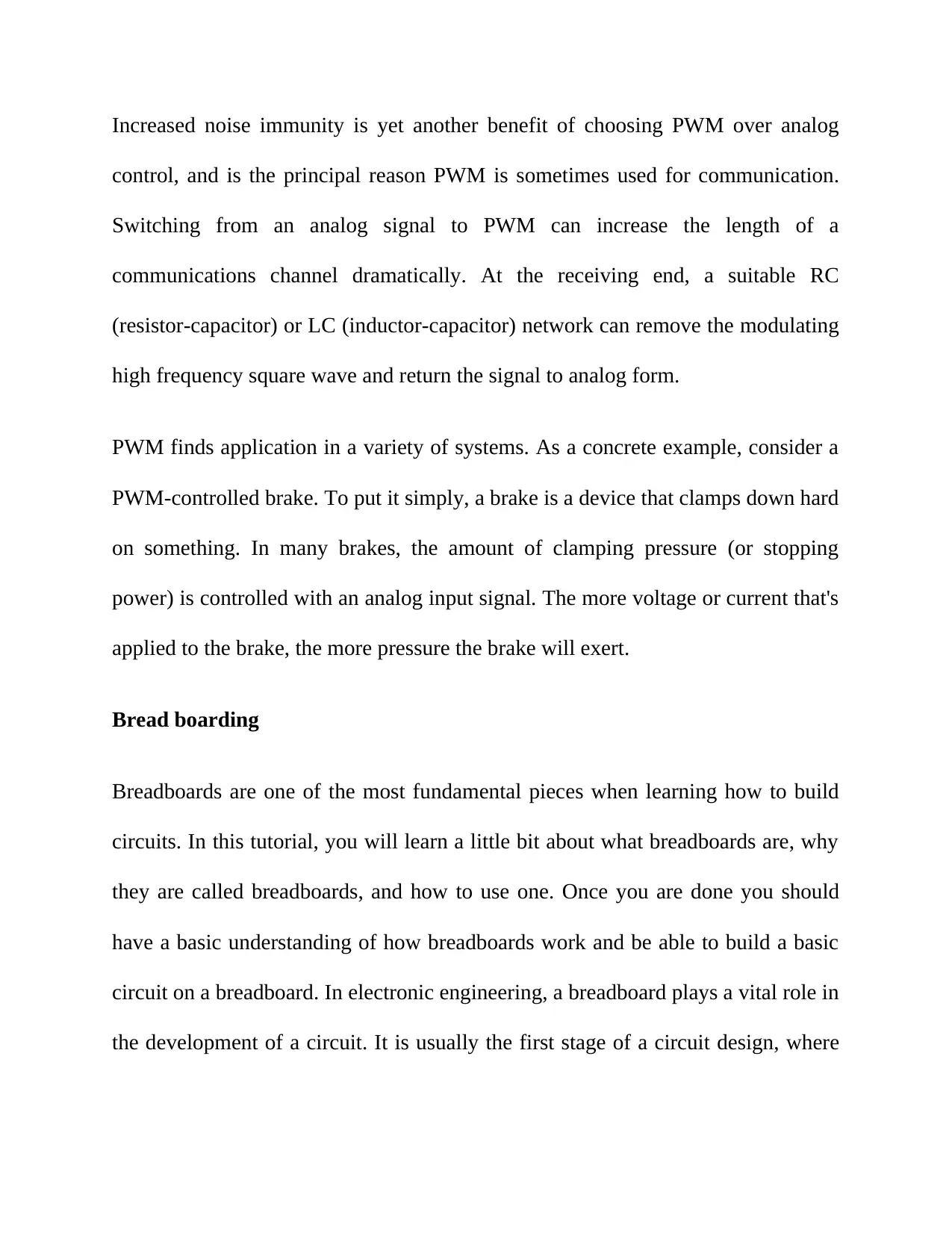
PWM finds application in a variety of systems. As a concrete example, consider a
PWM-controlled brake. To put it simply, a brake is a device that clamps down hard
on something. In many brakes, the amount of clamping pressure (or stopping
power) is controlled with an analog input signal. The more voltage or current that's
applied to the brake, the more pressure the brake will exert.
Bread boarding
Breadboards are one of the most fundamental pieces when learning how to build
circuits. In this tutorial, you will learn a little bit about what breadboards are, why
they are called breadboards, and how to use one. Once you are done you should
have a basic understanding of how breadboards work and be able to build a basic
circuit on a breadboard. In electronic engineering, a breadboard plays a vital role in
the development of a circuit. It is usually the first stage of a circuit design, where
⊘ This is a preview!⊘
Do you want full access?
Subscribe today to unlock all pages.

Trusted by 1+ million students worldwide
1 out of 17
Related Documents
Your All-in-One AI-Powered Toolkit for Academic Success.
+13062052269
info@desklib.com
Available 24*7 on WhatsApp / Email
![[object Object]](/_next/static/media/star-bottom.7253800d.svg)
Unlock your academic potential
Copyright © 2020–2026 A2Z Services. All Rights Reserved. Developed and managed by ZUCOL.


