Analogue Electronic Circuits: Diode and BJT Analysis Report
VerifiedAdded on 2023/01/23
|20
|3810
|98
Report
AI Summary
This report provides a comprehensive analysis of analogue electronic circuits, focusing on the characteristics and applications of diodes and bipolar junction transistors (BJTs). The study begins with an introduction to electronic devices and their significance in signal amplification and rectification. It then delves into the theoretical explanations of NPN bipolar transistors and diodes, emphasizing their key properties. The report utilizes Multisim software for simulation and analysis, enhancing the understanding of theoretical concepts through practical experimentation. The diode section covers forward and reverse bias operations, including the effects of voltage on current flow. It also explores diode rectification, including half-wave and full-wave rectification circuits, and discusses output smoothing techniques. The BJT section examines input and output characteristics, along with the different operating regions. The results and analysis section presents experimental data obtained from Multisim simulations, showcasing the voltage-current characteristics of diodes under forward and reverse bias conditions. Graphical representations of the data are provided to illustrate the behavior of diodes and the impact of biasing voltage. The report also details the construction and analysis of diode rectifier circuits, including half-wave rectifiers, and their input/output waveforms. This assignment demonstrates a strong understanding of fundamental electronic components and their applications in circuit design.

Analogue Electronic Circuits 1
Student
Instructor
Analogue and digital electronics
Date
Student
Instructor
Analogue and digital electronics
Date
Paraphrase This Document
Need a fresh take? Get an instant paraphrase of this document with our AI Paraphraser
Analogue Electronic Circuits 2
Introduction
Electronic devices over the recent past have been extensively applied in signal amplification as well
as signal rectification applications. It is very fundamental for one to understand in-depth
characteristics of commonly used electronic semiconductor devices like transistors and diodes for
appropriate applications for the same. This report dealt with theoretical explanation of common
characteristics of NPN bipolar transistor (BJT) and a diode and their applications. Using Multisim
software, theoretical knowledge have been enhanced by simulation and analysis. Experimental data
were recorded and represented in graphical means.
Diodes
A diode is a solid state electrical device structurally made of a P-N junction that permits
unidirectional flow of current. The P-N type diode is made of two materials such that in the N-region,
electrons are the majority charge carriers while in the P-region, the majority charge carriers are holes.
Holes are regions are positively charged segments whose electrons were depleted (Eric Gregersen
2019). The two regions are separated by an interface commonly known as depletion region. The
depletion region is formed when intermediate electrons at the junction diffuse from N-region into a
portion of P-region to fill holes which thereafter stops further electrons from entering P-region. This
process occurs during doping. In doping process, the negative side of the diode also known as cathode
is made of the materials that easily displaces excess electrons while the positive side, referred to as
anode, is made of the materials that easily accepts electrons due to holes (J.M.K.C. Donev et al.
2018).
There are two modes of diode operations namely; forward and reverse bias. In forward bias, a diode
will let current flow through it. On the contrary, the current will not flow in reverse bias within
diode’s capability. An ideal diode should allow current to flow through it freely without offering any
resistance. Under an ideal condition therefore, there should be no voltage drop across the diode when
operating in forward bias mode. In the same light, an ideal diode should offer infinite resistance to
flow of current when operated in reverse bias mode. This is not the case with the practical diode
because it possess a small resistive characteristics when operated in forward bias mode, thereby
leading to a fractional voltage drop across it (All About Circuits 2018). Theoretically, voltage drop
across the diode is about 0.7V for silicon diode.
Forward biasing of diodes
Operation of the diode in forward biasing mode is effected when the anode of the battery is connected
to the anode (P-region terminal) of the diode and cathode of the battery is connected with the N-
region (cathode). For the practical case, the diode will only conduct if the biasing voltage supersedes

Analogue Electronic Circuits 3
the potential barrier, which is about 0.7V. This is the smallest threshold potential different needed to
overcome potential barrier of the depletion region. Below 0.7, the diode behaves like an open circuit.
The depletion layer shrinks by shifting majority charge carriers of either regions into the junction.
Advancing of electrons and holes into the depletion layer is caused by repulsion of charge carriers
from the anode and cathode terminals of the biasing voltage source. With enough force provided by
the voltage source, both charge carriers sooner overcomes the depletion layer, combine in an endless
process, completing the circuit for continuous current flow (J.M.K.C. Donev et al. 2018).
Reverse biasing of diodes
In reverse bias configuration, the P-region of the diode is supplied with the cathode of the biasing
voltage source and the N-region is joined with the anode of the voltage source. Mutual attraction of
holes, which are positively charged carriers, and electrons from the voltage source pulls away holes
from the depletion layer. Similarly, the attraction between electrons, majority charge carriers, in the
N-region and positive of the voltage source withdraws N-region from the depletion layer. The end
results widen the depletion layer. In addition, the potential difference between the P-region and N-
region increases in magnitude until an equilibrium is achieved with voltage magnitude of the source.
The increased depletion layer inhibits electron flow through the diode (J.M.K.C. Donev et al. 2018).
Forward and breakdown voltages of diodes.
As aforementioned, in forward bias, the diode will only conduct if the voltage source overcomes the
minimum threshold voltage across the depletion layer. For silicon diode, the threshold is 0.7V.
In reverse bias, the diode do conduct infinitesimal leakage current when reverse bias voltage is
supplied. Increasing the reverse bias voltage leads to stronger growth of electric field which pulls
more electrons into conducting. Finally, this voltage reaches a point, known as breakdown voltage,
whereby a diode undergoes a complete electronic breakdown allowing irresistible flow of reverse
current (J.M.K.C. Donev et al. 2018).
Diode rectification.
Rectification in electric context explicitly means converting an alternating current signals into a direct
current signal flow. Diodes have been expansively used semiconductors in the application of
rectification due to their ability to block current flow in reverse direction (Kip Ingram 2018).
Half wave rectification
Half wave rectification is achieved when either positive or negative half of the current sinusoidal
signals is transmitted while the opposite half is truncated. This type of rectification is only 50%
efficient since power transferred is a half of the original power. The configuration of this type of
⊘ This is a preview!⊘
Do you want full access?
Subscribe today to unlock all pages.

Trusted by 1+ million students worldwide
Analogue Electronic Circuits 4
rectification is achieved by use of a single diode connected in a single phase supply line. The output, a
rectified version of the input voltage is determined by the equations below (Dmercer 2017).
V dc = 1
π ∫
0
π
V peak sin ( tdt ) = V p
π
V p=V rms √ 2
Full wave rectification
A full wave rectification converts bidirectional signals into unidirectional signals taking into account
both positive and negative magnitude of the wave. With regard to electric signals, diodes are arranged
in a bridge rectifier to convert AC signals into a DC signal of same polarity.
The average output voltage is found by;
V averout
= 1
T ∫
0
T
V msin (ωt )dt= 2 V m
π
Rectifier output smoothing.
The output of rectified signals is married with ripples making the DC output to be unsteady.
Smoothening of the DC output can be achieved by connecting a capacitor across output terminals. In
operation, the capacitor charged during rising ripple and discharges during falling ripple, therein
reducing ripples’ amplitude. The remaining ripples depends on the ability of the load to discharge
capacitor between the peaks of signal waveforms (Dmercer 2017).
Bipolar Junction Transistor input and output characteristics.
A bipolar junction transistor (BJT) consists of three terminals joined to three semiconductor regions
that are doped. There are two types of BJTs namely; NPN transistor and PNP transistor. An NPN
transistor is formed by sandwiching P-type, slightly doped, base between richly doped N-type
collector and emitter while a PNP is formed by sandwiching a thin slightly doped N-type base
between abundantly doped P-type emitter and collector (Ruye Wang 2019).
By application of small, the BJT can be modified to function as either an insulator or as a conductor.
Such abilities enables BJTs to be used as digital electronic switches or for amplification in the
analogue electronics. BJTs operates in three distinct regions namely; active region ( I c=βI b),
saturation region ( I c=I c saturation), and cut-off region ( I c=0). The BTJ in active regions can be
used as an amplifier while in saturation and cut-off regions can be used as a switch (Electronics
Tutorials).
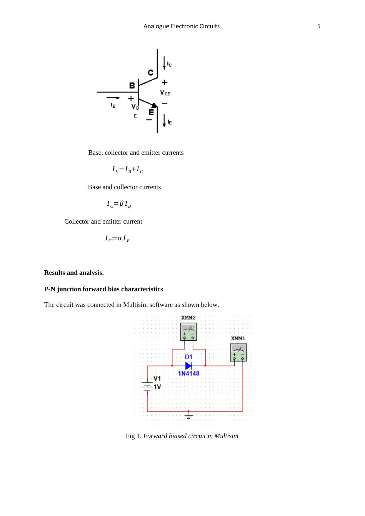
Current relationships of a BJT are as shown by the equation below.
Paraphrase This Document
Need a fresh take? Get an instant paraphrase of this document with our AI Paraphraser
Analogue Electronic Circuits 5
Base, collector and emitter currents
I E =I B +IC
Base and collector currents
I C=β I B
Collector and emitter current
IC=α I E
Results and analysis.
P-N junction forward bias characteristics
The circuit was connected in Multisim software as shown below.
Fig 1. Forward biased circuit in Multisim
Base, collector and emitter currents
I E =I B +IC
Base and collector currents
I C=β I B
Collector and emitter current
IC=α I E
Results and analysis.
P-N junction forward bias characteristics
The circuit was connected in Multisim software as shown below.
Fig 1. Forward biased circuit in Multisim
Analogue Electronic Circuits 6
Adjusting V1 in steps shown in table 1, values of Vd and Id were measured and recorded in the table
below.
Table 1: Diode Voltage and Current.
V1 (V) Vd (V) Id (A)
0.1 100 mV 104.8pA
0.2 200 mV 428.3 pA
0.3 300 mV 11.2 nA
0.4 400 mV 521.0nA
0.5 500 mV 24.8 μA
0.6 600 mV 1.1 mA
0.7 700 mV 18.3 mA
0.8 800 mV 61.3 mA
0.9 900 mV 113.8 mA
1 1000 mV 169.8mA
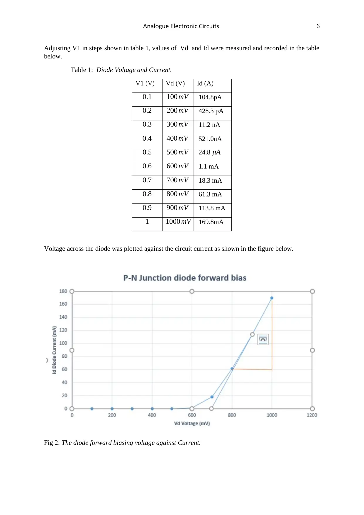
Voltage across the diode was plotted against the circuit current as shown in the figure below.
Fig 2: The diode forward biasing voltage against Current.
⊘ This is a preview!⊘
Do you want full access?
Subscribe today to unlock all pages.

Trusted by 1+ million students worldwide
Analogue Electronic Circuits 7
It was noted that from 0V to 0.6V of the biasing voltage, negligible amount of current in the order of
pA (1 ×10⁻¹²) passed through the diode. Significant amount of current was realized at 0.6V biasing
voltage. The current through the diode increased with increase in biasing voltage. The diode started
behaving ohmic at the biasing voltage beyond 0.7V. Current increased linearly with biasing voltage.
This characteristics is articulated by shrinking of the depletion layer when biasing voltage increases.
As the depletion layer shrinks, potential barrier reduces. The minimum threshold voltage required to
abolish the depletion layer is 0.7V
Forward biased resistance of the diode was found by the expression below;
RD= ∆ V D
∆ I D
= 1−0.8 V
(170−60)× 10−3 =1.82Ω
In summary, the stage when the applied reverse voltage is more than the potential barrier, then the
barrier collapse and many charge carriers are now available making the diode act as a conductor.
P-N junction reverse bias characteristics
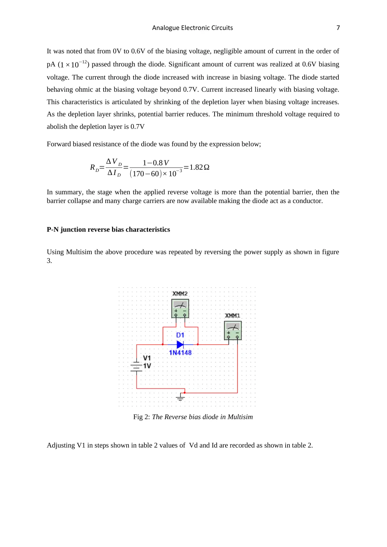
Using Multisim the above procedure was repeated by reversing the power supply as shown in figure
3.
Fig 2: The Reverse bias diode in Multisim
Adjusting V1 in steps shown in table 2 values of Vd and Id are recorded as shown in table 2.
Paraphrase This Document
Need a fresh take? Get an instant paraphrase of this document with our AI Paraphraser
Analogue Electronic Circuits 8
Table 2: Recorded values of Voltage and Current in Reverse diode biasing.
V1 (V) Vd (V) Id (A)
0 0 -0 nA
10 −10 -10.01 nA
20 −20 -20.02 nA
30 −30 -30.03 nA
40 −40 -40.04 nA
50 −50 -50.05 nA
60 −60 -60.06 nA
70 −70 -70.07 nA
80 −80 -80.08 nA
90 −90 -90.09 nA
100 −100 -100.1nA
120 −120 -18.219A
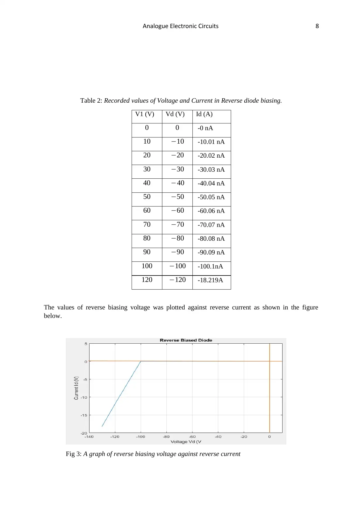
The values of reverse biasing voltage was plotted against reverse current as shown in the figure
below.
Fig 3: A graph of reverse biasing voltage against reverse current
Analogue Electronic Circuits 9
For the values between 0V to 100V (negated because of reverse direction), the diode acted like an
insulator. It only allows infinitesimal amount of reverse current in order of ( 1 ×10⁻⁹ A ) to flow. As
the voltage was increased, there was an outburst of conducting current when reverse biasing voltage
reached 100V. The fact can be explained in terms of expanding potential barrier with increase in
reverse biasing voltage. Potential barrier height increase leads to widening of the depletion layer. This
inhibits movement of majority charge carrier across depletion layer hence acting as an insulator. The
small amount of reverse current is as a contribution of the minority charge carriers across the
depletion layer. When maximum reverse current is exceeded (100V), electrons gain more kinetic
energy to accelerate and knock off silicon bound valences in the depletion layer. This voltage is
known as breakdown voltage.
Diode half wave rectifier
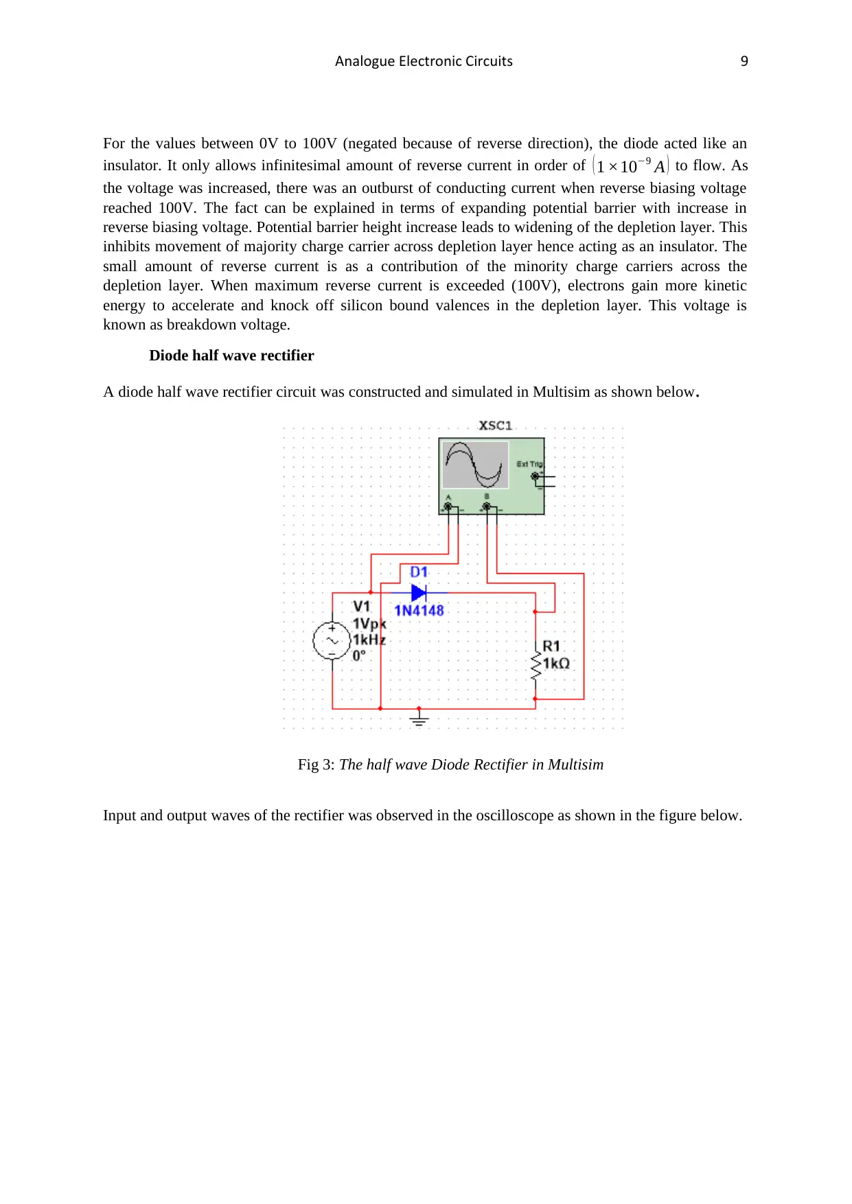
A diode half wave rectifier circuit was constructed and simulated in Multisim as shown below.
Fig 3: The half wave Diode Rectifier in Multisim
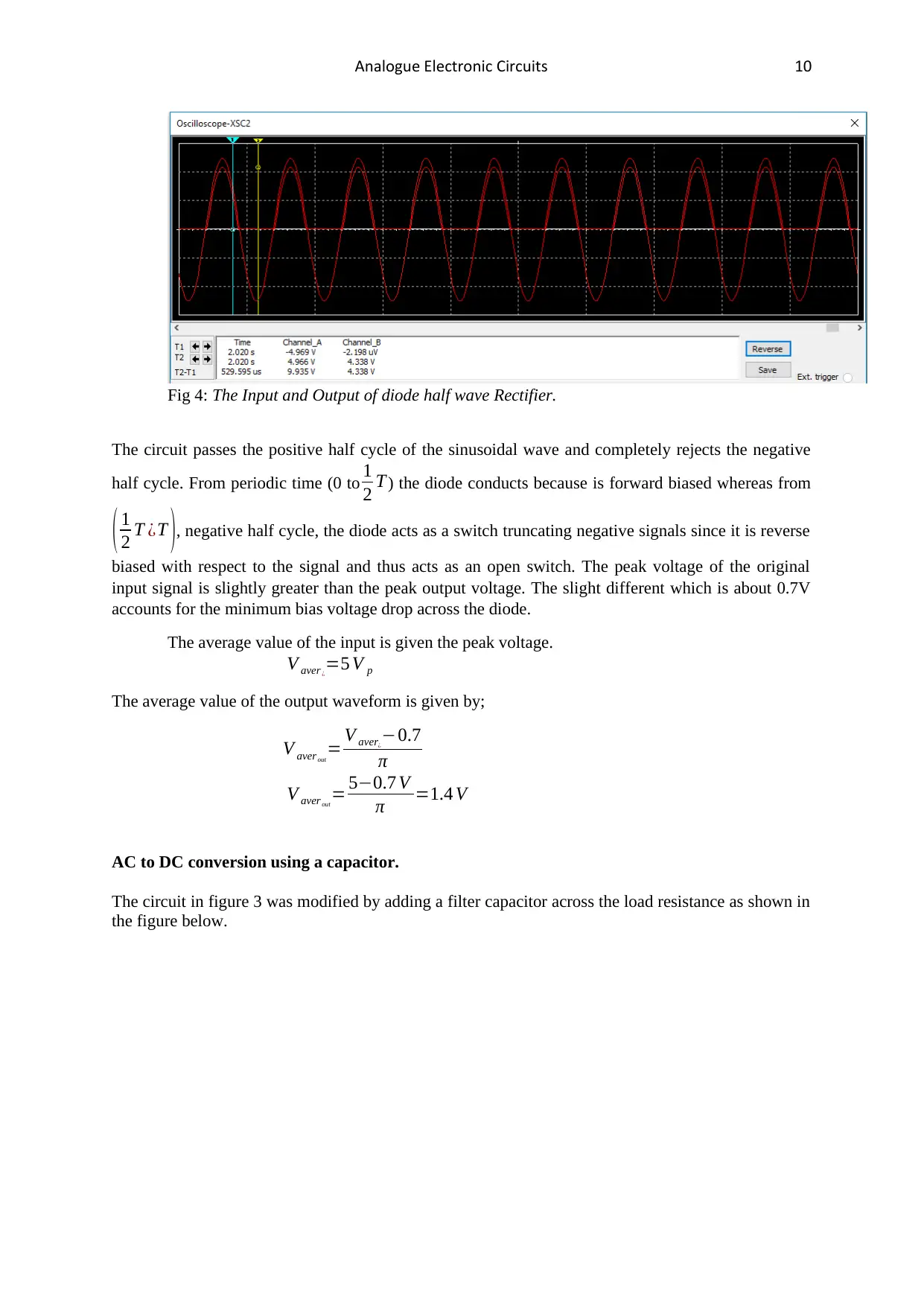
Input and output waves of the rectifier was observed in the oscilloscope as shown in the figure below.
⊘ This is a preview!⊘
Do you want full access?
Subscribe today to unlock all pages.

Trusted by 1+ million students worldwide
Analogue Electronic Circuits 10
Fig 4: The Input and Output of diode half wave Rectifier.
The circuit passes the positive half cycle of the sinusoidal wave and completely rejects the negative
half cycle. From periodic time (0 to 1
2 T ) the diode conducts because is forward biased whereas from
( 1
2 T ¿T ), negative half cycle, the diode acts as a switch truncating negative signals since it is reverse
biased with respect to the signal and thus acts as an open switch. The peak voltage of the original
input signal is slightly greater than the peak output voltage. The slight different which is about 0.7V
accounts for the minimum bias voltage drop across the diode.
The average value of the input is given the peak voltage.
V aver ¿
=5 V p
The average value of the output waveform is given by;
V averout
= V aver¿
−0.7
π
V averout
= 5−0.7 V
π =1.4 V
AC to DC conversion using a capacitor.
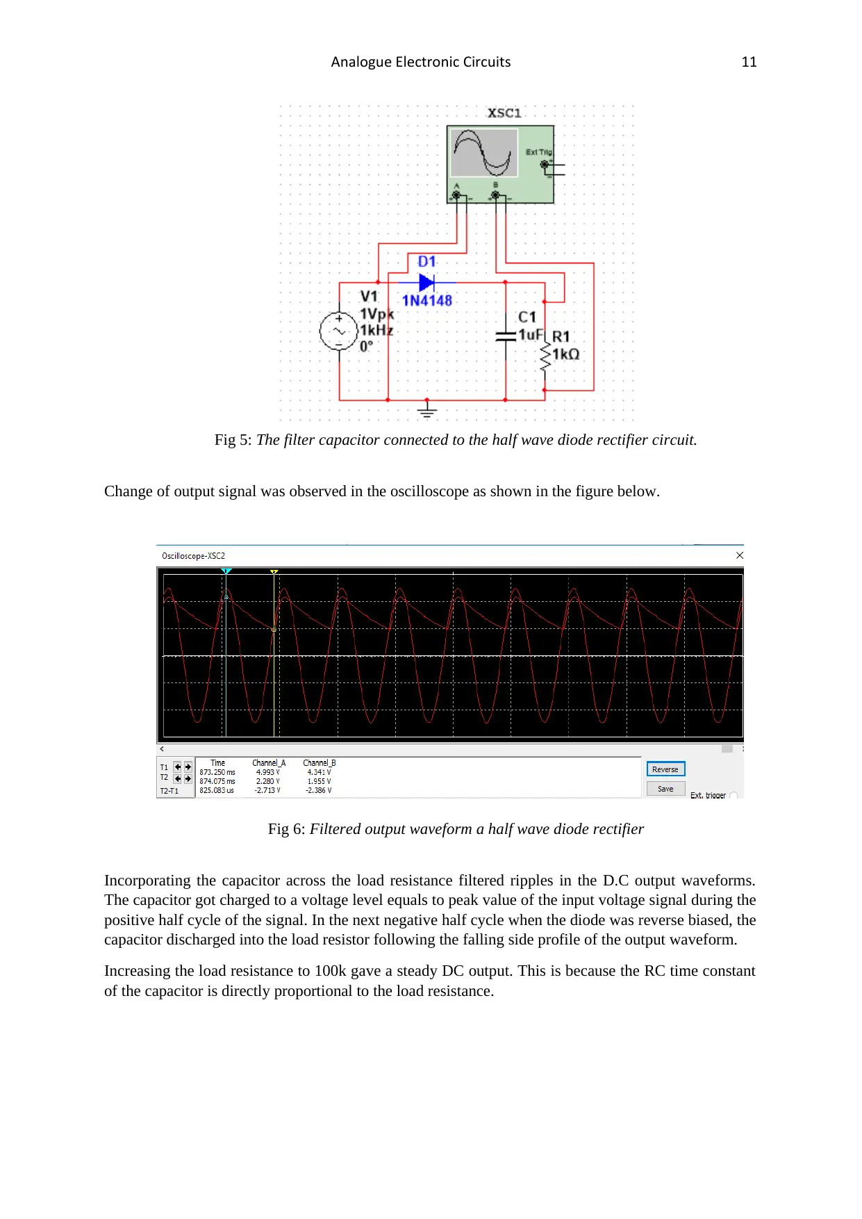
The circuit in figure 3 was modified by adding a filter capacitor across the load resistance as shown in
the figure below.
Paraphrase This Document
Need a fresh take? Get an instant paraphrase of this document with our AI Paraphraser
Analogue Electronic Circuits 11
Fig 5: The filter capacitor connected to the half wave diode rectifier circuit.
Change of output signal was observed in the oscilloscope as shown in the figure below.
Fig 6: Filtered output waveform a half wave diode rectifier
Incorporating the capacitor across the load resistance filtered ripples in the D.C output waveforms.
The capacitor got charged to a voltage level equals to peak value of the input voltage signal during the
positive half cycle of the signal. In the next negative half cycle when the diode was reverse biased, the
capacitor discharged into the load resistor following the falling side profile of the output waveform.
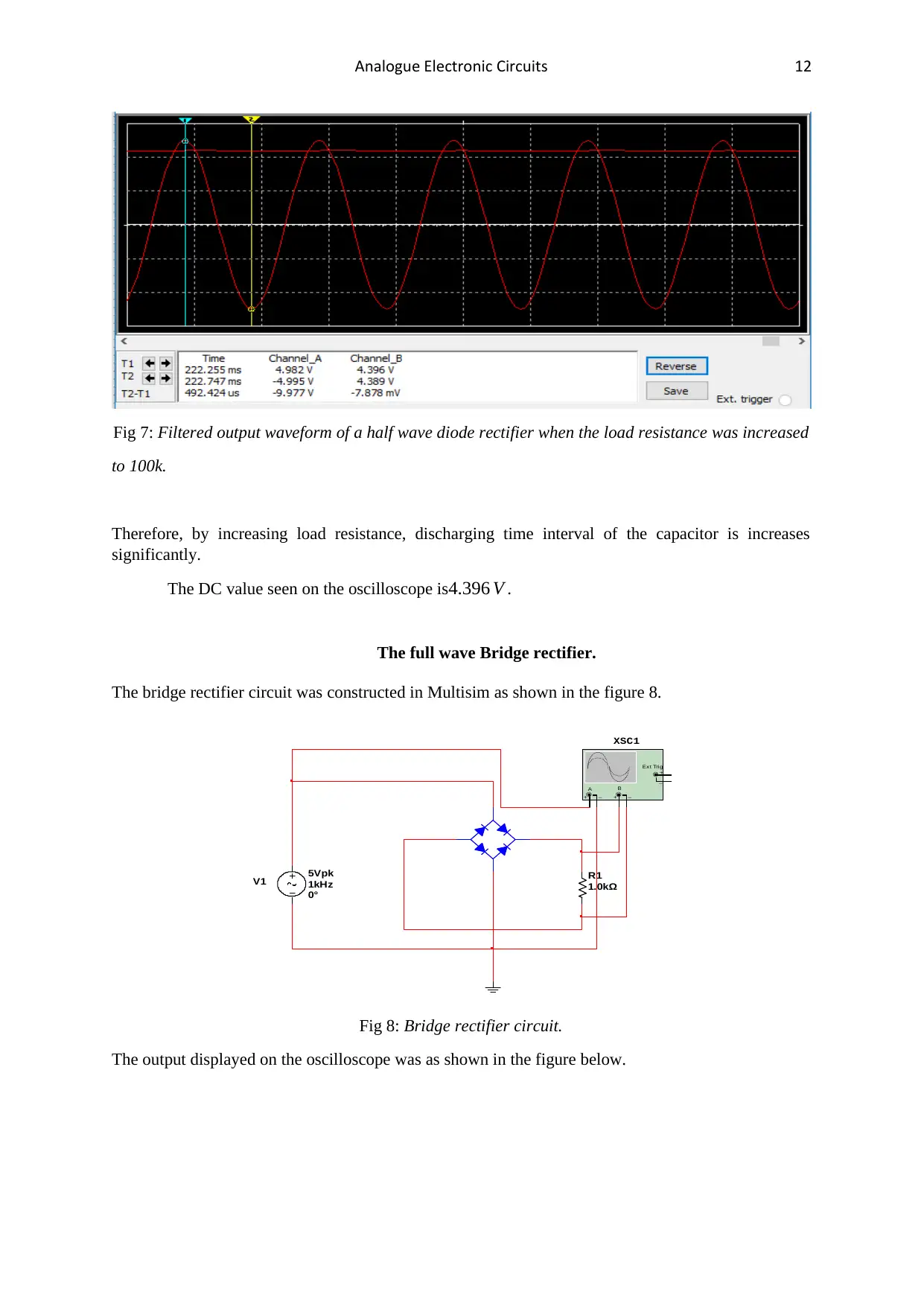
Increasing the load resistance to 100k gave a steady DC output. This is because the RC time constant
of the capacitor is directly proportional to the load resistance.
Analogue Electronic Circuits 12
Fig 7: Filtered output waveform of a half wave diode rectifier when the load resistance was increased
to 100k.
Therefore, by increasing load resistance, discharging time interval of the capacitor is increases
significantly.
The DC value seen on the oscilloscope is 4.396 V .
The full wave Bridge rectifier.
The bridge rectifier circuit was constructed in Multisim as shown in the figure 8.
V1 5Vpk
1kHz
0°
R1
1.0kΩ
XSC1
A B
Ext Trig
+
+
_
_ + _
Fig 8: Bridge rectifier circuit.
The output displayed on the oscilloscope was as shown in the figure below.
⊘ This is a preview!⊘
Do you want full access?
Subscribe today to unlock all pages.

Trusted by 1+ million students worldwide
1 out of 20
Related Documents
Your All-in-One AI-Powered Toolkit for Academic Success.
+13062052269
info@desklib.com
Available 24*7 on WhatsApp / Email
![[object Object]](/_next/static/media/star-bottom.7253800d.svg)
Unlock your academic potential
Copyright © 2020–2026 A2Z Services. All Rights Reserved. Developed and managed by ZUCOL.


