University Circuits Lab: Passive Frequency Selective Circuit Portfolio

Verified

Added on  2022/08/25

|16
|912
|15
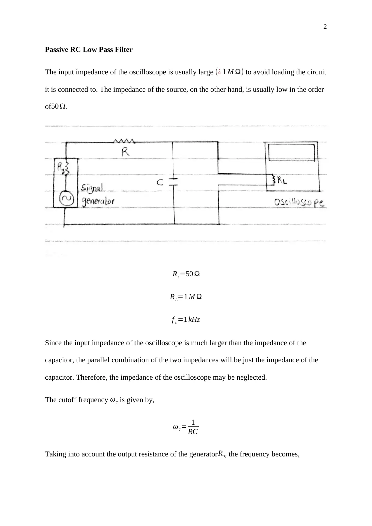
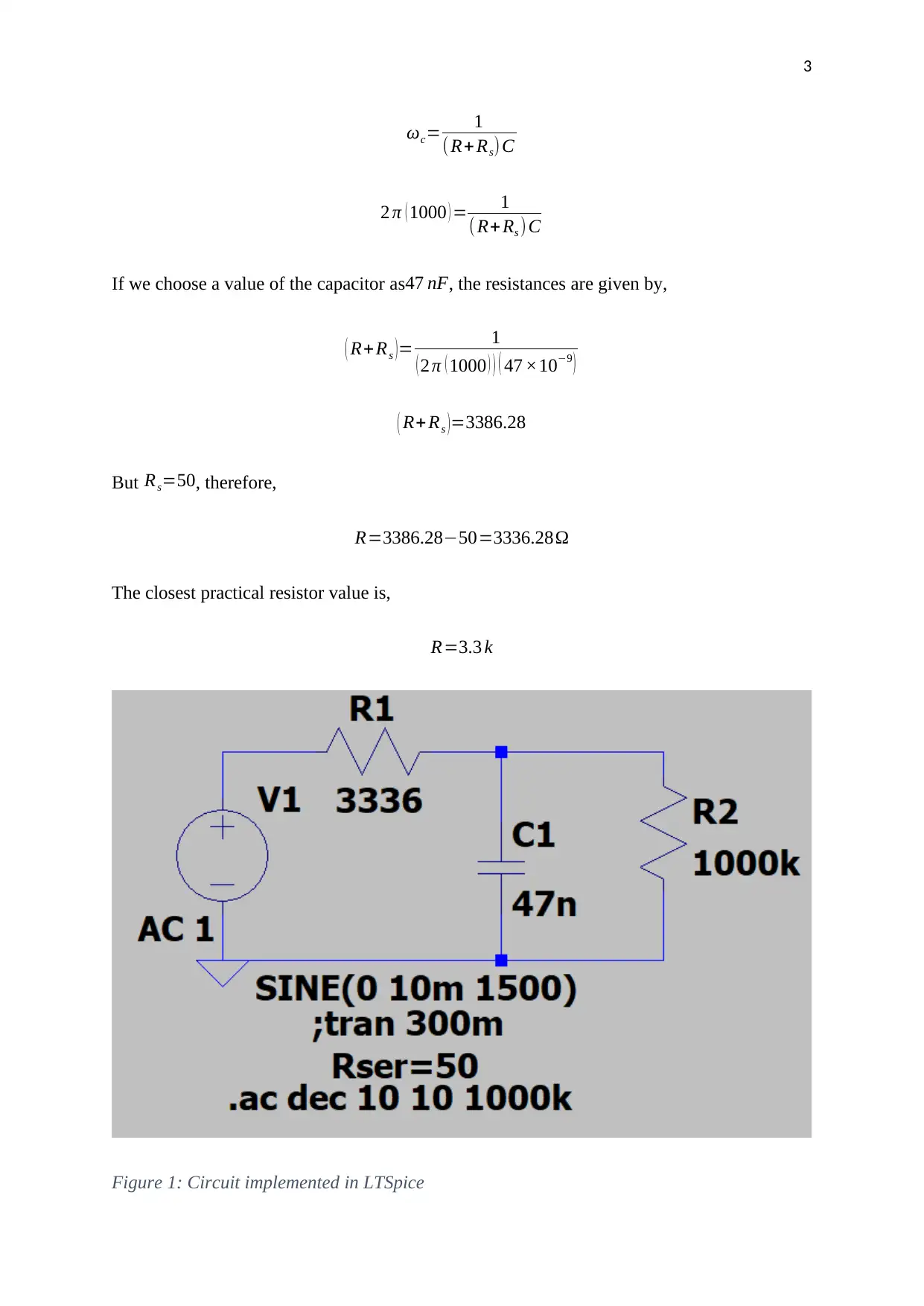
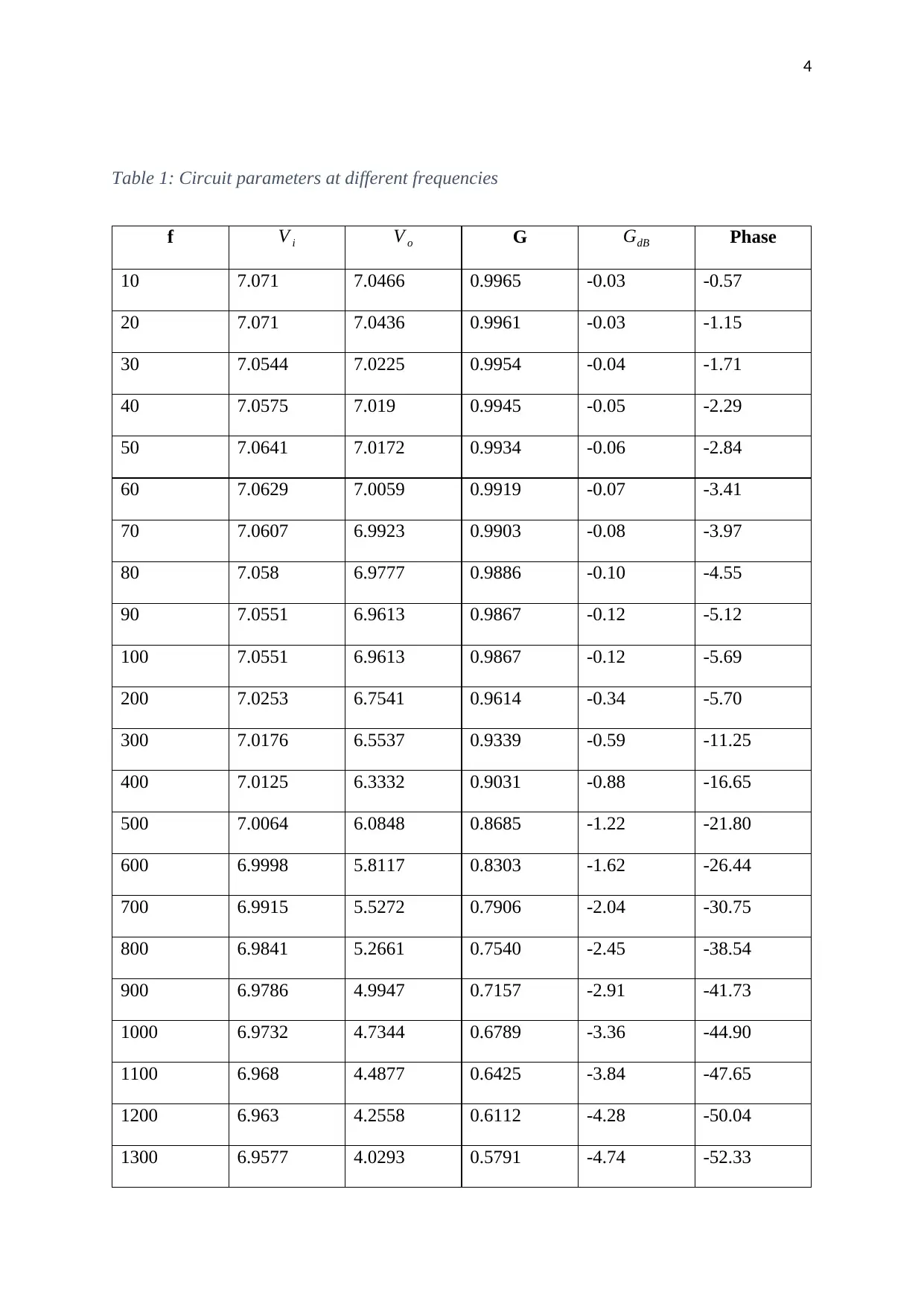
Practical Assignment
AI Summary
This document presents a solution for a practical assignment focused on the analysis and design of passive frequency selective circuits, specifically RC and LC low-pass filters. The assignment involves deriving the two-port network representation of these circuits, calculating key parameters such as cutoff frequency, and analyzing their behavior at different frequencies. The solution includes circuit diagrams implemented in LTSpice, along with tables of circuit parameters and magnitude/phase plots. The student derives transfer functions, calculates slopes, and determines fractional percentage errors. The document also includes discussions on the simulation parameters and their deviations from calculated values, providing a comprehensive overview of the filter design and analysis process. The assignment assesses the students' ability to apply theoretical knowledge to practical circuit design problems.
Document Page
1
Passive Frequency Selective Circuits
Student’s Name
Institutional Affiliation
Date
tabler-icon-diamond-filled.svg

Secure Best Marks with AI Grader

Need help grading? Try our AI Grader for instant feedback on your assignments.
Document Page
2
Passive RC Low Pass Filter
The input impedance of the oscilloscope is usually large (¿ 1 M Ω) to avoid loading the circuit
it is connected to. The impedance of the source, on the other hand, is usually low in the order
of50 Ω.
Rs=50 Ω
RL=1 M Ω
f c=1 kHz
Since the input impedance of the oscilloscope is much larger than the impedance of the
capacitor, the parallel combination of the two impedances will be just the impedance of the
capacitor. Therefore, the impedance of the oscilloscope may be neglected.
The cutoff frequency ωc is given by,
ωc= 1
RC
Taking into account the output resistance of the generatorRs, the frequency becomes,
Document Page
3
ωc= 1
( R+ Rs) C
2 π ( 1000 ) = 1
( R+ Rs ) C
If we choose a value of the capacitor as47 nF, the resistances are given by,
( R+Rs )= 1
( 2 π ( 1000 ) ) ( 47 ×109 )
( R+ Rs )=3386.28
But Rs=50, therefore,
R=3386.2850=3336.28Ω
The closest practical resistor value is,
R=3.3 k
Figure 1: Circuit implemented in LTSpice
Document Page
4
Table 1: Circuit parameters at different frequencies
f V i V o G GdB Phase
10 7.071 7.0466 0.9965 -0.03 -0.57
20 7.071 7.0436 0.9961 -0.03 -1.15
30 7.0544 7.0225 0.9954 -0.04 -1.71
40 7.0575 7.019 0.9945 -0.05 -2.29
50 7.0641 7.0172 0.9934 -0.06 -2.84
60 7.0629 7.0059 0.9919 -0.07 -3.41
70 7.0607 6.9923 0.9903 -0.08 -3.97
80 7.058 6.9777 0.9886 -0.10 -4.55
90 7.0551 6.9613 0.9867 -0.12 -5.12
100 7.0551 6.9613 0.9867 -0.12 -5.69
200 7.0253 6.7541 0.9614 -0.34 -5.70
300 7.0176 6.5537 0.9339 -0.59 -11.25
400 7.0125 6.3332 0.9031 -0.88 -16.65
500 7.0064 6.0848 0.8685 -1.22 -21.80
600 6.9998 5.8117 0.8303 -1.62 -26.44
700 6.9915 5.5272 0.7906 -2.04 -30.75
800 6.9841 5.2661 0.7540 -2.45 -38.54
900 6.9786 4.9947 0.7157 -2.91 -41.73
1000 6.9732 4.7344 0.6789 -3.36 -44.90
1100 6.968 4.4877 0.6425 -3.84 -47.65
1200 6.963 4.2558 0.6112 -4.28 -50.04
1300 6.9577 4.0293 0.5791 -4.74 -52.33
tabler-icon-diamond-filled.svg

Secure Best Marks with AI Grader

Need help grading? Try our AI Grader for instant feedback on your assignments.
Document Page
5
1400 6.9523 3.8057 0.5474 -5.23 -54.21
1500 6.9489 3.6166 0.5205 -5.67 -56.22
Figure 2: The magnitude plot
Figure 3: The phase plot
The cut-off frequency is,
Document Page
6
f c
actual=996.35 Hz
The per decade slope of the magnitude curve is,
Sdecade
actual =19.94 dB/decade
The per octave slope of the magnitude curve is,
Soctave
actual =5.99 dB/octave
The passband phase is,
θpass
actual=ranges ¿ 0 ¿ about44.15 °
Document Page
7
The stopband phase is,
θstop
actual=ranges ¿44.15 °¿ about 89.9°
The phase at the cutoff frequency is,
θactual
cutoff =44.15°
The fractional percentage error between the cutoff frequency value and the one specified in
the design is,
Ef = 1000996.35
1000 ×100 %=0.365 %
Deriving the transfer function for the circuit,
The reactance of the capacitor is,
X c= jωC = 1
jωC
The capacitor is in parallel with the load RL
RL/¿ 1
jωC =
RL × 1
jωC
RL+ 1
jωC
=
RL
jωC
jωC RL+ 1
jωC
= RL
jωC RL+1
Since the output voltage is obtained across the parallel combination of the capacitor and the
load resistor, the transfer function is given by,
H ( ) =
RL /¿ 1
jωC
RL/¿ 1
jωC +R+ Rs
=
RL /¿ 1
jωC
RL/¿ 1
jωC + Re
, w h ere Re=R + Rs
tabler-icon-diamond-filled.svg

Paraphrase This Document

Need a fresh take? Get an instant paraphrase of this document with our AI Paraphraser
Document Page
8
H ( ) =
RL
jωC RL+1
RL
jωC RL+1 +Re
=
RL
jωC RL+1
Re ( jωC RL +1 ) +RL
jωC RL+1
= RL
Re ( jωC RL+1 ) + RL
H ( )= RL
( R+ Rs ) ( jωC RL+1 ) + RL
Two-port network
V 1=Za I1 +Zb I1+ Zc I 1
Z11= V 1
I 1
=Za + Zb +Zc=Rs + R+ jωC
V 2=Zd I2 + Zc I 2
Z22= V 2
I1
=Zd +Zc=RL+ jωC
Z12=Zc=Z21= jωC
6 Passive LC Low Pass Filter
The circuit diagram is shown below,
The cutoff frequency is given by,
Document Page
9
f c= 1
π LC
f c
2= 1
( π ) 2 LC
( πf )2= 1
LC
L= 1
( πf ) 2 C
Let C=1 μF
L= 1
(π2 )(10002 )(1×10⁶ )
¿ 0.1013 H
L=101.3 mH
L
2 =50.65 mH
The available practical component values are,
L=51 mH
C=1 μF
Matching the filter
Z0=π f c LZ0 = 1
π f c C
Z0= ( π ) ( 1000 ) ( 50.65 ) =159.12Ω
The matching load resistance is therefore 159.12Ω
The matching input impedance becomes,
Document Page
10
159.12Rs=159.1250=109.12Ω
Closest actual resistor values are,
R=100Ω
R=150Ω
Figure 4: Circuit implemented in LTSpice
Table 2: Circuit parameters at different frequencies
f V i V o G GdB Phase
10 5.953 3.5273 0.5925 -4.55 -1.43
20 5.9546 3.5168 0.5906 -4.57 -2.85
30 5.9493 3.4979 0.5880 -4.61 -4.31
40 5.944 3.4776 0.5851 -4.66 -5.72
50 5.9424 3.4612 0.5825 -4.69 -7.11
60 5.9423 3.4465 0.5800 -4.73 -8.55
tabler-icon-diamond-filled.svg

Secure Best Marks with AI Grader

Need help grading? Try our AI Grader for instant feedback on your assignments.
Document Page
11
70 5.946 3.4357 0.5778 -4.76 -9.95
80 5.952 3.43 0.5763 -4.79 -11.33
90 5.9605 3.425 0.5746 -4.81 -12.75
100 5.9679 3.4165 0.5725 -4.84 -14.20
200 6.0773 3.311 0.5448 -5.28 -27.88
300 6.2017 3.1835 0.5133 -5.79 -40.42
400 6.3096 3.0878 0.4894 -6.21 -52.03
500 6.372 3.0307 0.4756 -6.45 -63.76
600 6.3801 3.0998 0.4859 -6.27 -75.36
700 6.3005 3.2426 0.5147 -5.77 -89.72
800 6.1025 3.3983 0.5569 -5.08 -107.16
900 5.8323 3.4369 0.5893 -4.59 -129.02
1000 5.7318 3.0784 0.5371 -5.40 -153.41
1100 5.9562 2.4083 0.4043 -7.87 -172.47
1200 6.2425 1.7592 0.2818 -11 -191.05
1300 6.4575 1.2851 0.1990 -14.02 -204.16
1400 6.5987 0.959 0.1453 -16.75 -211.63
1500 6.6923 0.732 0.1094 -19.22 -218.50
Document Page
12
Figure 5: Magnitude plot
Figure 6: Phase plot
The cut-off frequency is,
f c
actual=1.1044 kHz
The per decade slope of the magnitude curve is,
Document Page
13
Sdecade
actual =60.064 dB /decade
The per octave slope of the magnitude curve is,
Soctave
actual =18.105 dB/ octave
The passband phase is,
θpass
actual=0 ¿ about 172.66 °
The stopband phase is,
θstop
actual=269.9 °
tabler-icon-diamond-filled.svg

Paraphrase This Document

Need a fresh take? Get an instant paraphrase of this document with our AI Paraphraser
Document Page
14
The phase at the cutoff frequency is,
θactual
cutoff =172.66 °
The fractional percentage error between the cutoff frequency value and the one specified in
the design is,
Ef = 1.10441
1 ×100 %=10.44 %
Deriving the transfer function
The voltage across the capacitor is found as follows,
V c=
1
jωC
1
jωC + Rm 1 + Rs + jωL1
=
1
jωC
( jωC ) ( jωL1 ) + jωC Rm 1+ jωC Rs +1
jωC
V c= 1
( jωC ) ( jωL1 ) + jωC Rm 1 + jωC Rs +1 = 1
ω2 C L1+ jωC Rm 1 + jωC Rs+ 1 V i
The parallel combination of RL and the second matching resistor Rm 2 is,
RL/¿ Rm 2= RL Rm 2
RL+ Rm 2
The output voltage is obtained across this parallel combination,
V o =
RL Rm 2
RL+ Rm 2
RL Rm2
RL+ Rm 2
+ jωL2
V c
V o =
RL Rm 2
RL + Rm 2
jωL2 (R¿¿ L+Rm 2 )+ RL Rm 2
RL+ Rm 2
V c ¿
Document Page
15
V o = RL Rm 2
jωL2 (R¿ ¿ L+ Rm 2)+ RL Rm 2 × 1
ω2 C L1+ jωC Rm 1 + jωC Rs+ 1 V i ¿
V o
V i
=H ( ω ) = RL Rm 2
¿ ¿
Two-port network
V 1=Za I 1 +Zb I 1+Zc I 1+Zd I 1
V 1
I1
=Z11=Za + Zb +Zc + Zd=Rs + Rm 1 + L1+ jωC
V 1
I2
=Z12=Zd = jωC
V 2=Zd I2 + Ze I 2+ Zf × Zg
Zf + Zg
I2
V 2
I2
=Zd + Ze+ Zf × Zg
Zf + Zg
=RL/¿ Rm 1 + L2+ jωC
V 2
I1
=Z21=Zd = jωC
Conclusions
The simulation parameters show some deviation from the calculated values. This may be
attributed to the fact that the calculated parameters are an estimation due to round-off errors.
For instance, the cut-off frequency is an estimated value hence when it is obtained from the
magnitude plot, its value is slightly different from the calculated value. In practice, the
difference between the calculated values and the values from actual measurements using an
oscilloscope would be larger due to the use of non-ideal devices with certain tolerances. The
Document Page
16
two transfer functions have a different number of poles. The RC network has a single-pole
since it has only one frequency-dependent element. Its roll-off rate is 20 dB /decade as
expected. The LC network, on the other hand, has 3 frequency selective components (2
inductors and a capacitor). Therefore, it has 3 poles and the roll-off rate is 60 dB / decade as
expected.
chevron_up_icon
1 out of 16
circle_padding
hide_on_mobile
zoom_out_icon
[object Object]