In-Depth Analysis of Computer Systems Architecture Principles
VerifiedAdded on 2024/04/24
|35
|6207
|361
Report
AI Summary
This report provides a comprehensive overview of computer systems architecture, dividing the subject into three main parts. The first section details number systems and their representation within computer systems, including data conversion into binary format for various data types like music, video, and images, along with explanations of number system conversions and logic gates. The second part explores the Von-Neumann architecture, its components, memory types, and communication methods using polling and interrupts. Finally, the report compares Reduced Instruction Set Computer (RISC) and Complex Instruction Set Computer (CISC) architectures and elucidates the fetch-execute cycle with its associated processor registers. This document is available on Desklib, a platform offering a wide range of study tools and solved assignments for students.
Computer Systems Architecture
0
0
Paraphrase This Document
Need a fresh take? Get an instant paraphrase of this document with our AI Paraphraser
Table of Contents
Introduction................................................................................................................................4
LO1 Understand how data can be represented within computer systems..................................5
P1. Explain using examples how numeric and alphanumeric data can be coded within a
computer system.....................................................................................................................5
P2. Explain using examples how different types of data can be converted and stored in
computer system.....................................................................................................................8
P3. Convert numeric data between different number systems including floating point......10
P4. Carry out Boolean logic operations...............................................................................13
LO2 Understand the functions of computer system components............................................17
P5 illustrate the key computer system components and how they interact..........................17
P6 explain the different types of memory that can be attached to a processor....................20
P7 explain how polling and interrupts are used to allow communication between processor
and peripherals.....................................................................................................................24
LO3 Understand the principles of processor operations..........................................................27
P8 compare Reduced Instruction Set Computer (RISC) chips and Complex Instruction Set
Computer (CISC) chips........................................................................................................27
P9 illustrate the use of the different processor registers in the fetch-execute cycle............30
Conclusion................................................................................................................................32
References:...............................................................................................................................33
1
List of Figure
Figure 1: ASCII code table........................................................................................................6
Figure 2: Binary represent of image...........................................................................................8
Figure 3: sound represent in binary format................................................................................9
Figure 4: Logical diagram of AND Gate.................................................................................13
Figure 5: Logical diagram of OR Gate....................................................................................14
Figure 6: Logical diagram of NOT Gate..................................................................................14
Figure 7: Logical diagram of NAND Gate..............................................................................15
Figure 8: Logical diagram of NOR Gate..................................................................................15
Figure 9: Logical diagram of EXOR Gate...............................................................................15
Figure 10: Logical diagram of ENXOR Gate..........................................................................16
Figure 11: Logical diagram......................................................................................................16
Figure 12: Von-Neumann Architecture...................................................................................17
Figure 13: Keyboard................................................................................................................17
Figure 14: Mouse.....................................................................................................................18
Figure 15: Printer.....................................................................................................................18
Figure 16: Monitor...................................................................................................................18
Figure 17: ALU structure.........................................................................................................19
Figure 18: Memory unit in computer.......................................................................................20
Figure 19: Computer hard drive...............................................................................................22
Figure 20: Pen Drive................................................................................................................22
Figure 21: Interrupt process in system.....................................................................................24
Figure 22: Polling process in System......................................................................................25
Figure 23: RISC Architecture..................................................................................................27
Figure 24: CICS Architecture..................................................................................................28
Figure 25: Difference between RICS and CISC working........................................................29
Figure 26: Fetch-execute cycle in Processor register...............................................................30
2
⊘ This is a preview!⊘
Do you want full access?
Subscribe today to unlock all pages.
Trusted by 1+ million students worldwide
List of Table:
Table 1: Conversion table of number system.............................................................................5
Table 2: Binary Number system for decimal number................................................................7
Table 3: Truth table of AND gate............................................................................................13
Table 4: Truth Table of OR Gate.............................................................................................14
Table 5: Truth Table of Not Gate.............................................................................................14
Table 6: Truth table of NAND Gate........................................................................................14
Table 7: Truth Table of NOR Gate..........................................................................................15
Table 8: Truth table of EXOR Gate.........................................................................................15
Table 9: Truth table of ENXOR Gate......................................................................................16
Table 10: Truth table of given logical diagram........................................................................16
Table 12: Compression between interrupts and polling...........................................................25
Table 13: Comparison Table between RISC and CISC...........................................................28
3
Paraphrase This Document
Need a fresh take? Get an instant paraphrase of this document with our AI Paraphraser
Introduction
The computer system is a complex system which contains various sub-systems. Each sub-
system is a part of computer hardware. System parts interact is called the "Computer
Architecture".
Report of Computer Architecture is divided into three parts. The first part, it is described
number system and their representation in the computer system. Future, this part is given
detail about Data (like music, video, image, audios) conversion into binary format and how to
store into the computer system. It also explains number system conversion one format to
other format and logical gate with the truth table.
The second part, it is explained system Von-Neumann architecture with its components,
Memory which is used by system and polling or interrupts which is used for sharing
information.
The third part, it is described the comparison between RISC and CISC and the end of the
report explain fetch-execute cycles and the steps.
4
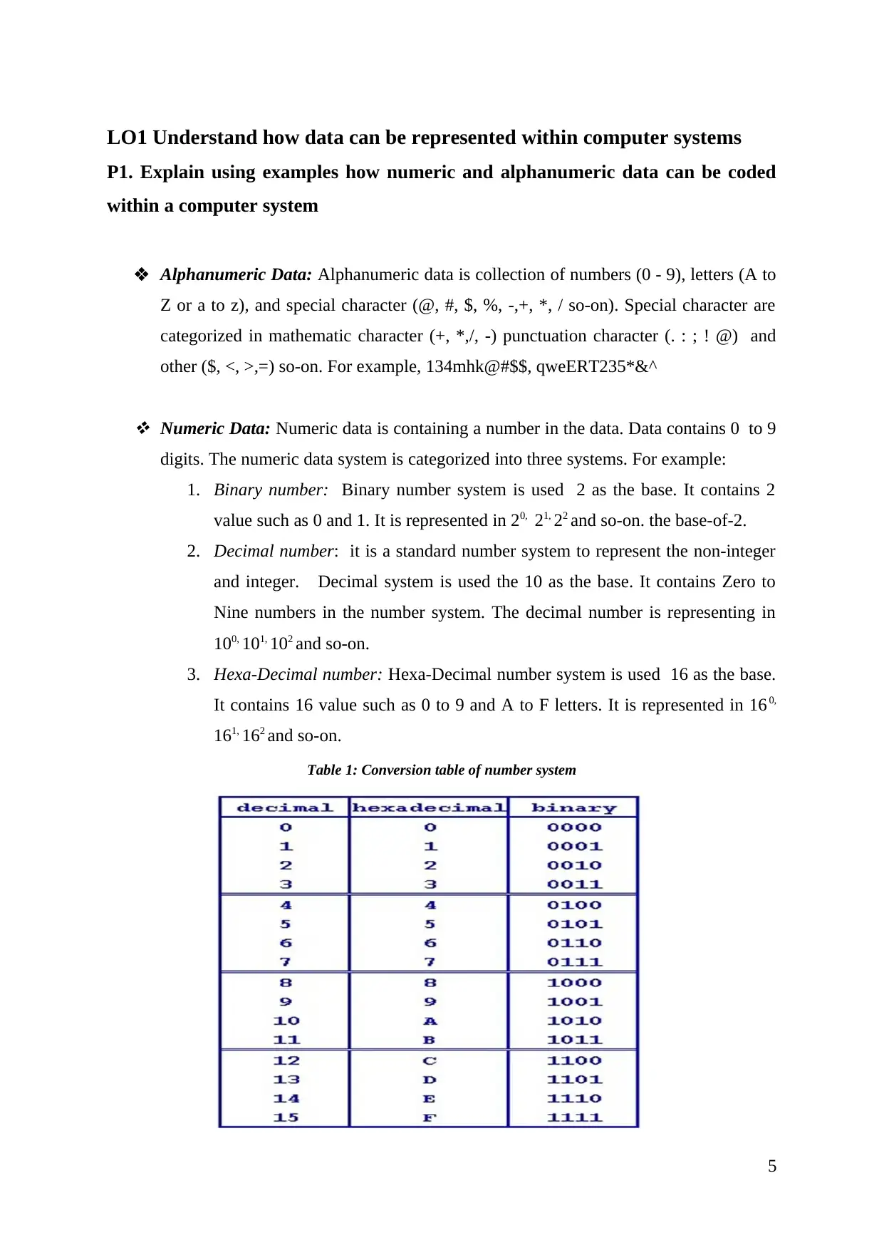
LO1 Understand how data can be represented within computer systems
P1. Explain using examples how numeric and alphanumeric data can be coded
within a computer system
Alphanumeric Data: Alphanumeric data is collection of numbers (0 - 9), letters (A to
Z or a to z), and special character (@, #, $, %, -,+, *, / so-on). Special character are
categorized in mathematic character (+, *,/, -) punctuation character (. : ; ! @) and
other ($, <, >,=) so-on. For example, 134mhk@#$$, qweERT235*&^
Numeric Data: Numeric data is containing a number in the data. Data contains 0 to 9
digits. The numeric data system is categorized into three systems. For example:
1. Binary number: Binary number system is used 2 as the base. It contains 2
value such as 0 and 1. It is represented in 20, 21, 22 and so-on. the base-of-2.
2. Decimal number: it is a standard number system to represent the non-integer
and integer. Decimal system is used the 10 as the base. It contains Zero to
Nine numbers in the number system. The decimal number is representing in
100, 101, 102 and so-on.
3. Hexa-Decimal number: Hexa-Decimal number system is used 16 as the base.
It contains 16 value such as 0 to 9 and A to F letters. It is represented in 16 0,
161, 162 and so-on.
Table 1: Conversion table of number system
5
⊘ This is a preview!⊘
Do you want full access?
Subscribe today to unlock all pages.
Trusted by 1+ million students worldwide
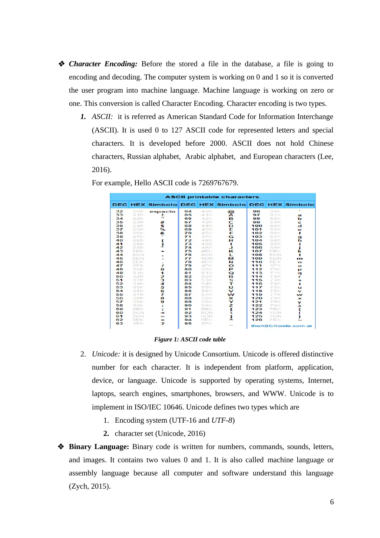
Character Encoding: Before the stored a file in the database, a file is going to
encoding and decoding. The computer system is working on 0 and 1 so it is converted
the user program into machine language. Machine language is working on zero or
one. This conversion is called Character Encoding. Character encoding is two types.
1. ASCII: it is referred as American Standard Code for Information Interchange
(ASCII). It is used 0 to 127 ASCII code for represented letters and special
characters. It is developed before 2000. ASCII does not hold Chinese
characters, Russian alphabet, Arabic alphabet, and European characters (Lee,
2016).
For example, Hello ASCII code is 7269767679.
Figure 1: ASCII code table
2. Unicode: it is designed by Unicode Consortium. Unicode is offered distinctive
number for each character. It is independent from platform, application,
device, or language. Unicode is supported by operating systems, Internet,
laptops, search engines, smartphones, browsers, and WWW. Unicode is to
implement in ISO/IEC 10646. Unicode defines two types which are
1. Encoding system (UTF-16 and UTF-8)
2. character set (Unicode, 2016)
Binary Language: Binary code is written for numbers, commands, sounds, letters,
and images. It contains two values 0 and 1. It is also called machine language or
assembly language because all computer and software understand this language
(Zych, 2015).
6
Paraphrase This Document
Need a fresh take? Get an instant paraphrase of this document with our AI Paraphraser
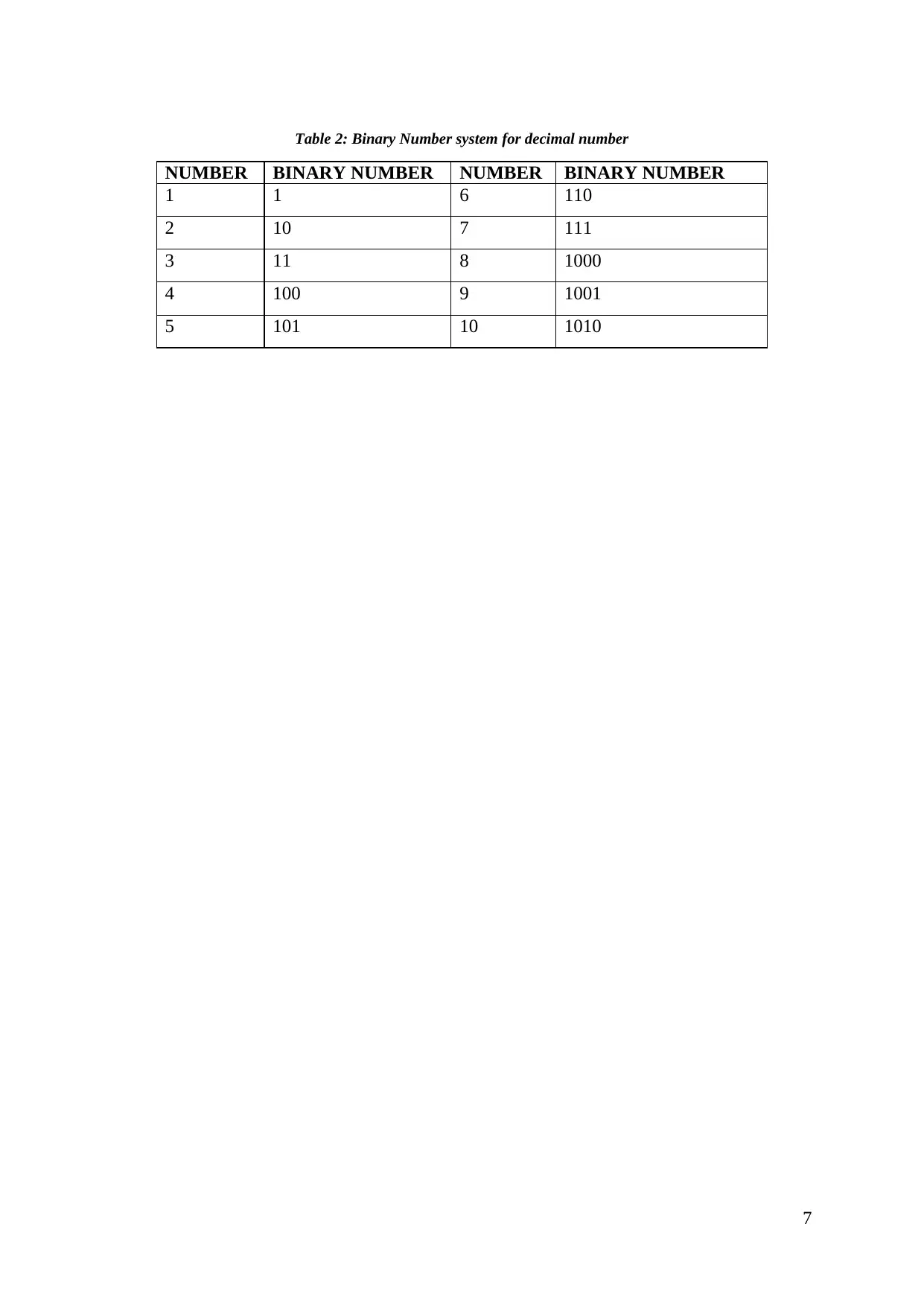
Table 2: Binary Number system for decimal number
7
NUMBER BINARY NUMBER NUMBER BINARY NUMBER
1 1 6 110
2 10 7 111
3 11 8 1000
4 100 9 1001
5 101 10 1010
7
NUMBER BINARY NUMBER NUMBER BINARY NUMBER
1 1 6 110
2 10 7 111
3 11 8 1000
4 100 9 1001
5 101 10 1010
P2. Explain using examples how different types of data can be converted and
stored in computer system
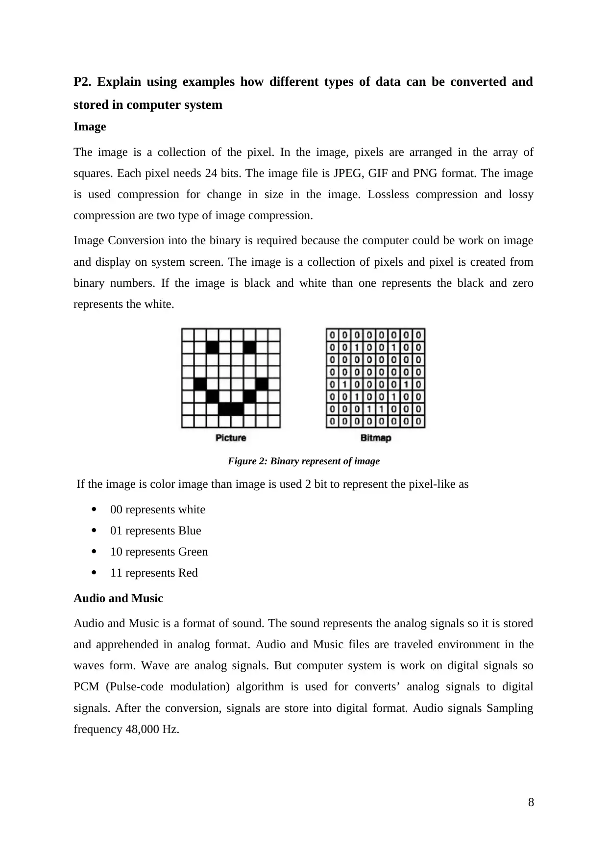
Image
The image is a collection of the pixel. In the image, pixels are arranged in the array of
squares. Each pixel needs 24 bits. The image file is JPEG, GIF and PNG format. The image
is used compression for change in size in the image. Lossless compression and lossy
compression are two type of image compression.
Image Conversion into the binary is required because the computer could be work on image
and display on system screen. The image is a collection of pixels and pixel is created from
binary numbers. If the image is black and white than one represents the black and zero
represents the white.
Figure 2: Binary represent of image
If the image is color image than image is used 2 bit to represent the pixel-like as
00 represents white
01 represents Blue
10 represents Green
11 represents Red
Audio and Music
Audio and Music is a format of sound. The sound represents the analog signals so it is stored
and apprehended in analog format. Audio and Music files are traveled environment in the
waves form. Wave are analog signals. But computer system is work on digital signals so
PCM (Pulse-code modulation) algorithm is used for converts’ analog signals to digital
signals. After the conversion, signals are store into digital format. Audio signals Sampling
frequency 48,000 Hz.
8
stored in computer system
Image
The image is a collection of the pixel. In the image, pixels are arranged in the array of
squares. Each pixel needs 24 bits. The image file is JPEG, GIF and PNG format. The image
is used compression for change in size in the image. Lossless compression and lossy
compression are two type of image compression.
Image Conversion into the binary is required because the computer could be work on image
and display on system screen. The image is a collection of pixels and pixel is created from
binary numbers. If the image is black and white than one represents the black and zero
represents the white.
Figure 2: Binary represent of image
If the image is color image than image is used 2 bit to represent the pixel-like as
00 represents white
01 represents Blue
10 represents Green
11 represents Red
Audio and Music
Audio and Music is a format of sound. The sound represents the analog signals so it is stored
and apprehended in analog format. Audio and Music files are traveled environment in the
waves form. Wave are analog signals. But computer system is work on digital signals so
PCM (Pulse-code modulation) algorithm is used for converts’ analog signals to digital
signals. After the conversion, signals are store into digital format. Audio signals Sampling
frequency 48,000 Hz.
8
⊘ This is a preview!⊘
Do you want full access?
Subscribe today to unlock all pages.
Trusted by 1+ million students worldwide
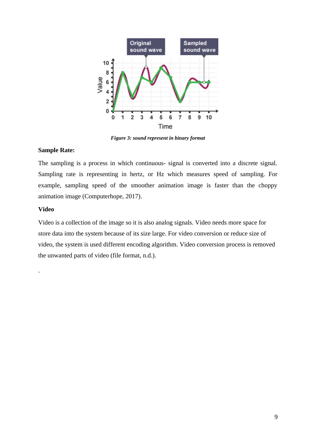
Figure 3: sound represent in binary format
Sample Rate:
The sampling is a process in which continuous- signal is converted into a discrete signal.
Sampling rate is representing in hertz, or Hz which measures speed of sampling. For
example, sampling speed of the smoother animation image is faster than the choppy
animation image (Computerhope, 2017).
Video
Video is a collection of the image so it is also analog signals. Video needs more space for
store data into the system because of its size large. For video conversion or reduce size of
video, the system is used different encoding algorithm. Video conversion process is removed
the unwanted parts of video (file format, n.d.).
.
9
Paraphrase This Document
Need a fresh take? Get an instant paraphrase of this document with our AI Paraphraser
P3. Convert numeric data between different number systems including floating
point
Number System:
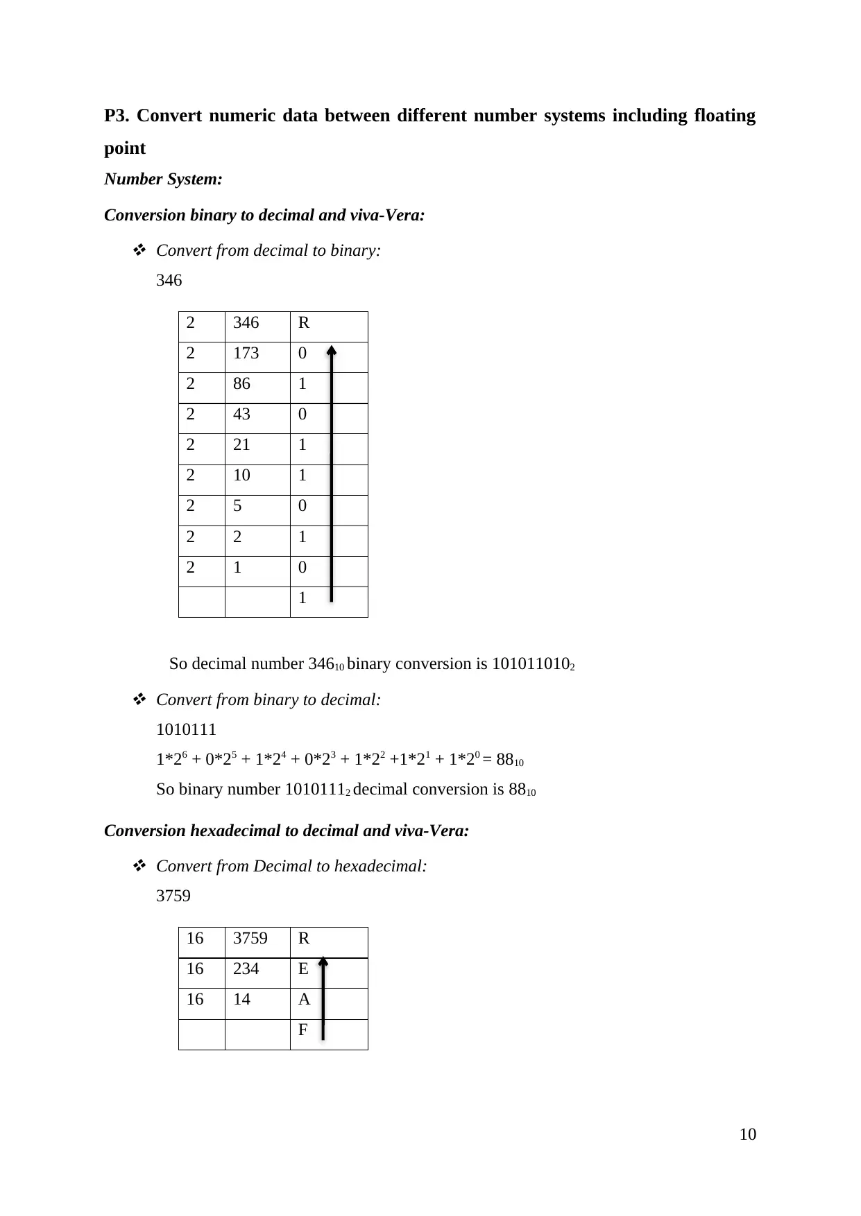
Conversion binary to decimal and viva-Vera: Convert from decimal to binary:
346
2 346 R
2 173 0
2 86 1
2 43 0
2 21 1
2 10 1
2 5 0
2 2 1
2 1 0
1
So decimal number 34610 binary conversion is 1010110102 Convert from binary to decimal:
1010111
1*26 + 0*25 + 1*24 + 0*23 + 1*22 +1*21 + 1*20 = 8810
So binary number 10101112 decimal conversion is 8810
Conversion hexadecimal to decimal and viva-Vera: Convert from Decimal to hexadecimal:
3759
16 3759 R
16 234 E
16 14 A
F
10
point
Number System:
Conversion binary to decimal and viva-Vera: Convert from decimal to binary:
346
2 346 R
2 173 0
2 86 1
2 43 0
2 21 1
2 10 1
2 5 0
2 2 1
2 1 0
1
So decimal number 34610 binary conversion is 1010110102 Convert from binary to decimal:
1010111
1*26 + 0*25 + 1*24 + 0*23 + 1*22 +1*21 + 1*20 = 8810
So binary number 10101112 decimal conversion is 8810
Conversion hexadecimal to decimal and viva-Vera: Convert from Decimal to hexadecimal:
3759
16 3759 R
16 234 E
16 14 A
F
10
So decimal number 375910 binary conversion is EAF16
Convert from Hexadecimal to decimal:
B59F
B*163 + 5*162 +9*161 + F*160 = 4649510
So binary number B59F16 decimal conversion is 4649510
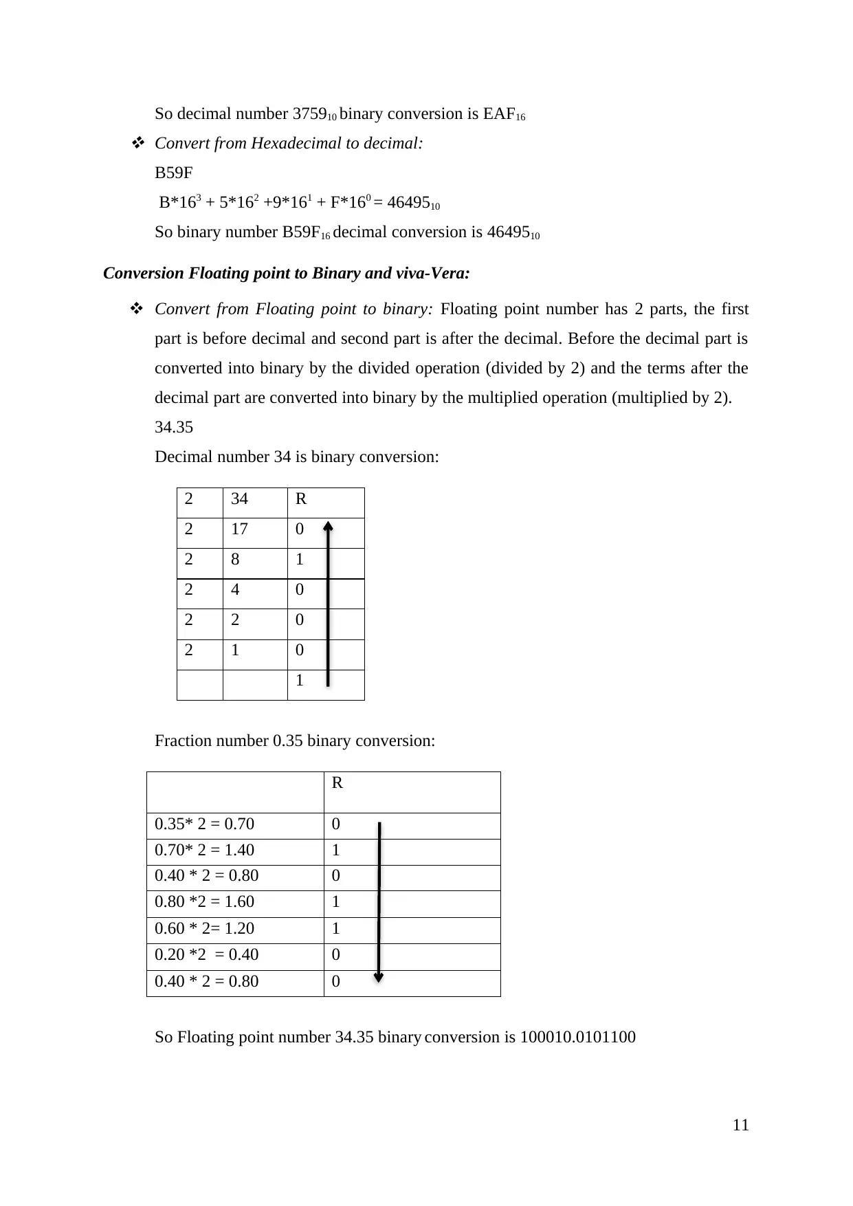
Conversion Floating point to Binary and viva-Vera:
Convert from Floating point to binary: Floating point number has 2 parts, the first
part is before decimal and second part is after the decimal. Before the decimal part is
converted into binary by the divided operation (divided by 2) and the terms after the
decimal part are converted into binary by the multiplied operation (multiplied by 2).
34.35
Decimal number 34 is binary conversion:
2 34 R
2 17 0
2 8 1
2 4 0
2 2 0
2 1 0
1
Fraction number 0.35 binary conversion:
R
0.35* 2 = 0.70 0
0.70* 2 = 1.40 1
0.40 * 2 = 0.80 0
0.80 *2 = 1.60 1
0.60 * 2= 1.20 1
0.20 *2 = 0.40 0
0.40 * 2 = 0.80 0
So Floating point number 34.35 binary conversion is 100010.0101100
11
Convert from Hexadecimal to decimal:
B59F
B*163 + 5*162 +9*161 + F*160 = 4649510
So binary number B59F16 decimal conversion is 4649510
Conversion Floating point to Binary and viva-Vera:
Convert from Floating point to binary: Floating point number has 2 parts, the first
part is before decimal and second part is after the decimal. Before the decimal part is
converted into binary by the divided operation (divided by 2) and the terms after the
decimal part are converted into binary by the multiplied operation (multiplied by 2).
34.35
Decimal number 34 is binary conversion:
2 34 R
2 17 0
2 8 1
2 4 0
2 2 0
2 1 0
1
Fraction number 0.35 binary conversion:
R
0.35* 2 = 0.70 0
0.70* 2 = 1.40 1
0.40 * 2 = 0.80 0
0.80 *2 = 1.60 1
0.60 * 2= 1.20 1
0.20 *2 = 0.40 0
0.40 * 2 = 0.80 0
So Floating point number 34.35 binary conversion is 100010.0101100
11
⊘ This is a preview!⊘
Do you want full access?
Subscribe today to unlock all pages.
Trusted by 1+ million students worldwide
1 out of 35
Related Documents


Your All-in-One AI-Powered Toolkit for Academic Success.
+13062052269
info@desklib.com
Available 24*7 on WhatsApp / Email
![[object Object]](/_next/static/media/star-bottom.7253800d.svg)
Unlock your academic potential
Copyright © 2020–2026 A2Z Services. All Rights Reserved. Developed and managed by ZUCOL.