Plasma Enhanced Chemical Vapor Deposition Reactor Design Project
VerifiedAdded on 2021/04/17
|8
|2019
|81
Project
AI Summary
This project presents a comprehensive exploration of Plasma Enhanced Chemical Vapor Deposition (PECVD) for the growth of carbon nanotubes, focusing on the design of a desktop reactor. The literature review establishes the advantages of PECVD over low-pressure chemical vapor deposition, particularly its lower processing temperatures and suitability for vertical nanotube growth. The project emphasizes the importance of identifying customer and engineering requirements, using a quality function deployment diagram for analysis. The design details the operating conditions, component selection, and design modules, including the reaction chamber, plasma coil, and controllers. The document discusses both local and remote plasma techniques, favoring remote plasma for its weaker electric field. It also covers the electronic components, failure analysis, and potential environmental impacts, providing a complete overview of the reactor design and its practical considerations. The project aims to provide a clear understanding of the system design, analysis, and potential issues that can be encountered during the design process.
Plasma Enhanced Chemical Vapor Deposition 1
PROJECT ON THE CARBON NANOTUBE DESKTOP REACTOR WITH PLASMA
ENHANCED GROWTH
A Research Paper on Plasma By
Student’s Name
Name of the Professor
Institutional Affiliation
City/State
Year/Month/Day
PROJECT ON THE CARBON NANOTUBE DESKTOP REACTOR WITH PLASMA
ENHANCED GROWTH
A Research Paper on Plasma By
Student’s Name
Name of the Professor
Institutional Affiliation
City/State
Year/Month/Day
Paraphrase This Document
Need a fresh take? Get an instant paraphrase of this document with our AI Paraphraser
Plasma Enhanced Chemical Vapor Deposition 2
LITERATURE REVIEW
The plasma enhanced chemical vapour deposition is a technology of chemical vapour
deposition that uses a plasma to give some of the energy for the deposition reaction to be
carried out. This gives a benefit of processing of lower temperature than the use of methods
of purely thermal processing such as low-pressure chemical vapour deposition. The
processing temperatures of plasma enhanced chemical vapour deposition range between
200oC to 400oC while the processing temperatures of the low-pressure chemical vapour
deposition range between 425oC to 900oC. The plasma enhanced chemical vapour deposition
system which is normally abbreviated as PECVD is a type of the chemical vapour deposition
process which normally differs in the means by which the chemical reactions are initiated.
This research seeks to discuss on the addition of plasma into the system so as to make
sure that the growth is vertically explicit since it is difficult to create the vertical nanotubes by
the use of the system of chemical vapour deposition. This project is motivated towards
coming up with enhanced and well-sized system of desktop plasma deposition. For this
design to be effective, there is need for identification of the customer requirements and also
quantitative engineering requirements and the analysis carried out using quality function
deployment diagram (Chopra, 2012). The major requirements are:
Operating contrition controller
Sizable system size that can fit on the desktop easily
A cap that is adjustable that changes the electric field condition (Franssila,
2010)
Operation of PECVD
The dilution and reactant gases flow into process chamber by a shower head which is
a huge metal plate that is perforated and situated above the sample. The shower heat assists in
providing an extra uniform distribution of reactant gas flow over the surface of the sample.
Electrons that are energetic in the plasma dissociate or ionize the reactant gases to produce
Plasma Enhanced Chemical Vapor Deposition 3
extra radicals that are chemically reactive. The radicals react to produce the thin film of
material deposition on the sample's top. The supplied energy by the plasma gives the major
advantage of the minimized temperature of the process for plasma enhanced chemical vapour
deposition compared to low-pressure chemical vapour deposition where every energy for
reaction is thermally supplied (Konuma, 2011).
Methods of Designing PECVD
There are two methods which can be used when designing the plasma enhanced
chemical vapour deposition, these methods include local techniques and remote techniques.
In the remote plasma design, the substrate is developed on a substrate that is separate.
Whereas for the local plasma design system, the plasma is generated directly on the substrate
in the environment provided. In the local plasma. The electric field is developed on the
substrate and the electric field can result in the destruction of the nanotubes. In the remote
plasma, there is no development of the electric field over the substrate and there is weak
electric field produced on the substrate (Mattox, 2016).
From the features above of both the local plasma and the remote plasma, the most
preferred technique is the remote design since there is weaker electric field produced on the
substrate for this particular design. Some of the major components of the system that need to
be developed when designing the plasma enhanced chemical vapor deposition system
including the inductive plasma box, tube with remote inductive plasma and oven heating,
tube with remote inductive plasma and DC substrate bias, steel or pyrex six-way cross with
remote inductive plasma and DC substrate bias, pyrex cross with remote inductive plasma
and DC substrate bias (Ostrikov, 2011).
The vapour deposition system can be categorized into three modules namely
controllers, reaction chamber, and plasma coil. The methods that are normally used in
⊘ This is a preview!⊘
Do you want full access?
Subscribe today to unlock all pages.
Trusted by 1+ million students worldwide
Plasma Enhanced Chemical Vapor Deposition 4
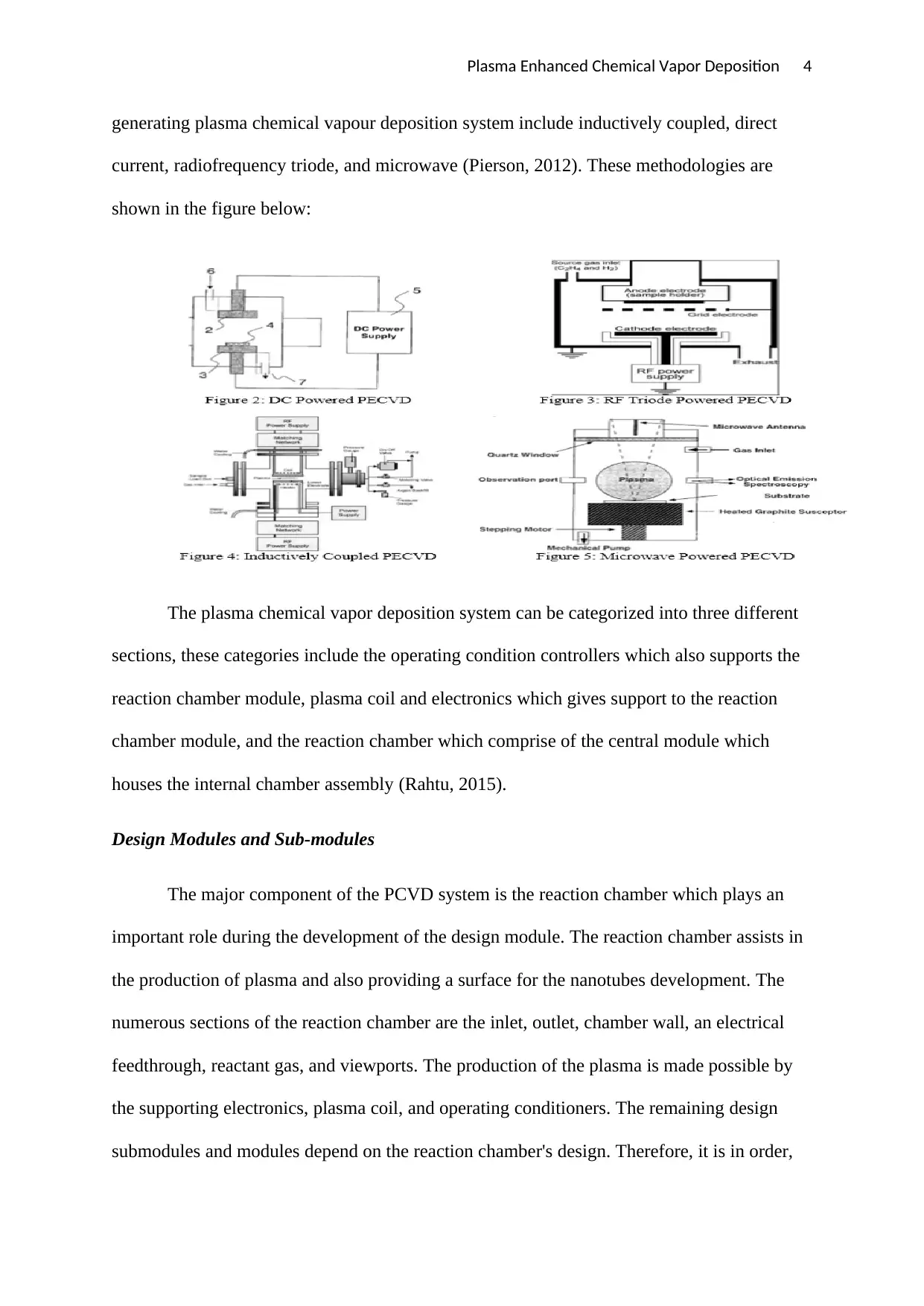
generating plasma chemical vapour deposition system include inductively coupled, direct
current, radiofrequency triode, and microwave (Pierson, 2012). These methodologies are
shown in the figure below:
The plasma chemical vapor deposition system can be categorized into three different
sections, these categories include the operating condition controllers which also supports the
reaction chamber module, plasma coil and electronics which gives support to the reaction
chamber module, and the reaction chamber which comprise of the central module which
houses the internal chamber assembly (Rahtu, 2015).
Design Modules and Sub-modules
The major component of the PCVD system is the reaction chamber which plays an
important role during the development of the design module. The reaction chamber assists in
the production of plasma and also providing a surface for the nanotubes development. The
numerous sections of the reaction chamber are the inlet, outlet, chamber wall, an electrical
feedthrough, reactant gas, and viewports. The production of the plasma is made possible by
the supporting electronics, plasma coil, and operating conditioners. The remaining design
submodules and modules depend on the reaction chamber's design. Therefore, it is in order,
Paraphrase This Document
Need a fresh take? Get an instant paraphrase of this document with our AI Paraphraser
Plasma Enhanced Chemical Vapor Deposition 5
to begin with the reaction chamber design before continuing with the design of other modules
(Richard, 2010).
The sub-modules which can be produced during the process of design include the
adjustable electrode and the internal assembly chamber. The adjustable electrode assists in
coming up with the preliminary design concept and is comprised of an automatic height
adjustment concept that uses a DC motor so as to displace the wheel and also maintaining the
difference in pressure in the chamber and outside atmosphere. In the manually adjustable
electrode, a rod that is threaded joined to the rod that is rotating is applied which in turn
moves downward and upward (Seshan, 2012).
Design of PECVD
The remote plasma source is the most appropriate method for designing of the plasma
enhanced chemical vapour deposition since this method assist greatly in disconnecting the
plasma and electric field and also enabling the system to be more adjustable. A box shape
PECVD is important since it helps in promoting and easy access to the substrate. The
complete design of the plasma enhanced chemical vapour deposition is composed of three
major sections namely quartz and the main reaction chamber. There is also internal chamber
assembly which is made up of the various components of heating and holder to the substrate.
There is also the base and the support which is made up of the base system, internal system,
chamber support, and infrared sensor (Sherman, 2014).
The figure below shows the design of the plasma enhanced chemical vapour
deposition:
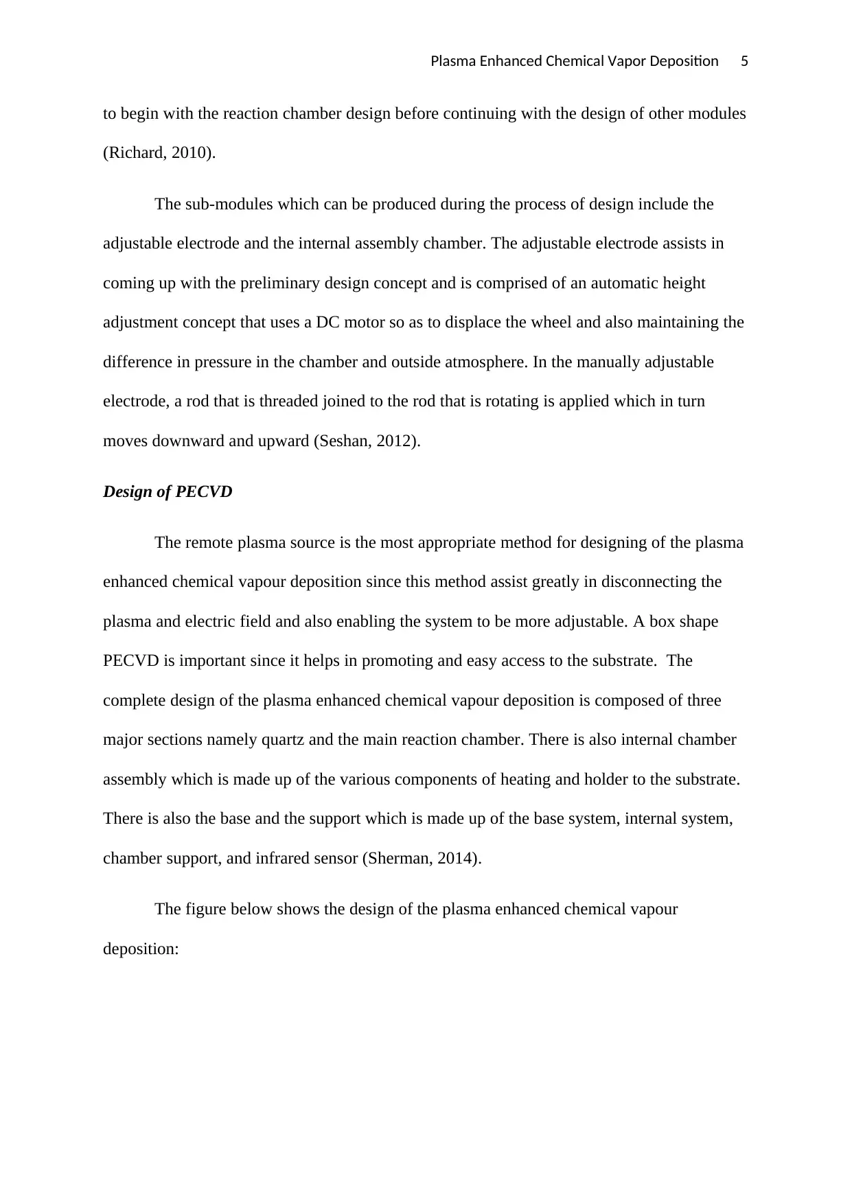
Plasma Enhanced Chemical Vapor Deposition 6
Figure 6: Three subassemblies of the PECVD (Tavares, 2013)
Chamber: The chamber is made up of 2inch diameter and with a fitting on the left section of
the chamber to allow gas entry. The tube is enclosed with copper material that is joined to the
generator of radio frequency which is involved in the generation of the plasma.
Internal Subassembly: The internal subassembly is normally deigned to provide an efficient
and safe environment for both the growing carbon nanotubes and internal components. The
quartz rods provides support to the assembly and maintain the system tray and chamber
electrically.
Support and base system: The base assist is provision of support to the entire system and is
normally made of aluminium plate. There is need to provide support to the system for it to be
in good and fixed position (Zhang, 2012).
Electronic components: There are many electrical connections throughput the entire system.
The source acts as a generator while the plasma acts as the load. Therefore, there is a
matching that is automatic which joins the generator and the load. The system is wrapped by
the use of copper mesh so as to reduce the disturbances that may be as a result of the
surrounding of the system (Pierson, 2012).
Failure Analysis
There is need of adopting possible failures in the system, the impacts of the failures to
the system, and the actions required to avoid such failures from occurring through failure
⊘ This is a preview!⊘
Do you want full access?
Subscribe today to unlock all pages.
Trusted by 1+ million students worldwide
Plasma Enhanced Chemical Vapor Deposition 7
effect and mode analysis. The categories of failures in the system can be mechanical, fluid
pressure, electrical, human factors, temperature, environment, biological and radiation.
Electrical failure may be caused by live parts, lack or grounding, arcing, improper wiring,
power supply interruption, and coil winding around quartz tube. Biological failure affects
both the skin and the eye in case of leakage of methane leading to irritation (Ostrikov, 2011).
The quartz tube temperature could surpass the O-ring’s maximum service temperature
which may lead to mechanical failure. The basic requirement when working around the CNT
is to wear gloves, failure in which may lead to electric shock while handling electrical
circuits. Hydrogen being one of the reactant gases may leak from the system leading to fire
hazard since it is highly flammable. Other reactant gases which are flammable and pose a
potential fire hazards include methane, hydrogen, and helium (Chopra, 2012).
Environmental Impacts
The manufacturing of quartz and stainless steel impacts negatively on the climatic
change, ozone layer, eco-toxicity, acidity, land use, and minerals. Majority of the
environmental impacts are as a result of the stainless steel. These environmental impacts can
be minimized by the use of different material which may pose a challenge because the
stainless steel is readily available to be utilized in the chamber of the system. The stainless
steel is also appropriate in non-reactive conditions and less expensive making it capable
enduring plasma. The manufacture of quartz and stainless steel also has some effects on the
health of humans (Richard, 2010).
Paraphrase This Document
Need a fresh take? Get an instant paraphrase of this document with our AI Paraphraser
Plasma Enhanced Chemical Vapor Deposition 8
Bibliography
Chopra, K., 2012. Thin Film Device Applications. illustrated ed. Nawanshahr: Springer Science &
Business Media.
Franssila, S., 2010. Introduction to Microfabrication. 2 ed. Helsinki: John Wiley & Sons.
Konuma, B., 2011. Film Deposition by Plasma Techniques. Prentice Hall: Spring-Verlag.
Mattox, D. M., 2016. Handbook of Physical Vapor Deposition (PVD) Processing. revised ed. Kentucky:
William Andrew.
Ostrikov, K., 2011. PLASMA NANOSCIENCE. SYDNEY: JOHN WILEY AND SONS.
Pierson, H. O., 2012. Handbook of Chemical Vapor Deposition: Principles, Technology and
Applications. Paris: Elsevier Science.
Rahtu, A., 2015. Atomic Layer Deposition of High Permittivity Oxides: Film Growth and In Situ Studies.
Perth: University of Helsinki.
Richard, C., 2010. Introduction to Microelectronic Fabrication. New York: Upper Saddle River.
Seshan, K., 2012. Handbook of Thin Film Deposition: Techniques, Processes, and Technologies.
illustrated, revised ed. Arizona: William Andrew.
Sherman, K., 2014. hemical Vapor Deposition for Microelectronics Principles, Technology, and
Applications. Harrow: Noyes Publications.
Tavares, L., 2013. Plasma Synthesis of Coated Metal Nanoparticles with Surface Properties Tailored
for Dispersion. Colorado: Plasma Processes and Polymers.
Zhang, Q., 2012. Advances in Nanodevices and Nanofabrication: Selected Publications from
Symposium of Nanodevices and Nanofabrication in ICMAT. illustrated ed. london: CRC Press.
1 out of 8

Your All-in-One AI-Powered Toolkit for Academic Success.
+13062052269
info@desklib.com
Available 24*7 on WhatsApp / Email
![[object Object]](/_next/static/media/star-bottom.7253800d.svg)
Unlock your academic potential
Copyright © 2020–2026 A2Z Services. All Rights Reserved. Developed and managed by ZUCOL.