Design of Common Source Amplifier: Competency Demonstration Report
VerifiedAdded on 2022/08/28
|9
|1613
|15
Report
AI Summary
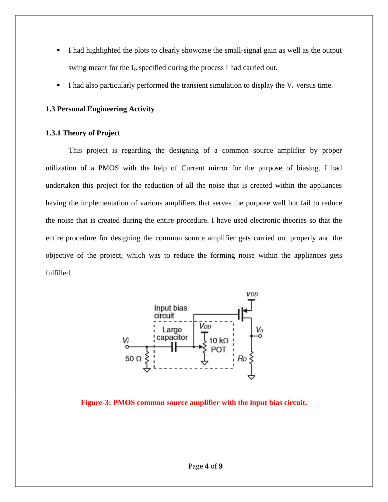
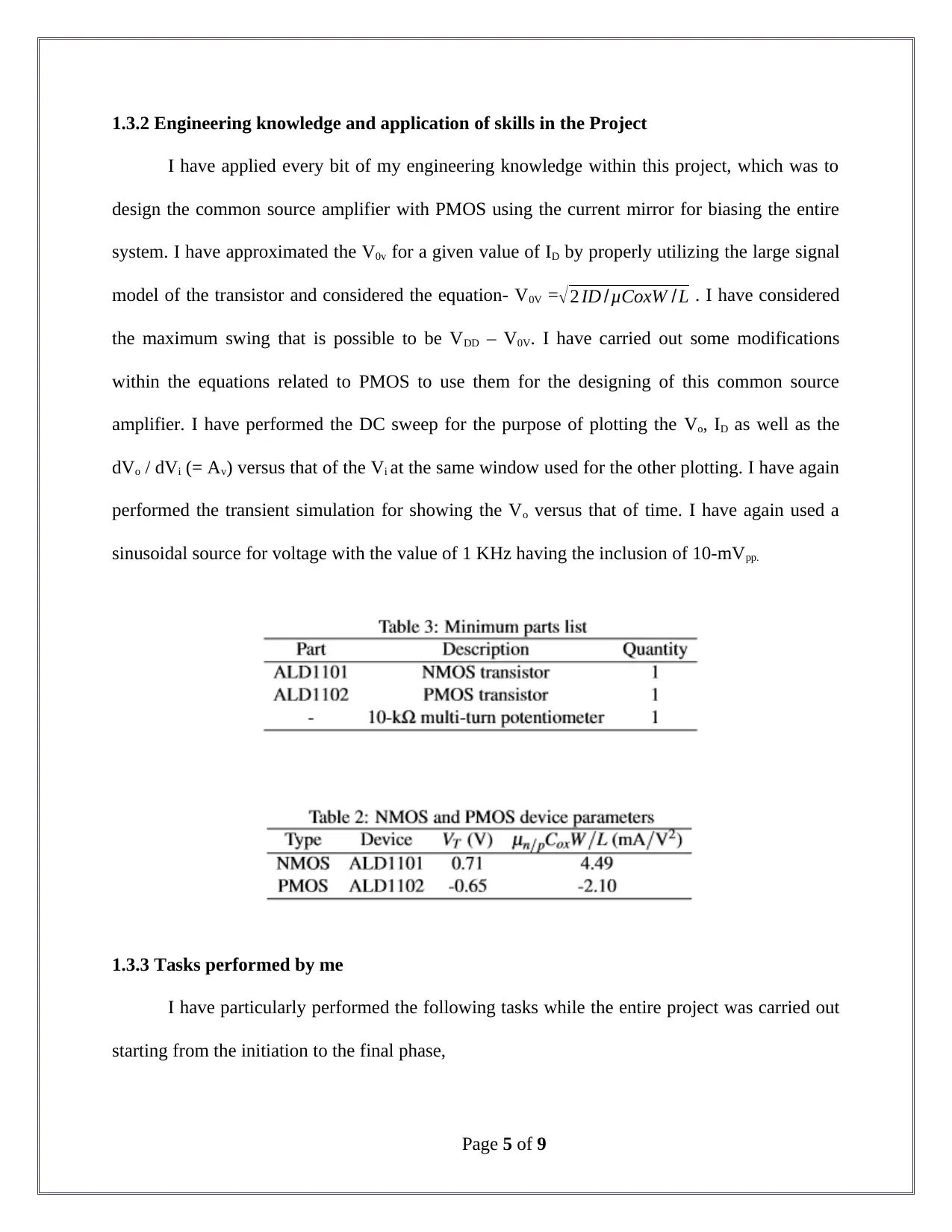
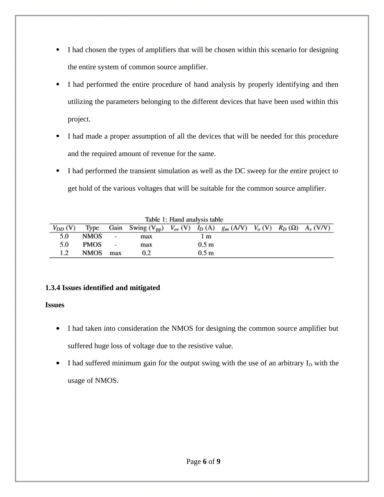
This report details the design of a single-stage common source amplifier with a PMOS load, utilizing a current mirror for biasing. The project, undertaken at Macquarie University as part of a Master of Engineering program, focuses on reducing noise in electronic appliances. The student's responsibiliti...

Competency Demonstration Report (CDR)
Career Episode 1
Career Episode 1
Secure Best Marks with AI Grader
Need help grading? Try our AI Grader for instant feedback on your assignments.

1.0 Career Episode- 1
1.1 Introduction
Project Name: - Design of a Single Stage Common Source Amplifier with PMOS Load
Using Current Mirror for the Biasing.
Location of the Project: - Macquarie University, Sydney, Australia.
Duration of the project: - [Please fill].
Organization: - Macquarie University.
Position within Project: - Masters of Engineering (Electronics Engineering Major)
postgraduate student.
1.2 Background
1.2.1 Characteristics of the Project
This project deals with the designing of a Single Stage Common Source Amplifier with
the help of a PMOS load utilizing the Current Mirror for the Biasing. The proposed system has
the primary inclusion of a CMOS analog circuits along with a resistive load for a better
designing of the entire amplifier to provision the common usage of this amplifier into various
applications for sensor signal amplification as well as RF-low noise amplification within the
circuits as well as the appliances. Within this undertaken project, PMOS has been used for better
results of the expected outcome.
Page 1 of 9

1.2.2 Objective of the Project
Primarily the objective for which this project had been undertaken is to reduce
the noise produced within the appliances that make use of multiply existing types of amplifiers
as a result of which, noise increases along with the usage of such appliances. To obtain this
particular objective, PMOS has been implemented within the source amplifiers having the
inclusion of a resistive load to be designed for different kinds of requirements such as the like of
gain, supply voltage as well as swing. I had worked within the team as a postgraduate student for
Masters of Engineering to build the entire system by using all the technologies and the gadgets
that have been properly installed within the system to get hold of the expected outcomes.
1.2.3 My work area
I was assigned to work upon this project along with my team members to build up and
design this common source amplifier with the help of PMOS load utilizing current mirror for the
purpose of biasing the same. I had performed the hand analysis properly utilizing the parameters
belonging to the device that have been used for designing of the system. I had performed the
point simulation that is properly DC operated for all the amplifiers that have been considered in
the above. In addition to this, I have also performed the activities that include the performing of
DC sweep, transient simulation and lastly, organizing the results of the procedure as a part of
presenting the same using TA.
Figure-1: The above diagram highlights the PMOS common source amplifier.
Page 2 of 9

1.2.4 Organization chart
Figure-2: Chronology of the Organization
1.2.5 My responsibilities
I had carried out the following activities throughout the entire process of designing the
common source amplifier using PMOS load,
I had designed the entire system of the amplifier with the usage of PMOS load as a part
of current mirror for the purpose of biasing.
I had particularly performed the process of hand analysis with the help of all the
parameters belonging to the designs for designing the common source amplifier.
I had performed the simulation for the DC operating point in regards to all of the
amplifiers needed to be taken into account for this entire process.
I had performed the DC sweep in order to plot the Vo, ID as well as the dVo / dVi (= Av)
versus that of the Vi.
Page 3 of 9
Secure Best Marks with AI Grader
Need help grading? Try our AI Grader for instant feedback on your assignments.

I had highlighted the plots to clearly showcase the small-signal gain as well as the output
swing meant for the ID specified during the process I had carried out.
I had also particularly performed the transient simulation to display the Vo versus time.
1.3 Personal Engineering Activity
1.3.1 Theory of Project
This project is regarding the designing of a common source amplifier by proper
utilization of a PMOS with the help of Current mirror for the purpose of biasing. I had
undertaken this project for the reduction of all the noise that is created within the appliances
having the implementation of various amplifiers that serves the purpose well but fail to reduce
the noise that is created during the entire procedure. I have used electronic theories so that the
entire procedure for designing the common source amplifier gets carried out properly and the
objective of the project, which was to reduce the forming noise within the appliances gets
fulfilled.
Figure-3: PMOS common source amplifier with the input bias circuit.
Page 4 of 9

1.3.2 Engineering knowledge and application of skills in the Project
I have applied every bit of my engineering knowledge within this project, which was to
design the common source amplifier with PMOS using the current mirror for biasing the entire
system. I have approximated the V0v for a given value of ID by properly utilizing the large signal
model of the transistor and considered the equation- V0V =√ 2 ID /μCoxW /L . I have considered
the maximum swing that is possible to be VDD – V0V. I have carried out some modifications
within the equations related to PMOS to use them for the designing of this common source
amplifier. I have performed the DC sweep for the purpose of plotting the Vo, ID as well as the
dVo / dVi (= Av) versus that of the Vi at the same window used for the other plotting. I have again
performed the transient simulation for showing the Vo versus that of time. I have again used a
sinusoidal source for voltage with the value of 1 KHz having the inclusion of 10-mVpp.
1.3.3 Tasks performed by me
I have particularly performed the following tasks while the entire project was carried out
starting from the initiation to the final phase,
Page 5 of 9

I had chosen the types of amplifiers that will be chosen within this scenario for designing
the entire system of common source amplifier.
I had performed the entire procedure of hand analysis by properly identifying and then
utilizing the parameters belonging to the different devices that have been used within this
project.
I had made a proper assumption of all the devices that will be needed for this procedure
and the required amount of revenue for the same.
I had performed the transient simulation as well as the DC sweep for the entire project to
get hold of the various voltages that will be suitable for the common source amplifier.
1.3.4 Issues identified and mitigated
Issues
I had taken into consideration the NMOS for designing the common source amplifier but
suffered huge loss of voltage due to the resistive value.
I had suffered minimum gain for the output swing with the use of an arbitrary ID with the
usage of NMOS.
Page 6 of 9
Paraphrase This Document
Need a fresh take? Get an instant paraphrase of this document with our AI Paraphraser

Mitigation
To mitigate the problem that I had specifically faced with the usage of NMOS for
building the entire system, I had taken the decision of using the PMOS for designing the
common source amplifier.
I had taken the decision of gaining the maximum output by removing the NMOS from
the designing procedure and replacing it with the PMOS to design the common source
amplifier.
1.3.5 Collaborated work
I had specifically placed forward the proposal of designing such a common source
amplifier with the help of PMOS to reduce the noise that is produced within the appliances that
are commonly built. In the procedure for this project, I have worked successfully with all of the
members who belonged to my team to design the entire amplifier with all the required devices
and appliances that is needed successfully under the team leader.
1.4 Summary
1.4.1 Overview of the Project
The entire project was to design a common source amplifier by implementing the PMOS
using the current mirror for the purpose of biasing. I have utilized the entire knowledge that I
gathered during the entire time period of my post-graduation and graduation for a successful
implementation of the same within the project and to acquire the expected results for an efficient
amplifier with reduced amount of noise.
Page 7 of 9

1.4.2 Meeting of the goals
Initially, the prime goal as well as the objective of the project was to reduce the noise that
is produced from the appliances that includes the installation of many types of amplifiers, and to
replace them by designing and building a common source single stage amplifier using PMOS
with the help of current mirror for attaining the objective of biasing. By properly using and
implementing all the required devices and appliances, the project was successfully completed by
meeting all the initial objectives of the project.
1.4.3 Personal Contribution
I had particularly worked towards the choosing of all the required devices as well as the
appliances including the decision whether to choose NMOS or PMOS for the designing of the
single stage amplifier. I had carried out a number of activities such as the like of performing the
hand analysis, transient simulation for the system along with the DC sweep that was necessary
for designing the entire system in the proper way to get hold of the expected results in the end. I
had also presented the entire results of all the procedures that have been carried out within the
table using TA along with the other forms of data.
Page 8 of 9
1 out of 9
Related Documents

Your All-in-One AI-Powered Toolkit for Academic Success.
+13062052269
info@desklib.com
Available 24*7 on WhatsApp / Email
Unlock your academic potential
© 2024 | Zucol Services PVT LTD | All rights reserved.