Communications Technology 2 Assignment Solution - DCU 2019-2020
VerifiedAdded on 2022/08/14
|12
|1044
|14
Homework Assignment
AI Summary
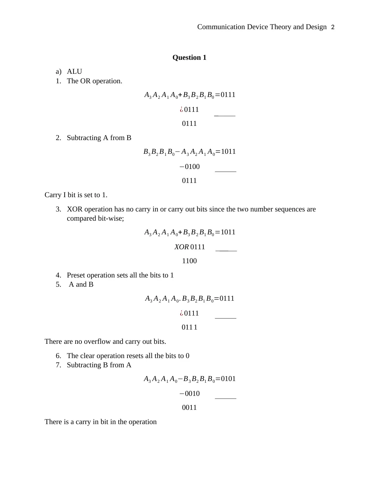
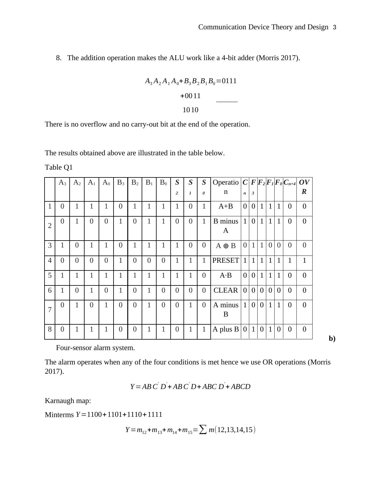
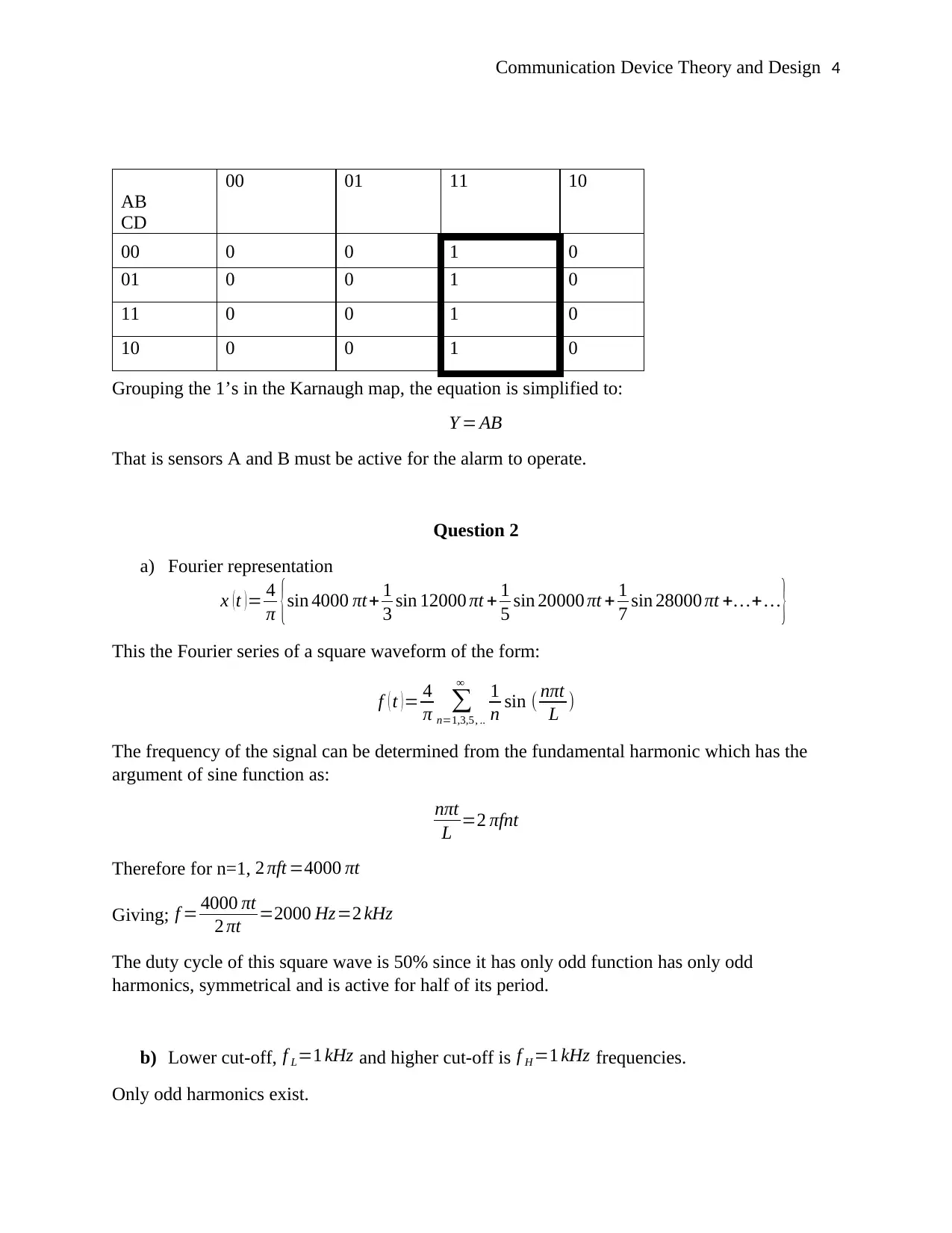
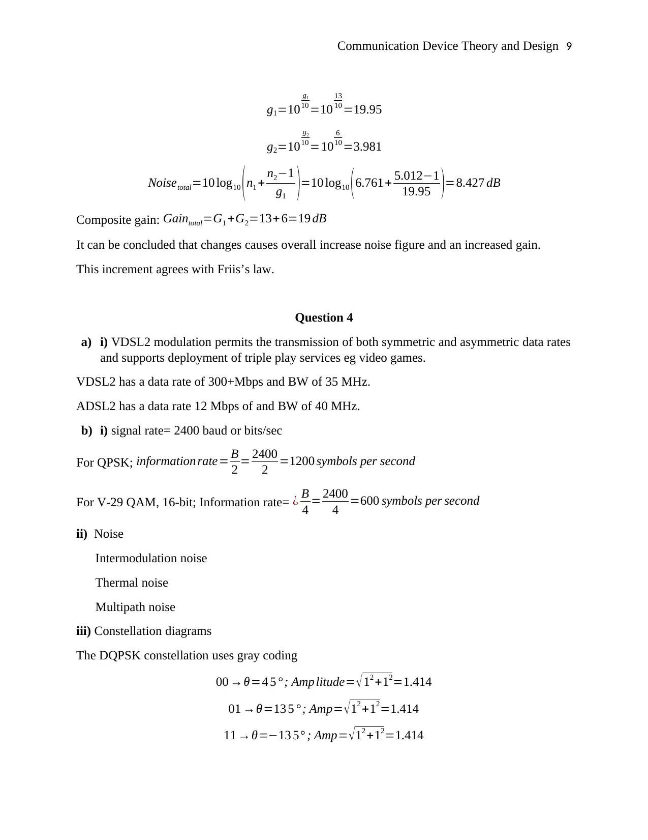
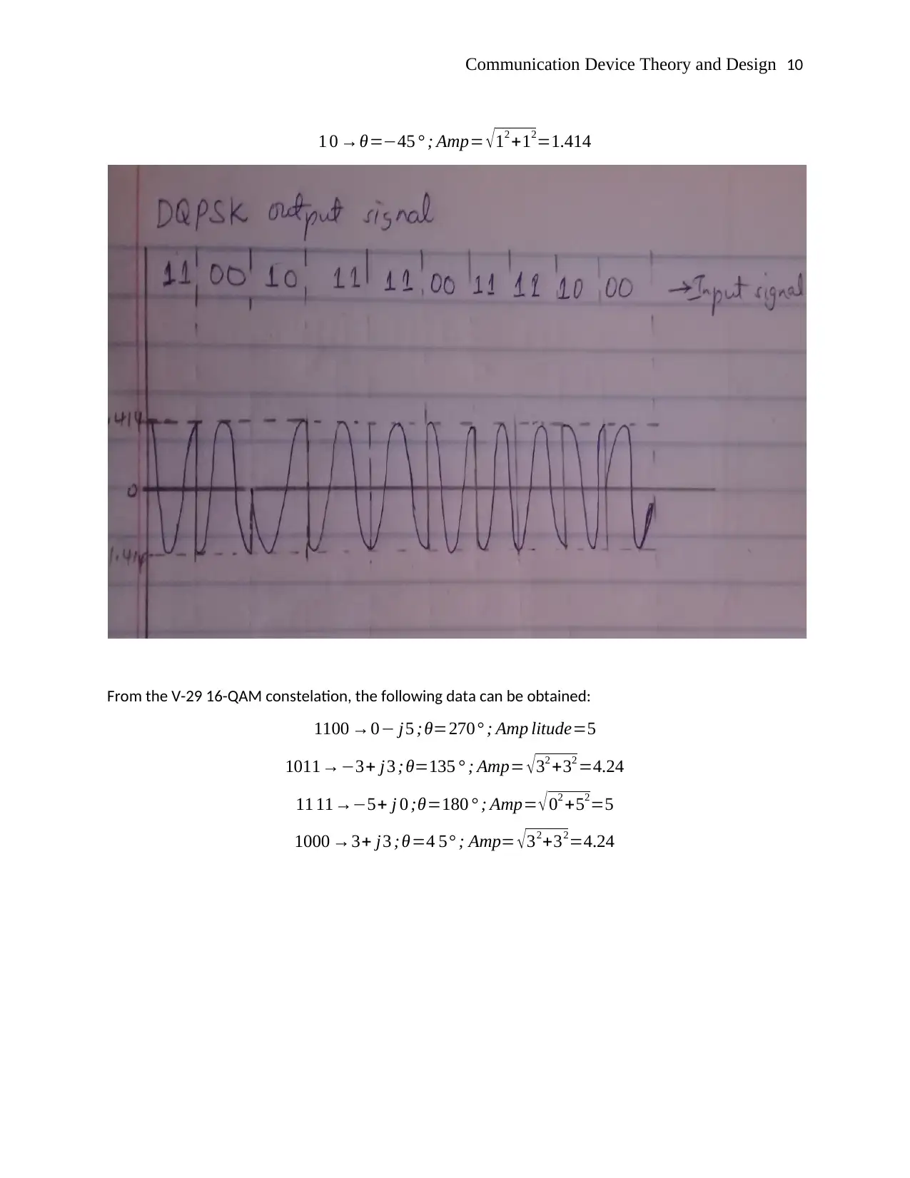
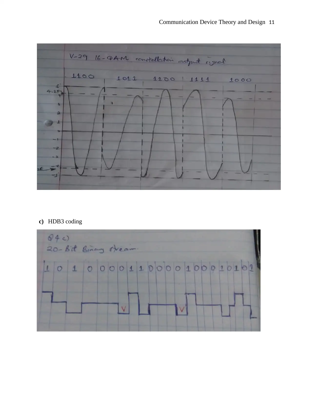
This document presents a comprehensive solution to a Communications Technology assignment, covering multiple key areas within the field. The first section focuses on the Arithmetic Logic Unit (ALU), detailing various operations like OR, XOR, preset, clear, addition, and subtraction, with corresponding truth tables and explanations. The second part delves into Fourier representation, analyzing a square waveform, calculating harmonic frequencies, and demonstrating the effects of band-pass and low-pass filters. The third section explores RLC circuits, including resonant frequency, Q-factor, and bandwidth, along with their applications in signal processing and communication systems, followed by a discussion on composite noise figures and gain. Finally, the assignment addresses VDSL2 modulation, comparing it to ADSL2, and covering topics such as signal rate, noise, and constellation diagrams, including HDB3 coding.

Communication Device Theory and Design 1
COMMUNICATION DEVICE THEORY AND DESIGN
by (Name)
Course Name
Professor (Tutor) Name
Name of University/School
City and State
Date
COMMUNICATION DEVICE THEORY AND DESIGN
by (Name)
Course Name
Professor (Tutor) Name
Name of University/School
City and State
Date
Paraphrase This Document
Need a fresh take? Get an instant paraphrase of this document with our AI Paraphraser

Communication Device Theory and Design 2
Question 1
a) ALU
1. The OR operation.
A3 A2 A1 A0+ B3 B2 B1 B0 =0111
¿ 0111
0111
2. Subtracting A from B
B3 B2 B1 B0− A3 A2 A1 A0=1011
−0100
0111
Carry I bit is set to 1.
3. XOR operation has no carry in or carry out bits since the two number sequences are
compared bit-wise;
A3 A2 A1 A0+ B3 B2 B1 B0 =1011
XOR 0111
1100
4. Preset operation sets all the bits to 1
5. A and B
A3 A2 A1 A0 . B3 B2 B1 B0=0111
¿ 0111
011 1
There are no overflow and carry out bits.
6. The clear operation resets all the bits to 0
7. Subtracting B from A
A3 A2 A1 A0−B3 B2 B1 B0=0101
−0010
0011
There is a carry in bit in the operation

Communication Device Theory and Design 3
8. The addition operation makes the ALU work like a 4-bit adder (Morris 2017).
A3 A2 A1 A0+ B3 B2 B1 B0 =0111
+00 11
10 10
There is no overflow and no carry-out bit at the end of the operation.
The results obtained above are illustrated in the table below.
Table Q1
b)
Four-sensor alarm system.
The alarm operates when any of the four conditions is met hence we use OR operations (Morris
2017).
Y = AB C' D'+ AB C' D+ ABC D' + ABCD
Karnaugh map:
Minterms Y =1100+1101+1110+1111
Y =m12 +m13+ m14 +m15=∑ m(12,13,14,15)
A3 A2 A1 A0 B3 B2 B1 B0 S
2
S
1
S
0
Operatio
n
C
n
F
3
F2 F1 F0 Cn+4 OV
R
1 0 1 1 1 0 1 1 1 1 0 1 A+B 0 0 1 1 1 0 0
2 0 1 0 0 1 0 1 1 0 0 1 B minus
A
1 0 1 1 1 0 0
3 1 0 1 1 0 1 1 1 1 0 0 A ⊕ B 0 1 1 0 0 0 0
4 0 0 0 0 1 0 0 0 1 1 1 PRESET 1 1 1 1 1 1 1
5 1 1 1 1 1 1 1 1 1 1 0 A∙B 0 0 1 1 1 0 0
6 1 0 1 0 1 0 1 0 0 0 0 CLEAR 0 0 0 0 0 0 0
7 0 1 0 1 0 0 1 0 0 1 0 A minus
B
1 0 0 1 1 0 0
8 0 1 1 1 0 0 1 1 0 1 1 A plus B 0 1 0 1 0 0 0
⊘ This is a preview!⊘
Do you want full access?
Subscribe today to unlock all pages.

Trusted by 1+ million students worldwide

Communication Device Theory and Design 4
AB
CD
00 01 11 10
00 0 0 1 0
01 0 0 1 0
11 0 0 1 0
10 0 0 1 0
Grouping the 1’s in the Karnaugh map, the equation is simplified to:
Y = AB
That is sensors A and B must be active for the alarm to operate.
Question 2
a) Fourier representation
x ( t ) = 4
π {sin 4000 πt+ 1
3 sin 12000 πt + 1
5 sin 20000 πt + 1
7 sin 28000 πt +…+ … }
This the Fourier series of a square waveform of the form:
f ( t )= 4
π ∑
n=1,3,5, ..
∞ 1
n sin ( nπt
L )
The frequency of the signal can be determined from the fundamental harmonic which has the
argument of sine function as:
nπt
L =2 πfnt
Therefore for n=1, 2 πft =4000 πt
Giving; f = 4000 πt
2 πt =2000 Hz=2 kHz
The duty cycle of this square wave is 50% since it has only odd function has only odd
harmonics, symmetrical and is active for half of its period.
b) Lower cut-off, f L=1 kHz and higher cut-off is f H =1 kHz frequencies.
Only odd harmonics exist.
Paraphrase This Document
Need a fresh take? Get an instant paraphrase of this document with our AI Paraphraser

Communication Device Theory and Design 5
Using fundamental harmonic frequency; 2 πf =4000 π, f 0=2 kHz
Third harmonic frequency; f 1=12000 π
2 π =6 kHz
Fifth harmonic frequency; f 2= 20000 π
2 π =10 kHz
Seventh harmonic frequency; f 3= 28000 π
2 π =14 kHz
Therefore, the seventh and higher order harmonics are filtered out by the ideal band-pass filter
(Stranneby and Walker 2014).
The filter output is:
x (t )= 4
π {sin 4000 πt+ 1
3 sin 12000 πt + 1
5 sin 20000 πt }
Passing the filter output through an ideal amplifier with a gain of -10 gives the following
output.
x ( t ) =−40
π {sin 4000 πt+ 1
3 sin 12000 πt + 1
5 sin 20000 πt }
Using Excel to graph the output of the amplifier, we get:
0 5 10 15 20 25 30
-40
-30
-20
-10
0
10
20
30
40
Amplifier output for BPF
c) Value of capacitor:

Communication Device Theory and Design 6
f = 1
2 πRC = 1
2 π × 2000× C =16000
C= 1
2 π ×2000 ×16000 =4.974 nF
Output of filter:
X c=R=2 k Ω
v0 ( t )= Xc
Xc+ R vi ( t )
v0 ( t )= 2
2+2 vi ( t )=0.5 vi ( t )
With LPF of 16 kHz cut-off frequency, the input signal becomes:
v0 ( t )=0.5 ×−10 × 4
π {sin 4000 πt + 1
3 sin 12000 πt + 1
5 sin 20000 πt }
v0 ( t )=−20
π {sin 4000 πt+ 1
3 sin12000 πt+ 1
5 sin 20000 πt }
0 5 10 15 20 25 30 35 40 45
-20
-15
-10
-5
0
5
10
15
20 Amplifier Output for LPF
d) The signals at the outputs of the Band-Pass filter of part b) and Low-Pass filter of part c)
are similar since they possess the same number of harmonics of the given input signal.
⊘ This is a preview!⊘
Do you want full access?
Subscribe today to unlock all pages.

Trusted by 1+ million students worldwide

Communication Device Theory and Design 7
However, the signal at the output of the LPF is attenuated and has amplitude half that of
the BPF output signal. The signals have the same phase response of the harmonic
components (Stranneby and Walker 2014).
Question 3
a) Q3 a).
In figure 3 a), a series RLC circuit is illustrated
C=1.6 pF , L=1.6 μF∧R=10 Ω
i) Resonant frequency of the circuit.
At resonance, X L=Xc
1
2 πfC =2 πfL
∴ f r= 1
2 π √ LC = 1
2 π √ 1.6 × 10−12 × 1.6 ×10−6 =99.472 MHz
ii) Q-factor at resonance
Q= X L
R = Xc
R = 2 π ×99.472 ×106 ×1.6 × 10−6
10 =100
The bandwidth of the circuit
BW = f r
Q = 99.472×10⁶
100 =994.72 kHz
iii) Reducing R to 2.5 Ω
New Q-factor and Bandwidth
Q= X L
R = 2 π × 99.472×106 × 1.6 ×10−6
2.5 =400
BW = f r
Q = 99.472×10⁶
400 =248.680 kHz
Since the bandwidth has reduced, the circuit is more selective with R=2.5 Ω than with R=10 Ω
iv) In figure 3 b), reduced value of resistances is seen compared to the configuration of
figure 3 a) since the internal resistances of the capacitor and inductor cancels out.
Paraphrase This Document
Need a fresh take? Get an instant paraphrase of this document with our AI Paraphraser

Communication Device Theory and Design 8
Reducing the value of resistance leads to increased Q-factor and reduced bandwidth. This
increases the selectivity of the parallel LC circuit (Stranneby and Walker 2014).
Series RLC circuits are mainly used in signal processing and communication systems in
applications such tuning radio TXs and RXs.
Parallel LC circuits are used in induction heating circuits and also for voltage magnification
b) Composite noise figure
N1=8 dB ,G1=10 dB; N2 =7 dB , G2=6 dB
Noisetotal=10 log10
( ni +∑
i=2
M ni−1
∏
j=1
i−1
gi )
n1=10
N 1
10 =10
8
10 =6.31
n2 =10
N 2
10 =10
7
10 =5.012
g1=10
g1
10 =10
10
10 =10
g2=10
g2
10 =10
6
10 =3.981
Noisetotal=10 log10 (n1 + n2−1
g1 )=10 log10 (6.31+ 5.012−1
10 )=8.268 dB
Composite gain: Gaintotal=G1 +G2=10+6=16 dB
Increasing gain and noise figures of the input amplifier:
New values
N1=8+ 0.3=8.3 dB
G1=10+3=13 dB
Calculating new composite noise figure:
n1=10
N 1
10 =10
8.3
10 =6.761
n2 =10
N 2
10 =10
7
10 =5.012

Communication Device Theory and Design 9
g1=10
g1
10 =10
13
10 =19.95
g2=10
g2
10 =10
6
10 =3.981
Noisetotal=10 log10 (n1 + n2−1
g1 )=10 log10 (6.761+ 5.012−1
19.95 )=8.427 dB
Composite gain: Gaintotal=G1 +G2=13+6=19 dB
It can be concluded that changes causes overall increase noise figure and an increased gain.
This increment agrees with Friis’s law.
Question 4
a) i) VDSL2 modulation permits the transmission of both symmetric and asymmetric data rates
and supports deployment of triple play services eg video games.
VDSL2 has a data rate of 300+Mbps and BW of 35 MHz.
ADSL2 has a data rate 12 Mbps of and BW of 40 MHz.
b) i) signal rate= 2400 baud or bits/sec
For QPSK; information rate= B
2 = 2400
2 =1200 symbols per second
For V-29 QAM, 16-bit; Information rate= ¿ B
4 = 2400
4 =600 symbols per second
ii) Noise
Intermodulation noise
Thermal noise
Multipath noise
iii) Constellation diagrams
The DQPSK constellation uses gray coding
00 →θ=4 5 ° ; Amp litude= √12 +12=1.414
01 →θ=13 5 °; Amp= √12 +12=1.414
11 →θ=−13 5° ; Amp= √12 +12=1.414
⊘ This is a preview!⊘
Do you want full access?
Subscribe today to unlock all pages.

Trusted by 1+ million students worldwide

Communication Device Theory and Design 10
1 0 →θ=−45 ° ; Amp= √12 +12=1.414
From the V-29 16-QAM constelation, the following data can be obtained:
1100 →0− j5 ; θ=270° ; Amp litude=5
1011→−3+ j 3 ; θ=135 ° ; Amp= √ 32 +32 =4.24
11 11→−5+ j 0 ;θ=180 ° ; Amp= √ 02 +52=5
1000 →3+ j3 ;θ=4 5° ; Amp= √ 32+32=4.24
1 0 →θ=−45 ° ; Amp= √12 +12=1.414
From the V-29 16-QAM constelation, the following data can be obtained:
1100 →0− j5 ; θ=270° ; Amp litude=5
1011→−3+ j 3 ; θ=135 ° ; Amp= √ 32 +32 =4.24
11 11→−5+ j 0 ;θ=180 ° ; Amp= √ 02 +52=5
1000 →3+ j3 ;θ=4 5° ; Amp= √ 32+32=4.24
Paraphrase This Document
Need a fresh take? Get an instant paraphrase of this document with our AI Paraphraser

Communication Device Theory and Design 11
c) HDB3 coding
c) HDB3 coding

Communication Device Theory and Design 12
Reference List
Morris, J. (2017). Digital Electronics. 4th ed. Texas: ROUTLEDGE, pp.132-160.
Stranneby, D. and Walker, W. (2014). Digital signal processing and applications. Amsterdam:
Elsevier/Newnes.
Reference List
Morris, J. (2017). Digital Electronics. 4th ed. Texas: ROUTLEDGE, pp.132-160.
Stranneby, D. and Walker, W. (2014). Digital signal processing and applications. Amsterdam:
Elsevier/Newnes.
⊘ This is a preview!⊘
Do you want full access?
Subscribe today to unlock all pages.

Trusted by 1+ million students worldwide
1 out of 12
Your All-in-One AI-Powered Toolkit for Academic Success.
+13062052269
info@desklib.com
Available 24*7 on WhatsApp / Email
Unlock your academic potential
Copyright © 2020–2025 A2Z Services. All Rights Reserved. Developed and managed by ZUCOL.