COMP 300 Spring 2021 Midterm Exam: Data Path Design and RTL Programs

Verified

Added on  2021/07/07

|17
|2233
|257
Homework Assignment
AI Summary
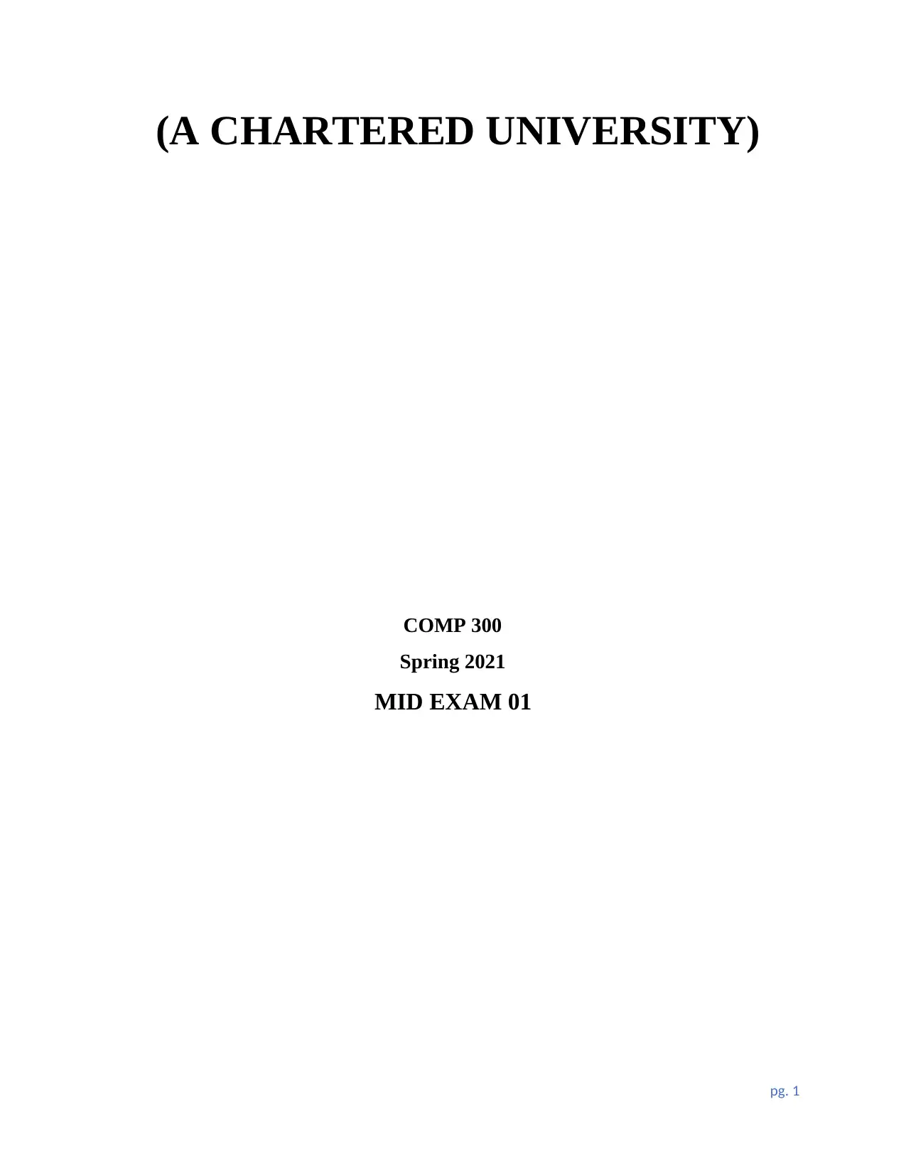
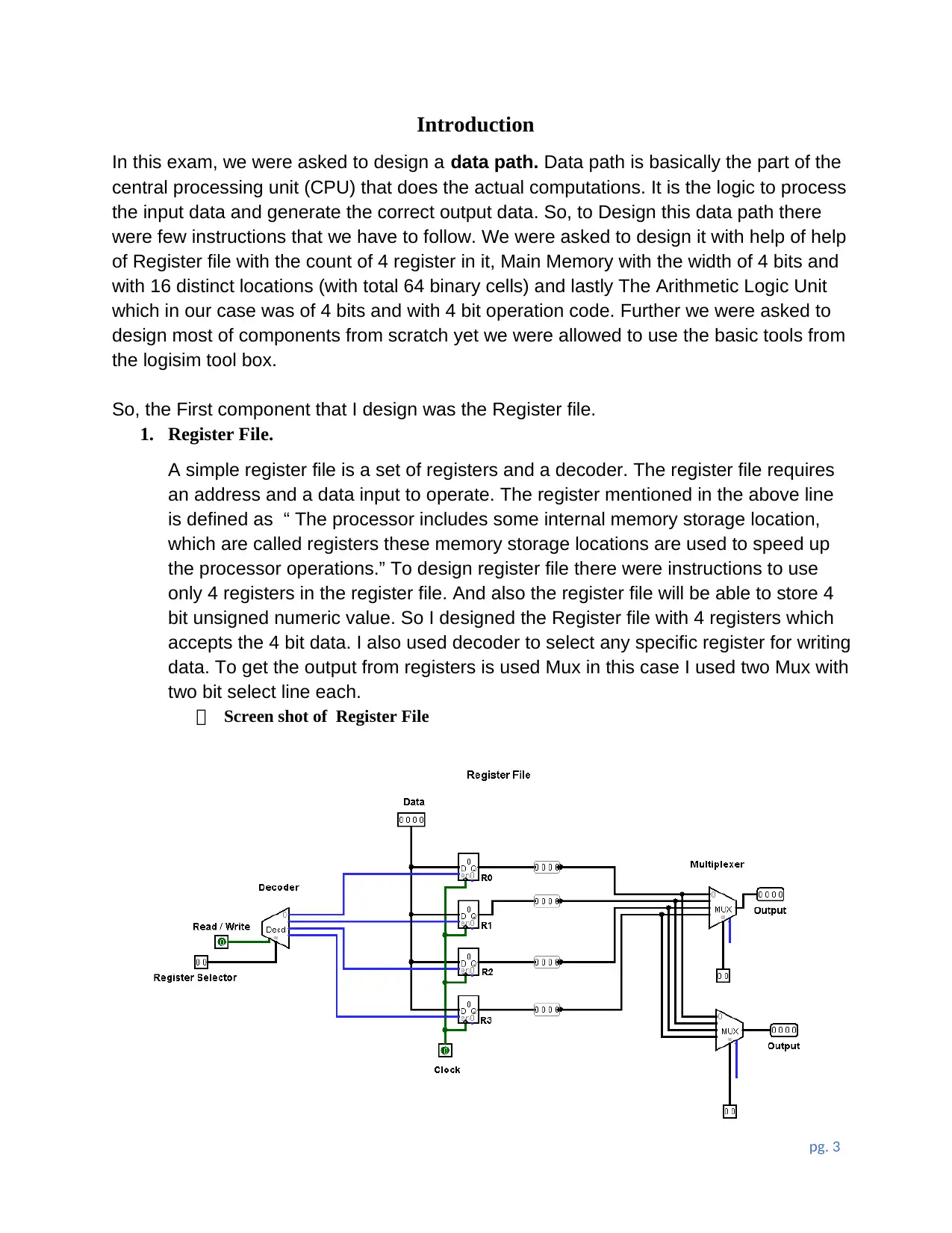
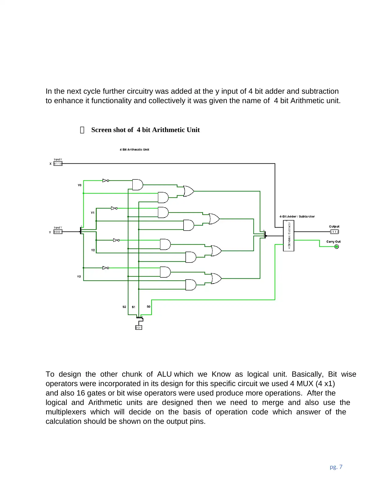
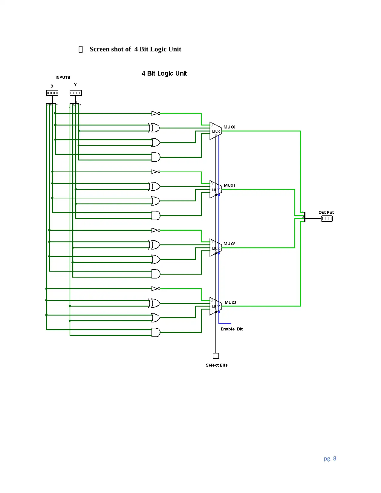
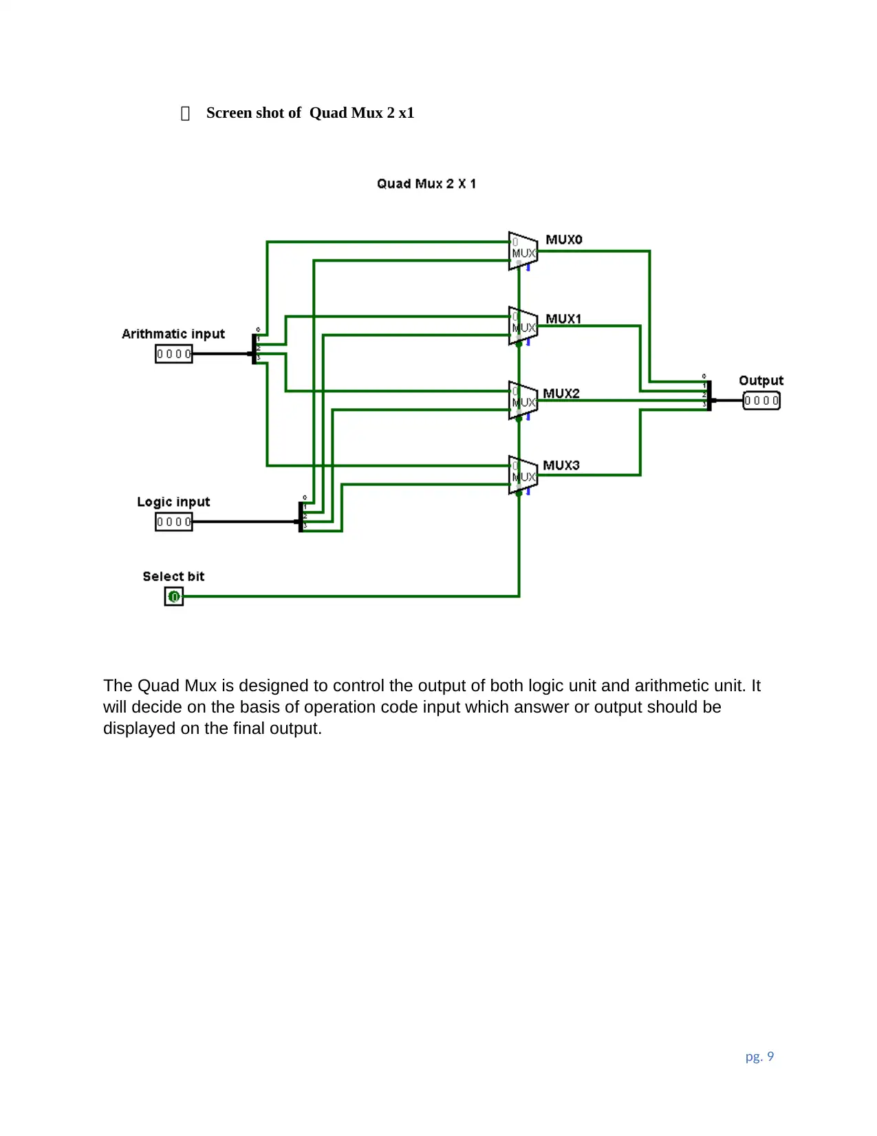
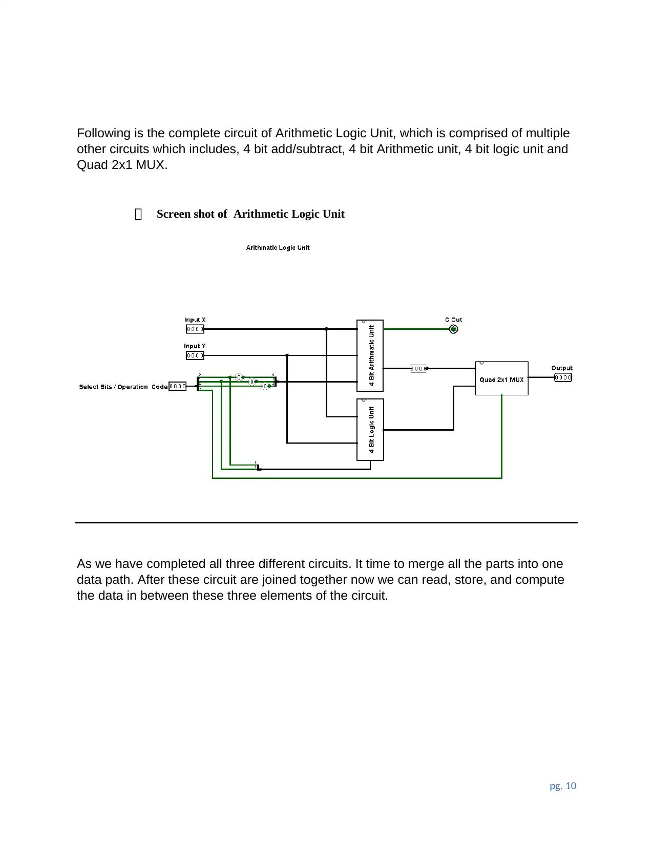
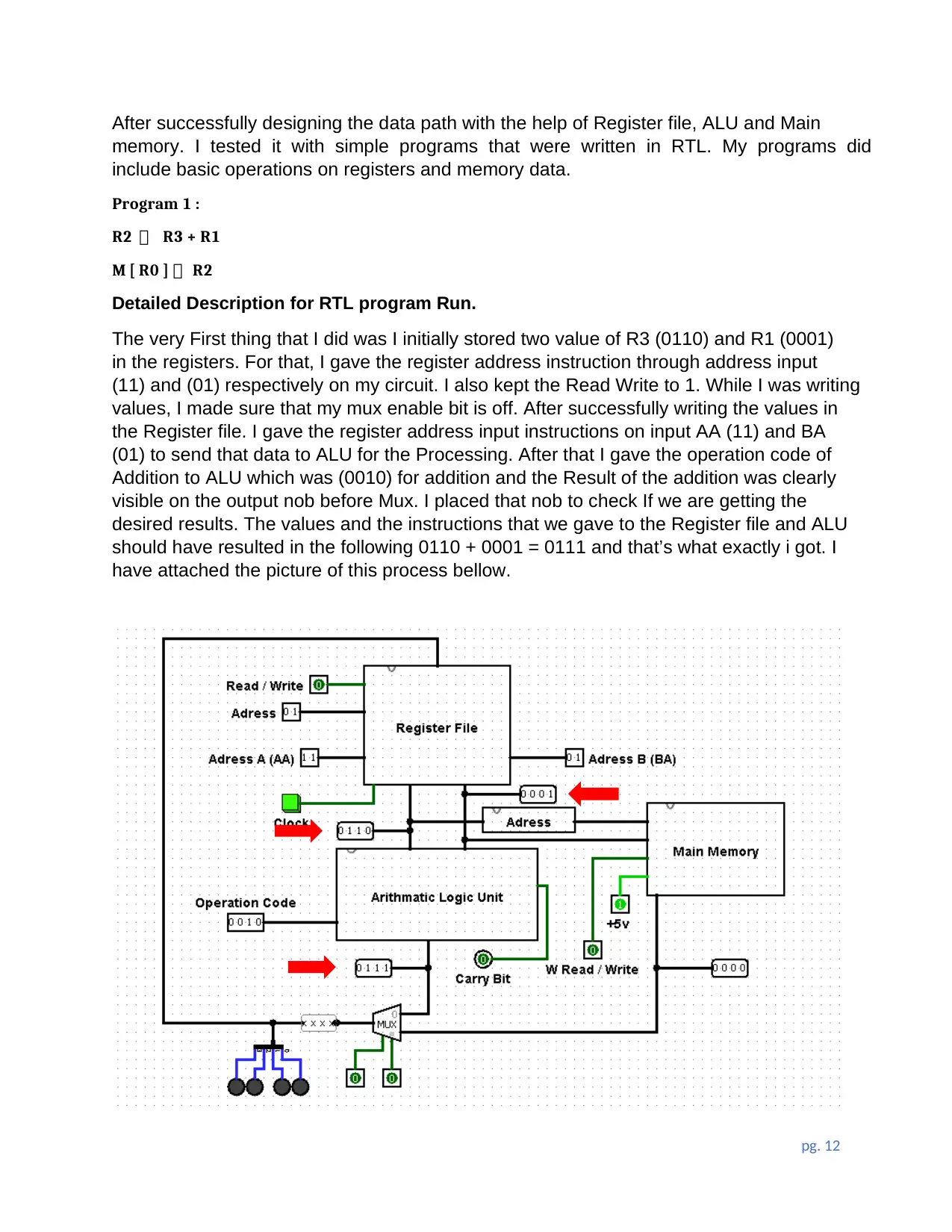
This document presents a solution to a midterm exam assignment from a Chartered University's COMP 300 course, focusing on data path design. The assignment required designing a data path consisting of a register file (4 registers), a 4-bit main memory (16 locations), and a 4-bit ALU with a 4-bit operation code. The solution details the design of each component from scratch, including the register file using decoders and multiplexers, the main memory using binary cells and decoders, and the ALU comprising arithmetic and logic units. The arithmetic unit includes a 4-bit adder/subtracter and a 4-bit arithmetic unit, while the logic unit incorporates bitwise operators. The solution merges these units and utilizes multiplexers to control the output based on the operation code. The student then tested the designed data path with two RTL programs, demonstrating operations on registers and memory data, and explaining the control signals used during the program runs. The document includes screenshots of each component and the RTL program runs, illustrating the step-by-step process of data storage, retrieval, and computation within the data path. The document also includes the components used such as decoders, registers, multiplexers, adders, and logic gates.
Document Page
pg. 1
(A CHARTERED UNIVERSITY)
COMP 300
Spring 2021
MID EXAM 01
tabler-icon-diamond-filled.svg

Paraphrase This Document

Need a fresh take? Get an instant paraphrase of this document with our AI Paraphraser
Document Page
pg. 2
Document Page
pg. 3
Introduction
In this exam, we were asked to design a data path. Data path is basically the part of the
central processing unit (CPU) that does the actual computations. It is the logic to process
the input data and generate the correct output data. So, to Design this data path there
were few instructions that we have to follow. We were asked to design it with help of help
of Register file with the count of 4 register in it, Main Memory with the width of 4 bits and
with 16 distinct locations (with total 64 binary cells) and lastly The Arithmetic Logic Unit
which in our case was of 4 bits and with 4 bit operation code. Further we were asked to
design most of components from scratch yet we were allowed to use the basic tools from
the logisim tool box.
So, the First component that I design was the Register file.
1. Register File.
A simple register file is a set of registers and a decoder. The register file requires
an address and a data input to operate. The register mentioned in the above line
is defined as “ The processor includes some internal memory storage location,
which are called registers these memory storage locations are used to speed up
the processor operations.” To design register file there were instructions to use
only 4 registers in the register file. And also the register file will be able to store 4
bit unsigned numeric value. So I designed the Register file with 4 registers which
accepts the 4 bit data. I also used decoder to select any specific register for writing
data. To get the output from registers is used Mux in this case I used two Mux with
two bit select line each.
Screen shot of Register File
Document Page
pg. 4
2. Main memory.
The main memory in a computer is called Random Access Memory. It is also
known as RAM. RAM is one of the faster types of memory, and has the capacity
to allow data to be read and written. In this exam we are asked to design main
memory / RAM of 4 bit width and 16 distinct locations. I designed it with the help
of Binary cell, Decoder and OR Gates. The binary cell is an elementary unit of
computer storage that can have one or the other of two stable states and can thus
store one bit of information. the basic structure of the binary cell is pated below.
Screen shot of Binary Cell
To designed a main memory with 16 distinct locations, I needed 64 such binary
cells, a 4 to 16 decoder and 4 OR gates picture for the main memory is on the
next page.
- On next page
tabler-icon-diamond-filled.svg

Paraphrase This Document

Need a fresh take? Get an instant paraphrase of this document with our AI Paraphraser
Document Page
pg. 5
Screen shot of Main memory
Document Page
pg. 6
3. The Arithmetic Logic Unit
An Arithmetic logic unit (ALU) is a combinational digital circuit that
performs arithmetic and bitwise operations on integer binary numbers. In this
exam we were asked to design a simple 4bit ALU. So we needed to design it from
very scratch. We already knew that it is combination of two units Arithmetic and
Logic unit. So first part that we designed was the arithmetic, Out of which the first
circuit that was designed was of 4bit adder / subtract. The purpose of this circuit
was to add and subtract.
Screen shot of 4 bit Adder / Subtract
- On next page
Document Page
pg. 7
In the next cycle further circuitry was added at the y input of 4 bit adder and subtraction
to enhance it functionality and collectively it was given the name of 4 bit Arithmetic unit.
Screen shot of 4 bit Arithmetic Unit
To design the other chunk of ALU which we Know as logical unit. Basically, Bit wise
operators were incorporated in its design for this specific circuit we used 4 MUX (4 x1)
and also 16 gates or bit wise operators were used produce more operations. After the
logical and Arithmetic units are designed then we need to merge and also use the
multiplexers which will decide on the basis of operation code which answer of the
calculation should be shown on the output pins.
tabler-icon-diamond-filled.svg

Paraphrase This Document

Need a fresh take? Get an instant paraphrase of this document with our AI Paraphraser
Document Page
pg. 8
Screen shot of 4 Bit Logic Unit
Document Page
pg. 9
Screen shot of Quad Mux 2 x1
The Quad Mux is designed to control the output of both logic unit and arithmetic unit. It
will decide on the basis of operation code input which answer or output should be
displayed on the final output.
Document Page
pg. 10
Following is the complete circuit of Arithmetic Logic Unit, which is comprised of multiple
other circuits which includes, 4 bit add/subtract, 4 bit Arithmetic unit, 4 bit logic unit and
Quad 2x1 MUX.
Screen shot of Arithmetic Logic Unit
As we have completed all three different circuits. It time to merge all the parts into one
data path. After these circuit are joined together now we can read, store, and compute
the data in between these three elements of the circuit.
tabler-icon-diamond-filled.svg

Paraphrase This Document

Need a fresh take? Get an instant paraphrase of this document with our AI Paraphraser
Document Page
pg. 11
Document Page
pg. 12
After successfully designing the data path with the help of Register file, ALU and Main
memory. I tested it with simple programs that were written in RTL. My programs did
include basic operations on registers and memory data.
Program 1 :
R2 R3 + R1
M [ R0 ] R2
Detailed Description for RTL program Run.
The very First thing that I did was I initially stored two value of R3 (0110) and R1 (0001)
in the registers. For that, I gave the register address instruction through address input
(11) and (01) respectively on my circuit. I also kept the Read Write to 1. While I was writing
values, I made sure that my mux enable bit is off. After successfully writing the values in
the Register file. I gave the register address input instructions on input AA (11) and BA
(01) to send that data to ALU for the Processing. After that I gave the operation code of
Addition to ALU which was (0010) for addition and the Result of the addition was clearly
visible on the output nob before Mux. I placed that nob to check If we are getting the
desired results. The values and the instructions that we gave to the Register file and ALU
should have resulted in the following 0110 + 0001 = 0111 and that’s what exactly i got. I
have attached the picture of this process bellow.
chevron_up_icon
1 out of 17
circle_padding
hide_on_mobile
zoom_out_icon
[object Object]