Computer Architecture and Organization I CMPE 263 Homework 1

Verified

Added on  2022/08/19

|10
|899
|31
Homework Assignment
AI Summary
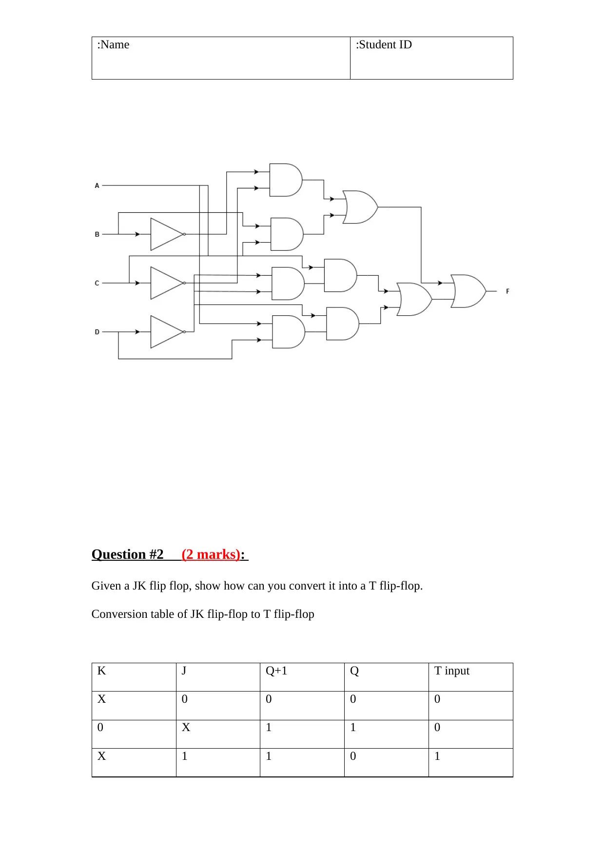
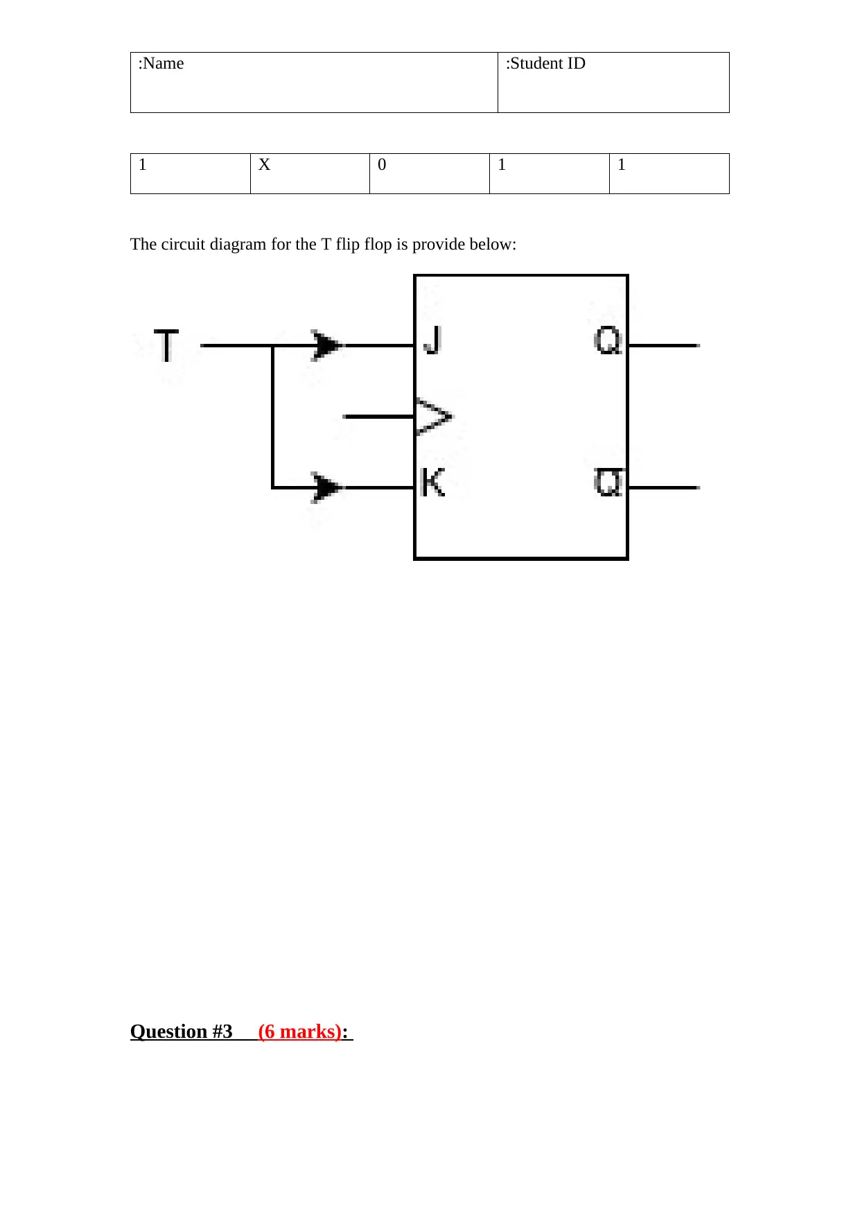
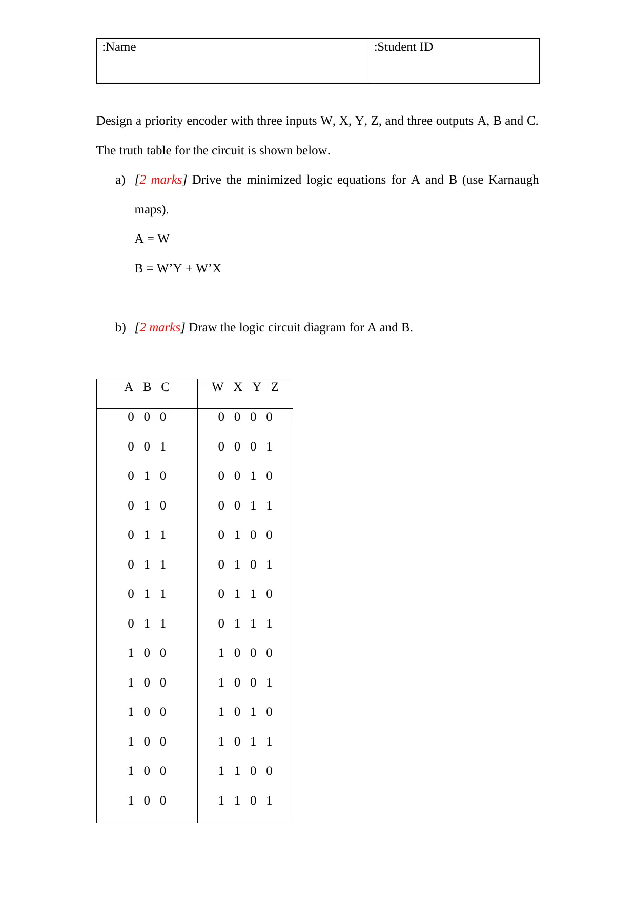
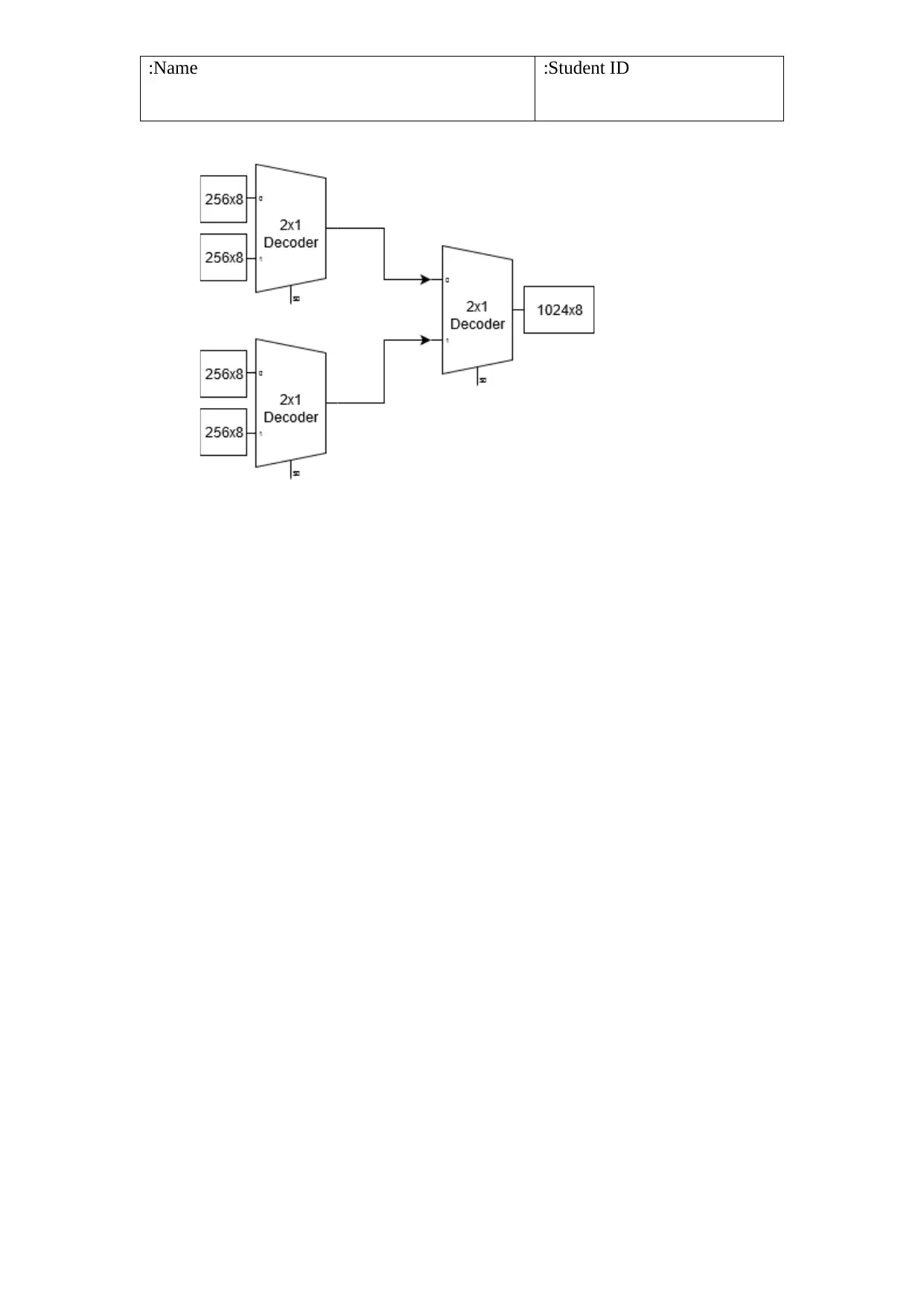
This document provides a comprehensive solution to Homework 1 for the Computer Architecture and Organization I (CMPE 263) course. The assignment covers fundamental concepts in digital logic and circuit design. The solution includes the simplification of Boolean functions using Karnaugh maps and the design of logic diagrams with AND-OR gates. It also details the conversion of a JK flip-flop to a T flip-flop, and the design of a priority encoder. The solution further addresses sequential circuits, including writing logic functions and determining the next state of flip-flops. Additionally, the assignment involves problems related to shift registers, multiplexer construction, and ROM memory design, including calculating the number of chips, address lines, and decoder size required for memory implementation.
tabler-icon-diamond-filled.svg

Contribute Materials

Your contribution can guide someone’s learning journey. Share your documents today.
Document Page
Student ID:Name:
Computer Architecture and
Organization I
CMPE 263
Spring 2020
Dept. of Computer Science and
Engineering
College of Engineering
Qatar University
Homework #1 – Spring 2020
Digital Logic Circuit and Digital Components
Please submit a hardcopy by Wednesday January 29, 2020
Question #1 (4 marks):
Given the Boolean function:
F (A , B , C , D)= m(0,1 , 4 ,6 , 7 , 8 , 9 ,13 ,14,15)
1) [2 marks] Drive the simplified Boolean function in sum-of-products form by
means of a four-variable Karnaugh map.
F (A, B, C, D) = B'C' + BC + A'C'D' + AC'D
2) [2 marks] Draw the logic diagram with AND-OR gates.
tabler-icon-diamond-filled.svg

Secure Best Marks with AI Grader

Need help grading? Try our AI Grader for instant feedback on your assignments.
Document Page
Student ID:Name:
Question #2 (2 marks):
Given a JK flip flop, show how can you convert it into a T flip-flop.
Conversion table of JK flip-flop to T flip-flop
T inputQQ+1JK
0000X
011X0
1011X
Document Page
Student ID:Name:
110X1
The circuit diagram for the T flip flop is provide below:
Question #3 (6 marks):
Document Page
Student ID:Name:
Design a priority encoder with three inputs W, X, Y, Z, and three outputs A, B and C.
The truth table for the circuit is shown below.
a) [2 marks] Drive the minimized logic equations for A and B (use Karnaugh
maps).
A = W
B = W’Y + W’X
b) [2 marks] Draw the logic circuit diagram for A and B.
W X Y ZA B C
0 0 0 0
0 0 0 1
0 0 1 0
0 0 1 1
0 1 0 0
0 1 0 1
0 1 1 0
0 1 1 1
1 0 0 0
1 0 0 1
1 0 1 0
1 0 1 1
1 1 0 0
1 1 0 1
0 0 0
0 0 1
0 1 0
0 1 0
0 1 1
0 1 1
0 1 1
0 1 1
1 0 0
1 0 0
1 0 0
1 0 0
1 0 0
1 0 0
tabler-icon-diamond-filled.svg

Secure Best Marks with AI Grader

Need help grading? Try our AI Grader for instant feedback on your assignments.
Document Page
Student ID:Name:
1 1 1 0
1 1 1 1
1 0 0
1 0 0
Question #4 (6 mark):
Given a sequential circuit (shown in the figure below) that has two T flip-flops A and
B, two inputs X and Y, and one output Z.
a) [2 marks] Write the logic function for the flip-flops inputs TA and TB, as a
function of X, Y, A and B.
TA = (X+A) (X’+Y)
TB = (Y+B) (X’+B)
b) [1 mark] Write the logic function for the output Z as a function of A and B.
Z = A’+B
c) [3 marks] If the present state of A and B are A = 0 and B = 0, and the circuit
inputs are X = 1 and Y = 1.
Then, what will be the next state values for the flip-flops A and B?
Document Page
Student ID:Name:
What will be the value of output Z, in this case?
A = 1, B = 0, Z = 0
Question #5 (3 marks):
The content of a 4-bit register is initially 1001. The register is shifted six times to the
right, with the serial input (SI) being 010010. What is the content of the register after
each shift?
Document Page
Student ID:Name:
Q3 Q2 Q1 Q0
Initial content of register1 0 0 1
Content after first shift0 0 1 0
Content after second shift0 1 0 1
Content after third shift1 0 10
Content after fourth shift0 1 0 0
Content after fifth shift1 0 0 1
Content after sixth shift0 0 1 0
Question #6 (3 marks):
Construct a 16-to-1 line multiplexer with two 8-to-1 line multiplexers and one 2-to-1
line multiplexer. Use block diagrams for the three multiplexers.
tabler-icon-diamond-filled.svg

Paraphrase This Document

Need a fresh take? Get an instant paraphrase of this document with our AI Paraphraser
Document Page
Student ID:Name:
Document Page
Student ID:Name:
Question #7 (6 marks):
Construct a ROM memory with the size 1024 x 8 ROM, knowing that in the lab, you
only have ROM chips with the size of 256 x 8 chips with an enable input. You can
construct the memory with the given chips and a decoder.
a) [1 mark] How many ROM chips are needed to construct the required
memory?
4 ROM chips are needed to construct the required memory
b) [1 mark] How many address lines are needed for the required memory?
There 10 address lines in the require memory.
c) [1 mark] How many address lines in one chip?
There are 8 address lines in one chip.
d) [1 mark] What is the size of the decoder used? (number of inputs and outputs)
3 2x1 decoders can be used here.
e) [2 mark] Draw the organization of the constructed memory, showing the
external connections necessary to construct the required memory.
Document Page
Student ID:Name:
chevron_up_icon
1 out of 10
circle_padding
hide_on_mobile
zoom_out_icon
logo.png

Your All-in-One AI-Powered Toolkit for Academic Success.

Available 24*7 on WhatsApp / Email

[object Object]