Detailed Design Report: Buck-Boost DC-DC Converter Analysis
VerifiedAdded on 2023/06/15
|35
|7113
|252
Report
AI Summary
This report presents a detailed design of a buck-boost DC-DC converter, a versatile topology combining buck and boost functionalities for voltage regulation. The report covers the converter's operation in both continuous and discontinuous conduction modes, providing in-depth analysis of each. Design specifications, including input voltage range, output voltage, and current requirements, are outlined. The design process encompasses the calculation of the duty cycle, selection of appropriate inductor and capacitor values, determination of maximum switching current, and output voltage setting. Furthermore, the report discusses MOSFET selection criteria for the converter and includes a design evaluation section, explaining the circuit's operation and performance. The design is simulated using Multisim software, and simulation results are presented to validate the design.

Design of a buck-boost DC-DC Converter 1
DESIGN OF A BUCK BOOST DC-DC CONVERTER
1
DESIGN OF A BUCK BOOST DC-DC CONVERTER
1
Paraphrase This Document
Need a fresh take? Get an instant paraphrase of this document with our AI Paraphraser
Design of a buck-boost DC-DC Converter 2
SUMMARY
For a switching power supply, it is composed of the control circuit and power stage. The
power stages carry out the key power conversion to the output voltage from the input supply and
this constitutes the filter at the output and switches. This design report will basically focus on the
design of buck-boost converter for switched mode power supply. The in-depth operation of this
DC-DC converter works in both discontinuous and continuous mode which will actually be
shown in this article.
2

Design of a buck-boost DC-DC Converter 3
TABLE OF CONTENTS
ACKNOWLEDGMENTS...............................................................................................................2
SUMMARY.....................................................................................................................................2
INTRODUCTION...........................................................................................................................6
Buck-Boost Converters....................................................................................................................6
Schematic diagram of the buck-boost converter..........................................................................7
Buck-Boost Steady-State Continuous Conduction Mode Analysis...........................................11
Buck-Boost Steady-State discontinuous Conduction Mode Analysis.......................................13
SPECIFICATION..........................................................................................................................14
DESIGN PARAMETERS.............................................................................................................15
DESCRIPTION OF DESIGN........................................................................................................15
Calculation of the Duty Cycle....................................................................................................15
Buck mode.................................................................................................................................16
Boost mode................................................................................................................................16
Selection of input capacitor........................................................................................................17
Selection of output capacitor......................................................................................................17
Inductor Selection......................................................................................................................18
Buck Mode.................................................................................................................................18
Boost mode................................................................................................................................19
Calculation of maximum switching current...............................................................................19
Buck Mode.................................................................................................................................19
Boost Mode................................................................................................................................20
Output voltage setting................................................................................................................ 21
MOSFET selection for the Buck-boost converter......................................................................22
3
⊘ This is a preview!⊘
Do you want full access?
Subscribe today to unlock all pages.
Trusted by 1+ million students worldwide

Design of a buck-boost DC-DC Converter 4
Design evaluation.......................................................................................................................24
Explanation of the operation of the above design..................................................................24
DISCUSSION…………………………………………………………………………………... 26
CONCLUSION…………………………………………………………………………………. 28
REFERENCES…………………………………………………………………………………. 29
APPENDICES…………………………………………………………………………………. 30
4
Paraphrase This Document
Need a fresh take? Get an instant paraphrase of this document with our AI Paraphraser
Design of a buck-boost DC-DC Converter 5
List of Figures
Fig 1: Block diagram of DC/DC regulator.....................................................................................5
Fig 2: Buck-Boost Power Stage Schematic.....................................................................................6
Fig 3: Buck-Boost Power Stage Schematic from multism..............................................................6
Fig 3: Buck-Boost Power Stage Schematic from multism..............................................................7
Fig 4: Showing Continuous Mode Buck-Boost Power Stage Waveforms......................................8
Fig 5: Showing discontinuous Current Mode..................................................................................9
Fig 6: Showing the Buck-boost converter showing the output voltage.........................................16
Fig 7: Showing the Buck-boost converter showing the output current.........................................16
Fig 8: Showing the waveform of the buck-boost DC/DC converter.............................................17
5
Design of a buck-boost DC-DC Converter 6
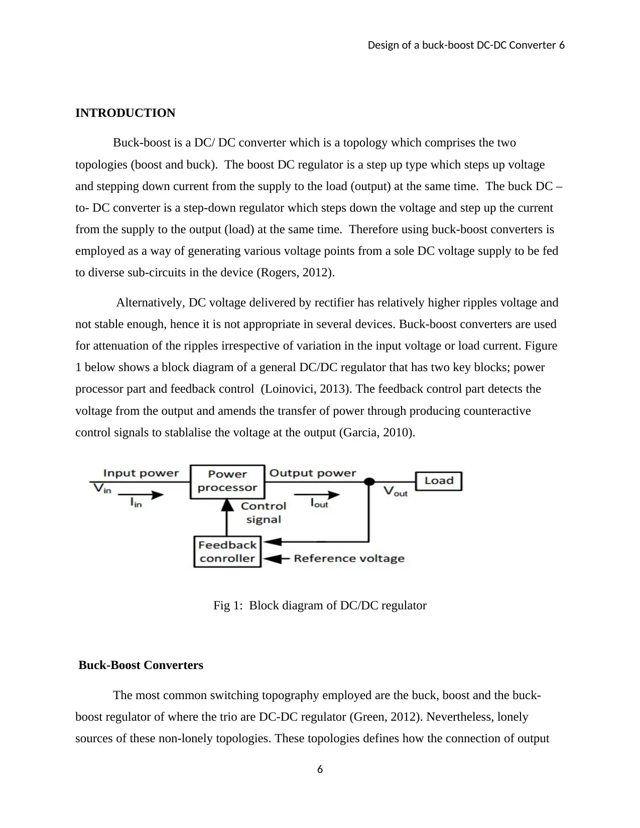
INTRODUCTION
Buck-boost is a DC/ DC converter which is a topology which comprises the two
topologies (boost and buck). The boost DC regulator is a step up type which steps up voltage
and stepping down current from the supply to the load (output) at the same time. The buck DC –
to- DC converter is a step-down regulator which steps down the voltage and step up the current
from the supply to the output (load) at the same time. Therefore using buck-boost converters is
employed as a way of generating various voltage points from a sole DC voltage supply to be fed
to diverse sub-circuits in the device (Rogers, 2012).
Alternatively, DC voltage delivered by rectifier has relatively higher ripples voltage and
not stable enough, hence it is not appropriate in several devices. Buck-boost converters are used
for attenuation of the ripples irrespective of variation in the input voltage or load current. Figure
1 below shows a block diagram of a general DC/DC regulator that has two key blocks; power
processor part and feedback control (Loinovici, 2013). The feedback control part detects the
voltage from the output and amends the transfer of power through producing counteractive
control signals to stablalise the voltage at the output (Garcia, 2010).
Fig 1: Block diagram of DC/DC regulator
Buck-Boost Converters
The most common switching topography employed are the buck, boost and the buck-
boost regulator of where the trio are DC-DC regulator (Green, 2012). Nevertheless, lonely
sources of these non-lonely topologies. These topologies defines how the connection of output
6
⊘ This is a preview!⊘
Do you want full access?
Subscribe today to unlock all pages.
Trusted by 1+ million students worldwide
Design of a buck-boost DC-DC Converter 7
inductor, switches, and output capacitor are done (Silva, 2016). Apiece topology has exceptional
stuffs. These comprise conversion the stable-state voltage ratios, the chatracter of the output and
input currents, and the properties of the output voltage ripple (Xi, 2012) . Electronic engineers
select the buck-boost power stage since the voltage at the output is reversed from the output and
input voltage can be either lower or higher than the voltage at the input (Kennedy, 2013). The
topology acquires its appellation from generating a voltage at the output which can be (buck
power stage) or lower (boost power stage) in amount than the voltage at the input (Siu, 2011).
Nonetheless, the voltage at the output is reversed in polarity from the input voltage (Hauke,
2011).
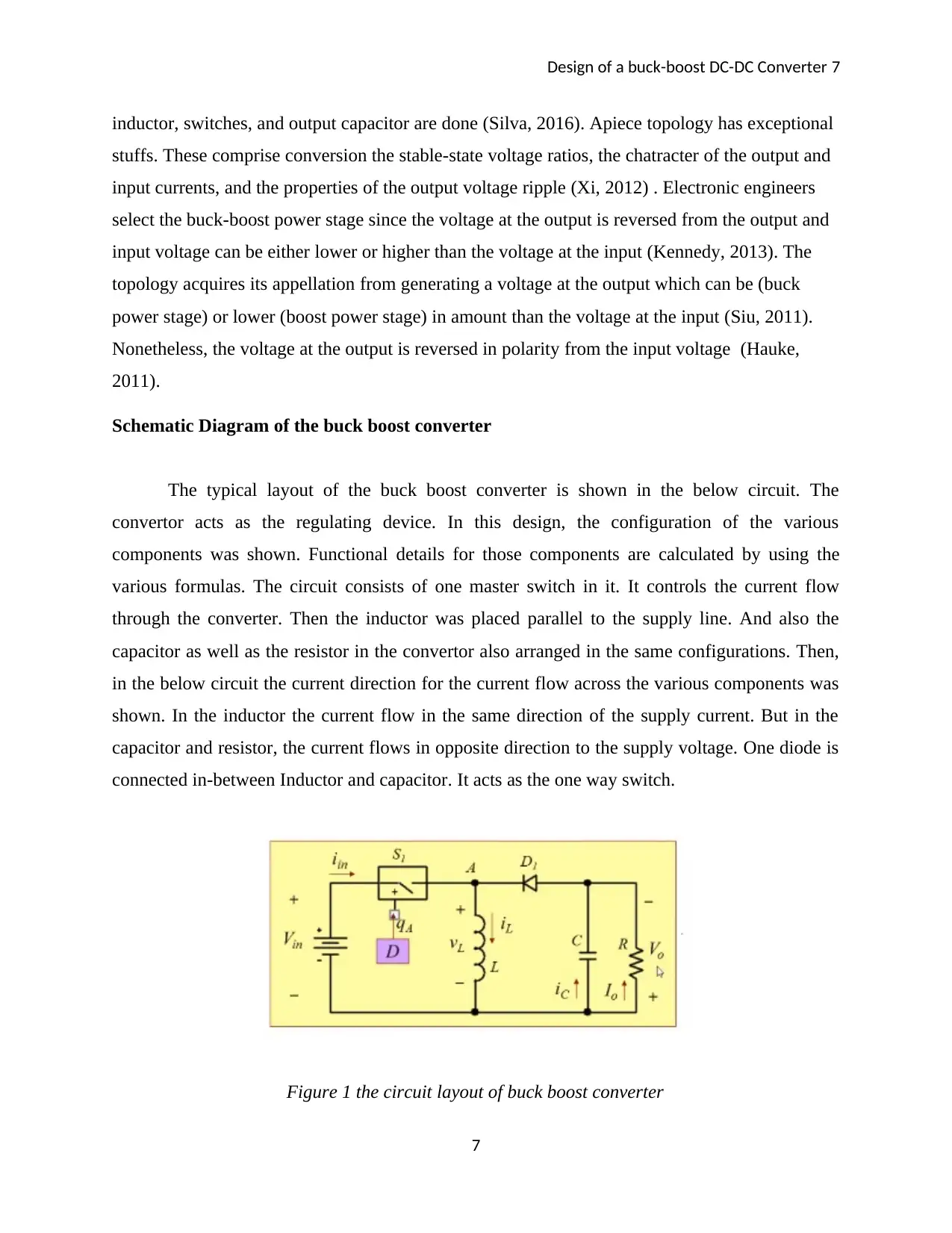
Schematic Diagram of the buck boost converter
The typical layout of the buck boost converter is shown in the below circuit. The
convertor acts as the regulating device. In this design, the configuration of the various
components was shown. Functional details for those components are calculated by using the
various formulas. The circuit consists of one master switch in it. It controls the current flow
through the converter. Then the inductor was placed parallel to the supply line. And also the
capacitor as well as the resistor in the convertor also arranged in the same configurations. Then,
in the below circuit the current direction for the current flow across the various components was
shown. In the inductor the current flow in the same direction of the supply current. But in the
capacitor and resistor, the current flows in opposite direction to the supply voltage. One diode is
connected in-between Inductor and capacitor. It acts as the one way switch.
Figure 1 the circuit layout of buck boost converter
7
inductor, switches, and output capacitor are done (Silva, 2016). Apiece topology has exceptional
stuffs. These comprise conversion the stable-state voltage ratios, the chatracter of the output and
input currents, and the properties of the output voltage ripple (Xi, 2012) . Electronic engineers
select the buck-boost power stage since the voltage at the output is reversed from the output and
input voltage can be either lower or higher than the voltage at the input (Kennedy, 2013). The
topology acquires its appellation from generating a voltage at the output which can be (buck
power stage) or lower (boost power stage) in amount than the voltage at the input (Siu, 2011).
Nonetheless, the voltage at the output is reversed in polarity from the input voltage (Hauke,
2011).
Schematic Diagram of the buck boost converter
The typical layout of the buck boost converter is shown in the below circuit. The
convertor acts as the regulating device. In this design, the configuration of the various
components was shown. Functional details for those components are calculated by using the
various formulas. The circuit consists of one master switch in it. It controls the current flow
through the converter. Then the inductor was placed parallel to the supply line. And also the
capacitor as well as the resistor in the convertor also arranged in the same configurations. Then,
in the below circuit the current direction for the current flow across the various components was
shown. In the inductor the current flow in the same direction of the supply current. But in the
capacitor and resistor, the current flows in opposite direction to the supply voltage. One diode is
connected in-between Inductor and capacitor. It acts as the one way switch.
Figure 1 the circuit layout of buck boost converter
7
Paraphrase This Document
Need a fresh take? Get an instant paraphrase of this document with our AI Paraphraser

Design of a buck-boost DC-DC Converter 8
Switch closed state
When the switch is closed, then the current will not flow directly to the diode. The
current first flows through the inductor L, then to the capacitor C, and Resistor R. In this stage
the diode is in reverse biased state. The current through the inductor is represented as iL, the
current through the capacitor is iC, and the output current Io is measured across resistor R. The
input voltage is represented as Vin and Output voltage is represented as Vo. When the switch is
in ON condition, the inductor voltage equals to the Input voltage. Then the energy is stored in an
Inductor gets increases. Then the capacitor maintains the constant voltage.
Here, q= 1 switch –ON = Diode Reverse biased.
Figure 2 the circuit in closed switch state
Switch open state
The below figure consists of a closed switch circuit of the buck-boost converter. When
the switch is in OFF condition, the inductor voltage equals to the negative value of Output
voltage. Then the energy is stored in an Inductor gets decreases. Then the capacitor maintains
the constant voltage. In the open state of the switch, the current flows through the Inductor,
capacitor, and resistor. The flow of current is shown in below circuit. In this stage, the diode is
forward biased.
Here q=0 switch – off = Diode forward biased
8
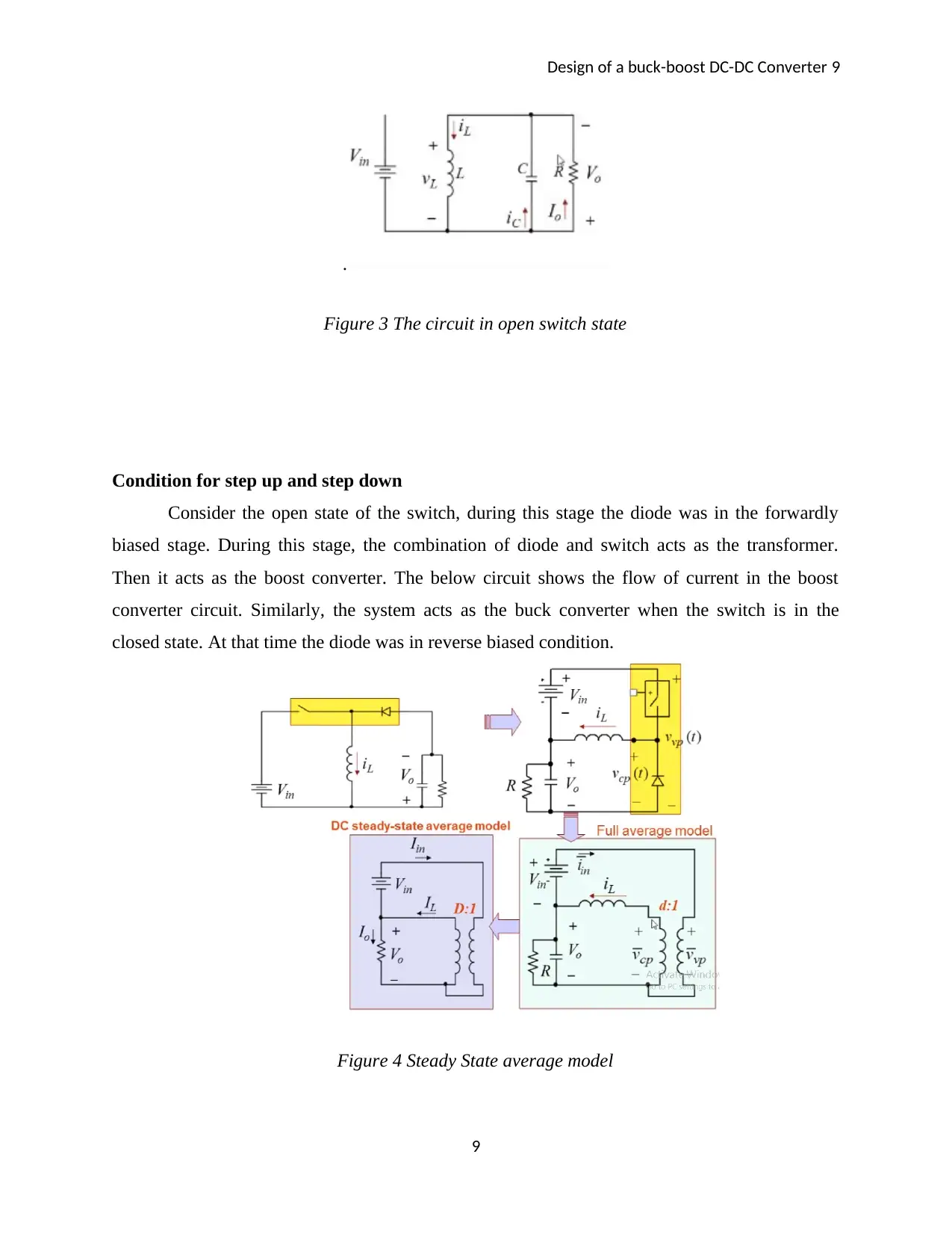
Design of a buck-boost DC-DC Converter 9
.
Figure 3 The circuit in open switch state
Condition for step up and step down
Consider the open state of the switch, during this stage the diode was in the forwardly
biased stage. During this stage, the combination of diode and switch acts as the transformer.
Then it acts as the boost converter. The below circuit shows the flow of current in the boost
converter circuit. Similarly, the system acts as the buck converter when the switch is in the
closed state. At that time the diode was in reverse biased condition.
Figure 4 Steady State average model
9
⊘ This is a preview!⊘
Do you want full access?
Subscribe today to unlock all pages.
Trusted by 1+ million students worldwide

Design of a buck-boost DC-DC Converter 10
Schematic representation of a basic Buck Boost Converter
The basic configuration of buck boost converter is shown in below diagram. In which the
switches are acts as MOSFET(Metal Oxide Semiconductor Field Efffect transistor). It consists of
one inductor,two capacitors and four switches.This kind of converters reduce size of the solution
and the difficulty of the solution tends to become easy.
Figure 5 Schematic layout of basic Buck Boost converter
Power stage parameters of Buck Boost converter
The important parameters used to calculate the power stage are in the following:
1. Maximum output current (Iout)
2. Range of input voltage (Vin min and Vin max)
3. Desired output voltage (Vout)
The above-mentioned parameters are needed to calculate the analysis of buck-boost
converter.Buck-boost converter was built with the help of Integrator circuit. For calculation
purpose, some constant parameters are taken from the datasheet. The power stage can be
calculated easily after the four parameters are obtained.
When the above figure two was drawn in the multism the below circuit diagram is obtained.
10
Paraphrase This Document
Need a fresh take? Get an instant paraphrase of this document with our AI Paraphraser

Design of a buck-boost DC-DC Converter 11
Fig 3: Buck-Boost Power Stage Schematic from multism
Fig 3: Buck-Boost Power Stage Schematic from multism
The output voltage must be kept stable, irrespective of vicissitudes in the input voltage/load
current (James, 2013). This is achieved by building a feedback circuit which vicissitudes the
converter control input in such a way that the difference between output voltage and anticipated
reference value must be minimalized.
Buck-Boost Steady-State Continuous Conduction Mode Analysis
The time for the switching to be in ON state is given as
TON = D × TS . . . . . . . . . . . . . . . . . . . . . . . . . . . . . . . . . . . . . . . . . . . . . . . . . . . . . . . . . . . . 1
11
Fig 3: Buck-Boost Power Stage Schematic from multism
Fig 3: Buck-Boost Power Stage Schematic from multism
The output voltage must be kept stable, irrespective of vicissitudes in the input voltage/load
current (James, 2013). This is achieved by building a feedback circuit which vicissitudes the
converter control input in such a way that the difference between output voltage and anticipated
reference value must be minimalized.
Buck-Boost Steady-State Continuous Conduction Mode Analysis
The time for the switching to be in ON state is given as
TON = D × TS . . . . . . . . . . . . . . . . . . . . . . . . . . . . . . . . . . . . . . . . . . . . . . . . . . . . . . . . . . . . 1
11

Design of a buck-boost DC-DC Converter 12
Where D is the duty cycle
The time for the switching to be in ON state is known as TOFF. Because there are only two
states per switching cycle for continuous conduction mode (Nteilele, 2012). TOFF will be given
by the following equation
TOFF = (1−D) × TS . . . . . . . . . . . . . . . . . . . . . . . . . . . . . . . . . . . . . . . . . . . . . . . . . . . . . . . . . . . . 2
Where (1−D) is known as called D’.
And the summation of TON and TOFF is known as the settling time.
And the graphs for the TON and TOFF are shown in the following figures
12
⊘ This is a preview!⊘
Do you want full access?
Subscribe today to unlock all pages.
Trusted by 1+ million students worldwide
1 out of 35
Related Documents


Your All-in-One AI-Powered Toolkit for Academic Success.
+13062052269
info@desklib.com
Available 24*7 on WhatsApp / Email
![[object Object]](/_next/static/media/star-bottom.7253800d.svg)
Unlock your academic potential
Copyright © 2020–2026 A2Z Services. All Rights Reserved. Developed and managed by ZUCOL.