Digital Communication Systems Lab Report: PCM, ASK, and Demodulation
VerifiedAdded on 2021/04/16
|25
|3898
|171
Practical Assignment
AI Summary
This lab report details experiments on digital communication systems, focusing on Pulse Code Modulation (PCM) and Amplitude Shift Keying (ASK) techniques. The report covers the implementation of PCM encoding and decoding, including the use of low-pass filters and the generation of sine waves. It also explores ASK modulation and demodulation, comparing signal characteristics and addressing practical considerations such as noise effects. The experiments involve setting up PCM encoders and decoders, generating and demodulating ASK signals, and analyzing the impact of noise on signal transmission. The report answers experiment questions related to the PCM encoder's output, binary number changes, and the challenges of obtaining specific voltage levels. It also discusses methods for obtaining variable DC voltages and their impact on the system. The objective is to develop an understanding of digital communication systems and their practical applications.
DIGITAL COMMUNICATION SYSTEM
BY
AFFILIATE
BY
AFFILIATE
Paraphrase This Document
Need a fresh take? Get an instant paraphrase of this document with our AI Paraphraser
Contents
I.0 INTRODUCTION....................................................................................................................2
1.1 OBJECTIVE.........................................................................................................................2
2.0 SESSION IMPLEMENTATIONS.........................................................................................2
2.1 PULSE CODE MODULATION.........................................................................................2
2.1.1 Low Pass Filter................................................................................................................3
2.1.2 Decoder...........................................................................................................................3
2.1.3 Setting up PCM encoder..................................................................................................4
2.1.4 Setting up PCM decoding................................................................................................5
2.1.4 PCM Sine Wave.............................................................................................................6
2.1.6 Sound form PCM Decoder...........................................................................................7
2.1.7 The PCM headphone.....................................................................................................8
2.2 THE AMPLITUDE SHIFT KEYING................................................................................8
2.2.1 Demodulating ASK........................................................................................................9
2.2.2 Comparing the signal ASK.........................................................................................10
3.0 EXPERIMENT QUESTIONS..............................................................................................12
3.1 Experiment 12: PCM Encoding.......................................................................................12
3.2 Experiment 13: PCM Decoding.......................................................................................14
3.3 EXPERIMENT 10: AMPLITUDE SHIFT KEYING DEMODULATION..................15
3.3.1 Part A: Generating an ASK signal................................................................................15
3.3.2 PART B: Demodulating an ASK Signal.......................................................................16
3.3.3 PART C: Restoring the Recovered Digital Signal using Comparator..........................16
3.4 Experiment 11: ASK Demodulation Using Product Detection......................................18
4.0 CONCLUSION.....................................................................................................................19
REFERENCES............................................................................................................................20
I.0 INTRODUCTION
Digital communication system is a method of correspondence where the data or the thinking is
encoded carefully as circumspect signs and electronically exchanged to the beneficiaries. Digital
communication system is a standout amongst the most normally utilized method of
communication in the present situation. Associations by and large depend on this mode for all
their business communication.
Currently, the digital communication is taking over from the analog systems of communication ,
a good example of the situation where the digital systems have taken over the analog systems is
the telecommunication channel. It is therefore very important and better to have a good know
how of the digital communication systems. For the communication to be termed complete, there
must pass through a medium. The channel must be there for the communication to be complete,
or even for the communication to take place. This is not limited to the kind of channel the
communication uses, this might be optical fiber cables, free spaces or even the copper wire.
Assuming that the channel is not shared as required, then transmission of information could only
take place in a single one direction creating a lot of shortcomings when it comes to
communication.
The time division multiplexing is one of the method that is used for sharing channel, this method
involves allowing the user to have full access to the channel though the period that the user has
been allowed is very short.
⊘ This is a preview!⊘
Do you want full access?
Subscribe today to unlock all pages.
Trusted by 1+ million students worldwide
Another method is the frequency division multiplexing, which involves allowing use to have
uninterrupted time with the channel for as long time period.
1.1 OBJECTIVE
The main objective of this session is to develop a digital communication systems that are
effective and efficient enough to completely take over the analog systems of communication.
2.0 SESSION IMPLEMENTATIONS
2.1 PULSE CODE MODULATION
This is a system that is used to encode the analog system to a 0s and 1s stream. This PCM
encoder uses the codec in changing the analog voltage that is in between the -2 and the +2 into
an 8 bit binary numbers.
2.1.1 Low Pass Filter
This kind of channel expels all high recurrence components that are inside the information
simple analog signal which is more noteworthy than the most astounding recurrence of the
message motion, to abstain from associating of the message signal. The figure below shows how
low pass filter works.
Paraphrase This Document
Need a fresh take? Get an instant paraphrase of this document with our AI Paraphraser
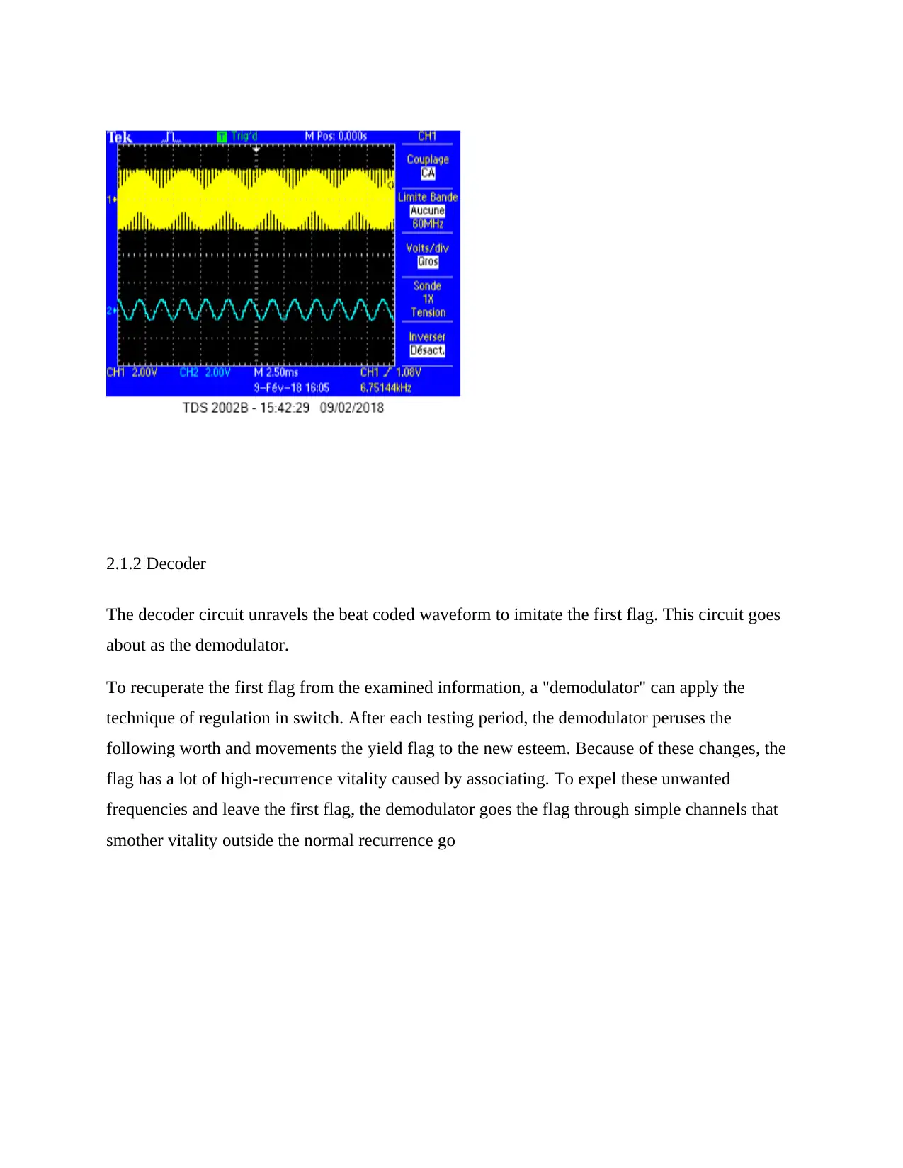
2.1.2 Decoder
The decoder circuit unravels the beat coded waveform to imitate the first flag. This circuit goes
about as the demodulator.
To recuperate the first flag from the examined information, a "demodulator" can apply the
technique of regulation in switch. After each testing period, the demodulator peruses the
following worth and movements the yield flag to the new esteem. Because of these changes, the
flag has a lot of high-recurrence vitality caused by associating. To expel these unwanted
frequencies and leave the first flag, the demodulator goes the flag through simple channels that
smother vitality outside the normal recurrence go
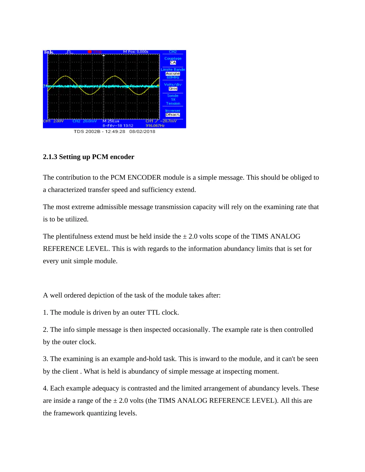
2.1.3 Setting up PCM encoder
The contribution to the PCM ENCODER module is a simple message. This should be obliged to
a characterized transfer speed and sufficiency extend.
The most extreme admissible message transmission capacity will rely on the examining rate that
is to be utilized.
The plentifulness extend must be held inside the ± 2.0 volts scope of the TIMS ANALOG
REFERENCE LEVEL. This is with regards to the information abundancy limits that is set for
every unit simple module.
A well ordered depiction of the task of the module takes after:
1. The module is driven by an outer TTL clock.
2. The info simple message is then inspected occasionally. The example rate is then controlled
by the outer clock.
3. The examining is an example and-hold task. This is inward to the module, and it can't be seen
by the client . What is held is abundancy of simple message at inspecting moment.
4. Each example adequacy is contrasted and the limited arrangement of abundancy levels. These
are inside a range of the ± 2.0 volts (the TIMS ANALOG REFERENCE LEVEL). All this are
the framework quantizing levels.
⊘ This is a preview!⊘
Do you want full access?
Subscribe today to unlock all pages.
Trusted by 1+ million students worldwide
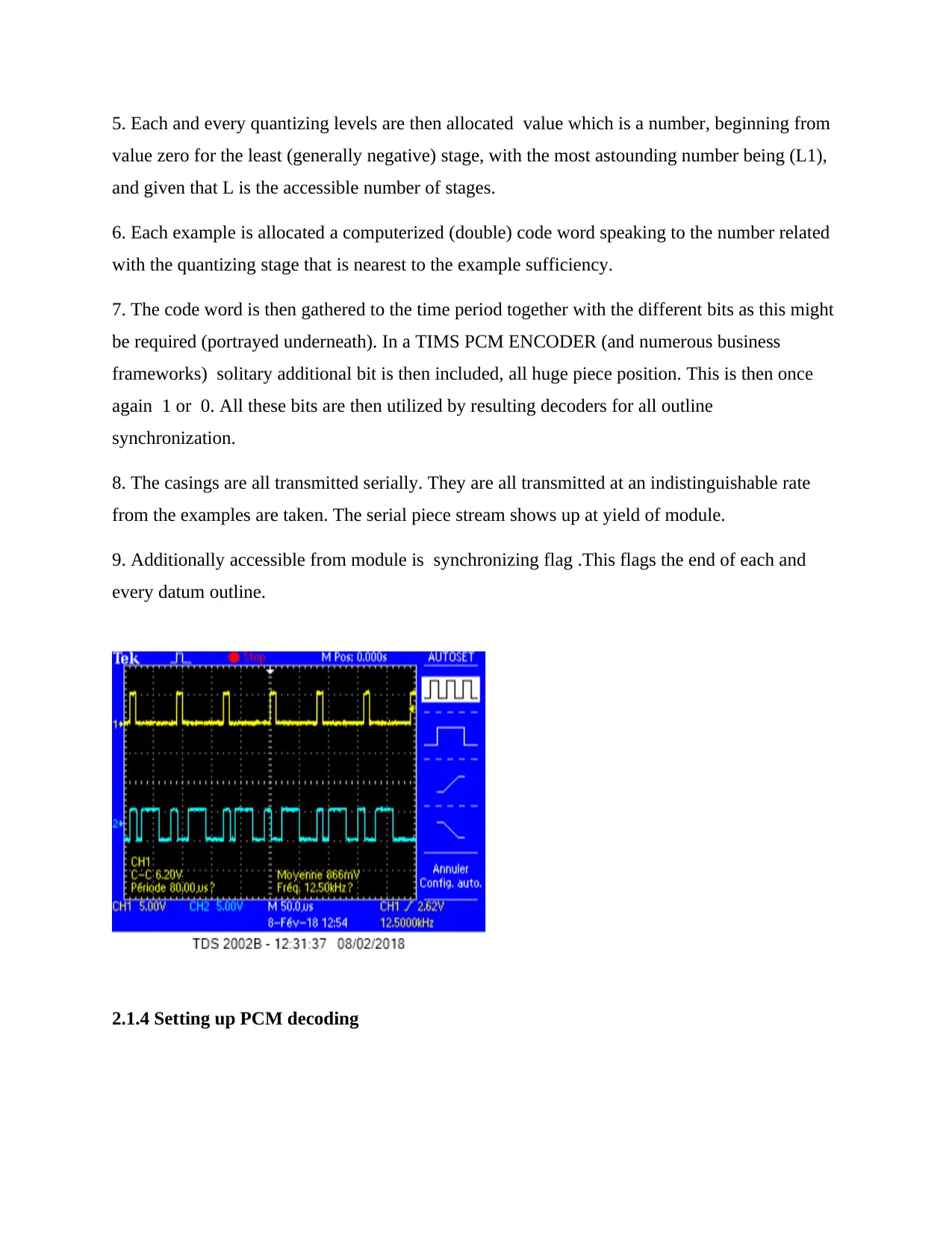
5. Each and every quantizing levels are then allocated value which is a number, beginning from
value zero for the least (generally negative) stage, with the most astounding number being (L1),
and given that L is the accessible number of stages.
6. Each example is allocated a computerized (double) code word speaking to the number related
with the quantizing stage that is nearest to the example sufficiency.
7. The code word is then gathered to the time period together with the different bits as this might
be required (portrayed underneath). In a TIMS PCM ENCODER (and numerous business
frameworks) solitary additional bit is then included, all huge piece position. This is then once
again 1 or 0. All these bits are then utilized by resulting decoders for all outline
synchronization.
8. The casings are all transmitted serially. They are all transmitted at an indistinguishable rate
from the examples are taken. The serial piece stream shows up at yield of module.
9. Additionally accessible from module is synchronizing flag .This flags the end of each and
every datum outline.
2.1.4 Setting up PCM decoding
Paraphrase This Document
Need a fresh take? Get an instant paraphrase of this document with our AI Paraphraser
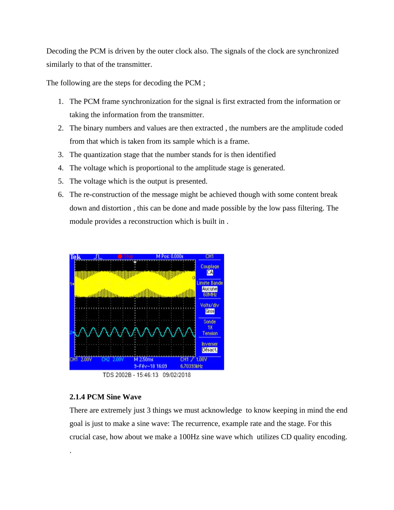
Decoding the PCM is driven by the outer clock also. The signals of the clock are synchronized
similarly to that of the transmitter.
The following are the steps for decoding the PCM ;
1. The PCM frame synchronization for the signal is first extracted from the information or
taking the information from the transmitter.
2. The binary numbers and values are then extracted , the numbers are the amplitude coded
from that which is taken from its sample which is a frame.
3. The quantization stage that the number stands for is then identified
4. The voltage which is proportional to the amplitude stage is generated.
5. The voltage which is the output is presented.
6. The re-construction of the message might be achieved though with some content break
down and distortion , this can be done and made possible by the low pass filtering. The
module provides a reconstruction which is built in .
2.1.4 PCM Sine Wave
There are extremely just 3 things we must acknowledge to know keeping in mind the end
goal is just to make a sine wave: The recurrence, example rate and the stage. For this
crucial case, how about we make a 100Hz sine wave which utilizes CD quality encoding.
.
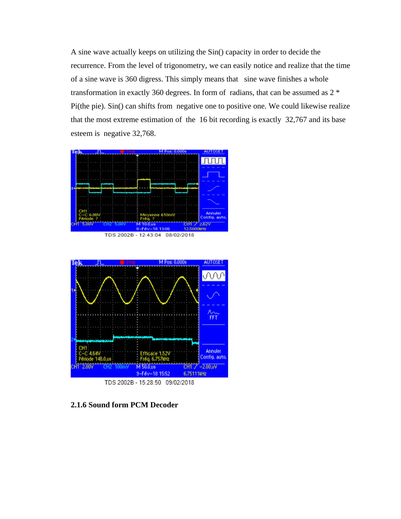
A sine wave actually keeps on utilizing the Sin() capacity in order to decide the
recurrence. From the level of trigonometry, we can easily notice and realize that the time
of a sine wave is 360 digress. This simply means that sine wave finishes a whole
transformation in exactly 360 degrees. In form of radians, that can be assumed as 2 *
Pi(the pie). Sin() can shifts from negative one to positive one. We could likewise realize
that the most extreme estimation of the 16 bit recording is exactly 32,767 and its base
esteem is negative 32,768.
2.1.6 Sound form PCM Decoder
⊘ This is a preview!⊘
Do you want full access?
Subscribe today to unlock all pages.
Trusted by 1+ million students worldwide
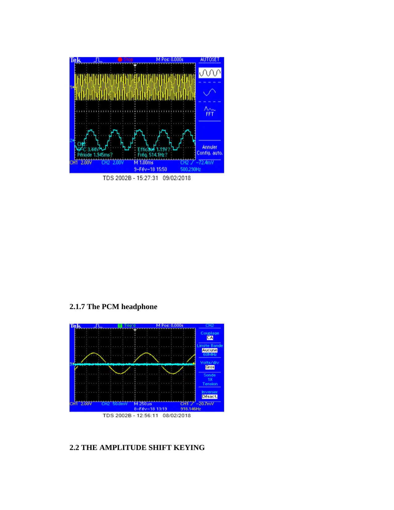
2.1.7 The PCM headphone
2.2 THE AMPLITUDE SHIFT KEYING
2.2 THE AMPLITUDE SHIFT KEYING
Paraphrase This Document
Need a fresh take? Get an instant paraphrase of this document with our AI Paraphraser
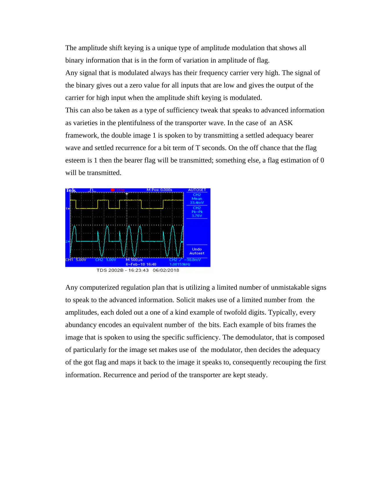
The amplitude shift keying is a unique type of amplitude modulation that shows all
binary information that is in the form of variation in amplitude of flag.
Any signal that is modulated always has their frequency carrier very high. The signal of
the binary gives out a zero value for all inputs that are low and gives the output of the
carrier for high input when the amplitude shift keying is modulated.
This can also be taken as a type of sufficiency tweak that speaks to advanced information
as varieties in the plentifulness of the transporter wave. In the case of an ASK
framework, the double image 1 is spoken to by transmitting a settled adequacy bearer
wave and settled recurrence for a bit term of T seconds. On the off chance that the flag
esteem is 1 then the bearer flag will be transmitted; something else, a flag estimation of 0
will be transmitted.
Any computerized regulation plan that is utilizing a limited number of unmistakable signs
to speak to the advanced information. Solicit makes use of a limited number from the
amplitudes, each doled out a one of a kind example of twofold digits. Typically, every
abundancy encodes an equivalent number of the bits. Each example of bits frames the
image that is spoken to using the specific sufficiency. The demodulator, that is composed
of particularly for the image set makes use of the modulator, then decides the adequacy
of the got flag and maps it back to the image it speaks to, consequently recouping the first
information. Recurrence and period of the transporter are kept steady.
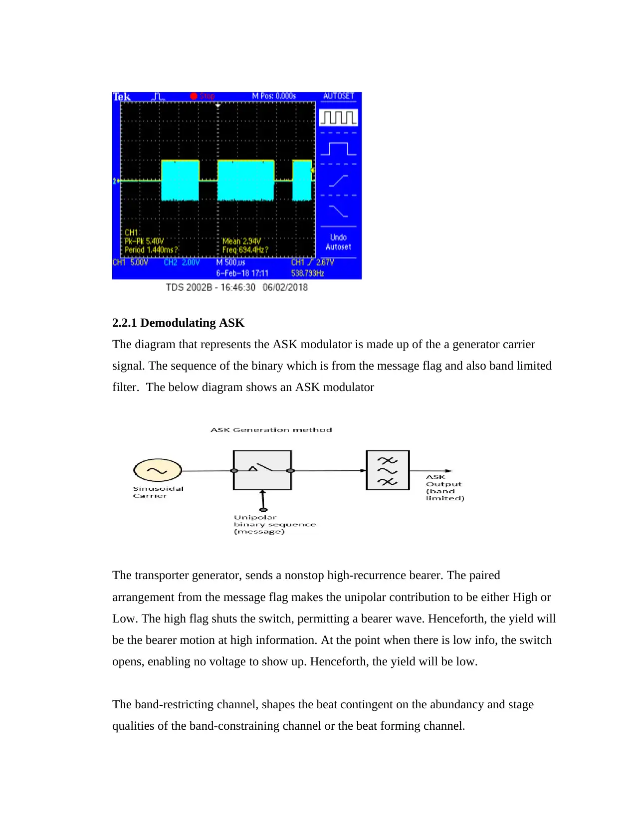
2.2.1 Demodulating ASK
The diagram that represents the ASK modulator is made up of the a generator carrier
signal. The sequence of the binary which is from the message flag and also band limited
filter. The below diagram shows an ASK modulator
The transporter generator, sends a nonstop high-recurrence bearer. The paired
arrangement from the message flag makes the unipolar contribution to be either High or
Low. The high flag shuts the switch, permitting a bearer wave. Henceforth, the yield will
be the bearer motion at high information. At the point when there is low info, the switch
opens, enabling no voltage to show up. Henceforth, the yield will be low.
The band-restricting channel, shapes the beat contingent on the abundancy and stage
qualities of the band-constraining channel or the beat forming channel.
⊘ This is a preview!⊘
Do you want full access?
Subscribe today to unlock all pages.
Trusted by 1+ million students worldwide
1 out of 25
Related Documents


Your All-in-One AI-Powered Toolkit for Academic Success.
+13062052269
info@desklib.com
Available 24*7 on WhatsApp / Email
![[object Object]](/_next/static/media/star-bottom.7253800d.svg)
Unlock your academic potential
Copyright © 2020–2026 A2Z Services. All Rights Reserved. Developed and managed by ZUCOL.