Analysis of a Digital Signal Processing (DSP) System

Verified

Added on  2021/08/30

|5
|1063
|477
Report
AI Summary
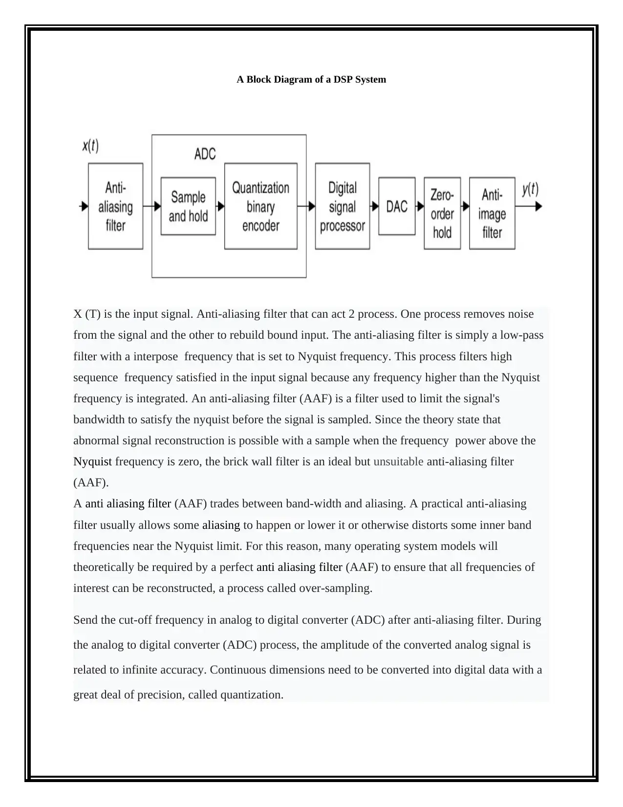
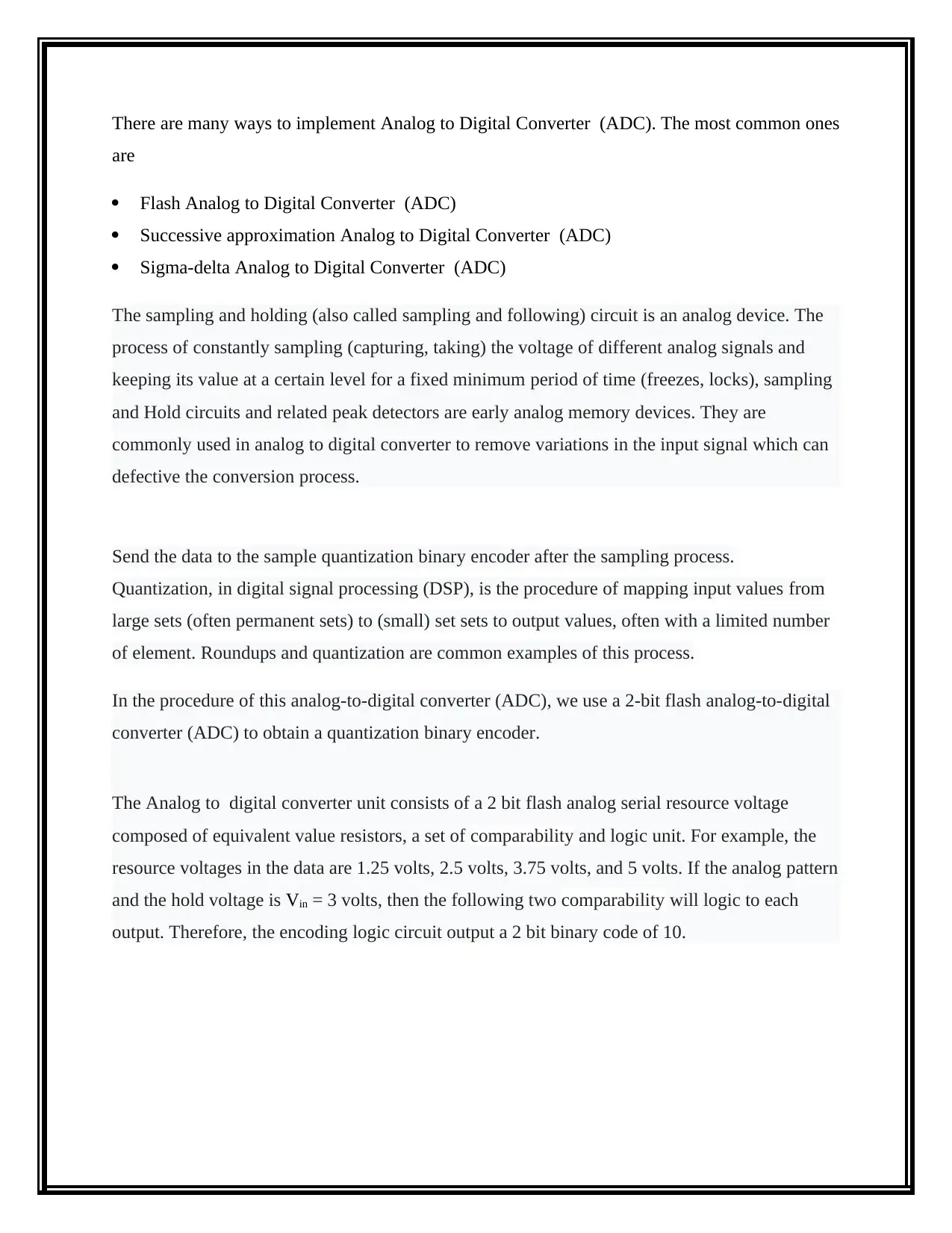
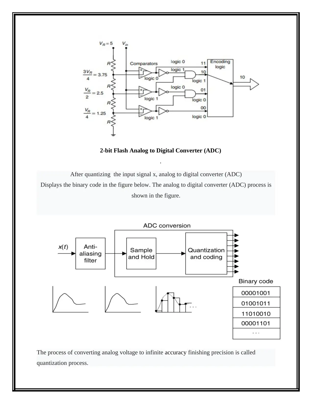
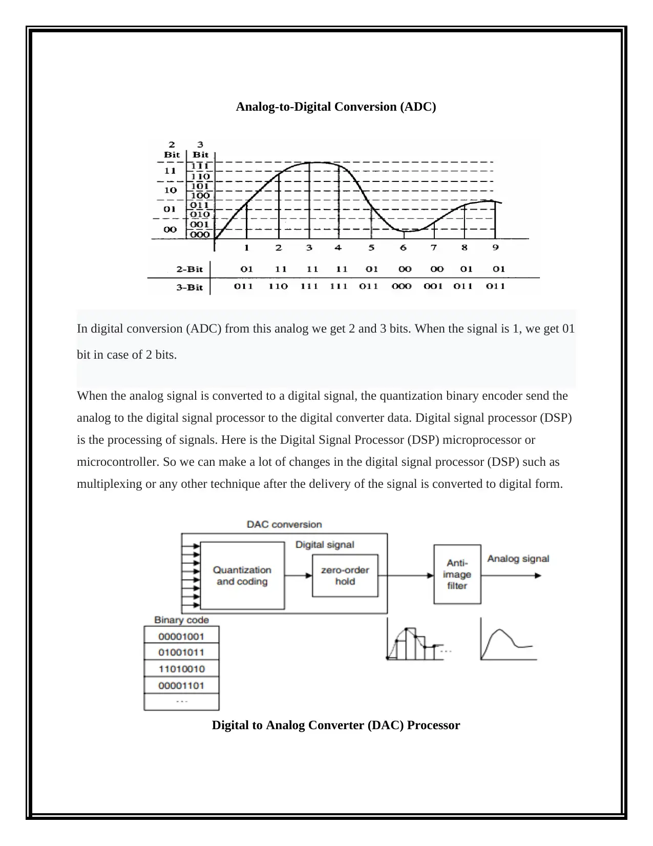
The assignment provides a detailed analysis of a Digital Signal Processing (DSP) system block diagram. It begins by explaining the role of an anti-aliasing filter in removing noise and rebuilding the input signal, highlighting its importance in satisfying the Nyquist frequency. The report then delves into the analog-to-digital conversion (ADC) process, discussing quantization techniques and the use of a 2-bit flash ADC. Following this, it describes the digital signal processor (DSP) and the digital-to-analog converter (DAC) processes, including the zero-order hold circuit and anti-image filters. The report also covers the conversion of analog to digital and digital to analog signals. The document concludes by explaining the reconstruction of the analog signal (Y(t)) after passing through the DAC and anti-image filters, providing a comprehensive overview of the DSP system's functionality and signal flow.
tabler-icon-diamond-filled.svg

Contribute Materials

Your contribution can guide someone’s learning journey. Share your documents today.
Document Page
A Block Diagram of a DSP System
X (T) is the input signal. Anti-aliasing filter that can act 2 process. One process removes noise
from the signal and the other to rebuild bound input. The anti-aliasing filter is simply a low-pass
filter with a interpose frequency that is set to Nyquist frequency. This process filters high
sequence frequency satisfied in the input signal because any frequency higher than the Nyquist
frequency is integrated. An anti-aliasing filter (AAF) is a filter used to limit the signal's
bandwidth to satisfy the nyquist before the signal is sampled. Since the theory state that
abnormal signal reconstruction is possible with a sample when the frequency power above the
Nyquist frequency is zero, the brick wall filter is an ideal but unsuitable anti-aliasing filter
(AAF).
A anti aliasing filter (AAF) trades between band-width and aliasing. A practical anti-aliasing
filter usually allows some aliasing to happen or lower it or otherwise distorts some inner band
frequencies near the Nyquist limit. For this reason, many operating system models will
theoretically be required by a perfect anti aliasing filter (AAF) to ensure that all frequencies of
interest can be reconstructed, a process called over-sampling.
Send the cut-off frequency in analog to digital converter (ADC) after anti-aliasing filter. During
the analog to digital converter (ADC) process, the amplitude of the converted analog signal is
related to infinite accuracy. Continuous dimensions need to be converted into digital data with a
great deal of precision, called quantization.
tabler-icon-diamond-filled.svg

Secure Best Marks with AI Grader

Need help grading? Try our AI Grader for instant feedback on your assignments.
Document Page
There are many ways to implement Analog to Digital Converter (ADC). The most common ones
are
Flash Analog to Digital Converter (ADC)
Successive approximation Analog to Digital Converter (ADC)
Sigma-delta Analog to Digital Converter (ADC)
The sampling and holding (also called sampling and following) circuit is an analog device. The
process of constantly sampling (capturing, taking) the voltage of different analog signals and
keeping its value at a certain level for a fixed minimum period of time (freezes, locks), sampling
and Hold circuits and related peak detectors are early analog memory devices. They are
commonly used in analog to digital converter to remove variations in the input signal which can
defective the conversion process.
Send the data to the sample quantization binary encoder after the sampling process.
Quantization, in digital signal processing (DSP), is the procedure of mapping input values from
large sets (often permanent sets) to (small) set sets to output values, often with a limited number
of element. Roundups and quantization are common examples of this process.
In the procedure of this analog-to-digital converter (ADC), we use a 2-bit flash analog-to-digital
converter (ADC) to obtain a quantization binary encoder.
The Analog to digital converter unit consists of a 2 bit flash analog serial resource voltage
composed of equivalent value resistors, a set of comparability and logic unit. For example, the
resource voltages in the data are 1.25 volts, 2.5 volts, 3.75 volts, and 5 volts. If the analog pattern
and the hold voltage is Vin = 3 volts, then the following two comparability will logic to each
output. Therefore, the encoding logic circuit output a 2 bit binary code of 10.
Document Page
2-bit Flash Analog to Digital Converter (ADC)
.
After quantizing the input signal x, analog to digital converter (ADC)
Displays the binary code in the figure below. The analog to digital converter (ADC) process is
shown in the figure.
The process of converting analog voltage to infinite accuracy finishing precision is called
quantization process.
Document Page
Analog-to-Digital Conversion (ADC)
In digital conversion (ADC) from this analog we get 2 and 3 bits. When the signal is 1, we get 01
bit in case of 2 bits.
When the analog signal is converted to a digital signal, the quantization binary encoder send the
analog to the digital signal processor to the digital converter data. Digital signal processor (DSP)
is the processing of signals. Here is the Digital Signal Processor (DSP) microprocessor or
microcontroller. So we can make a lot of changes in the digital signal processor (DSP) such as
multiplexing or any other technique after the delivery of the signal is converted to digital form.
Digital to Analog Converter (DAC) Processor
tabler-icon-diamond-filled.svg

Secure Best Marks with AI Grader

Need help grading? Try our AI Grader for instant feedback on your assignments.
Document Page
The process of converting from digital to analog to digital is shown in the figure. As shown in
the figure, the digital to analog processor (DAC) unit receives the binary code from the digital
signal processor.
This pattern is then converted to binary code using a zero order hold circuit to re-produce the
hold and signal. Suppose that spectrum distortion due to pattern and hold impact can be ignored
for our view, the recover sample and hold signal are further procedure using anti-image filters.
Finally, the analog signal is received.
Zero Order Hold (ZOH) is a mathematical model for the reconstruction of practical signals
performed by a conventional digital to analog converter (DAC). In this process, when the zero
order hold receives an analog conversion signal from digital, the zero order will have the impact
of converting the value of each sample for a sample interval into a discrete time signal.
After receiving the signal from zeroth order hold that anti image filter in a mixed-signal
system (analog and digital), a reconstruction filter, sometimes called an anti-imaging
filter, is used to construct a smooth analog signal from a digital input, as in the case of a
digital to analog converter Digital to Analog Converter (DAC) or other sampled data output
device. In this process we obtained the smooth analog signal from a digital input. Finally we
obtained the analog signal Y(t).
chevron_up_icon
1 out of 5
circle_padding
hide_on_mobile
zoom_out_icon
logo.png

Your All-in-One AI-Powered Toolkit for Academic Success.

Available 24*7 on WhatsApp / Email

[object Object]