EEE/CSE 120 Hardware Lab 4 Design Project
VerifiedAdded on 2019/09/19
|5
|1535
|470
Project
AI Summary
This document outlines the requirements for the EEE/CSE 120 Hardware Lab 4 Design Project, focusing on creating a synchronous sequential machine to announce the winner of a game called Screwball. Students are required to design two conceptually different finite-state machines, simulate them using Logisim, and then build one of the designs using TTL parts. The project involves both software simulation and hardware implementation, with specific grading criteria for each phase. The document also includes lab rules, available ICs, and deadlines for the project.
Hardware Lab 4: EEE/CSE 120 Design Project
Fall 2016
Background: The Scoring in Screwball
There is a game called Screwball. Every time a ball is put in play, either player 1 scores a point
or player 2 scores a point. A winner is declared when one player is ahead by 2 points. Starting
with a score of 0:0 for P1 vs. P2, a game might progress as follows:
0:1 1:1 2:1 3:1 (P1 Wins!)
The Application: The Win Announcer
Your task is to develop a synchronous sequential machine that uses information about which
player scores a point at each stage of a game to indicate BOTH when a player wins and which
player wins. Your design should include one reset input to initialize your WIN ANNOUNCER
(this may be a synchronous or asynchronous input as you desire). The outputs from your design
should indicate BOTH when a win has occurred and which player is the winner.
All information to complete this design may not be specified. Write down and report any
assumptions that you make in your design.
Be sure to use debounced “logic switches” for driving the clock input to the flip-flops.
Deliverables
You are to design two CONCEPTUALLY different finite-state synchronous machines. A
design which differs only by the type of flip flop used (e.g., J-K vs. D) or number of states is not
considered conceptually different.
First, you will need to implement both designs using Logisim and demonstrate to the
CSE/EEE 120 simulation TA’s in GWC 185 that both designs work correctly by the
software due date (See Table 1 below).
You may demo this by either 1) opening your file using the computer reserved by the TA on duty
or 2) asking the TA to test your circuit on your laptop. You will need to bring with you a
printout of your report template into which you’ve cut/pasted your Logisim circuits. It
makes most sense to complete the lab template and print it before you go and demonstrate the
designs to the TA. You must have your design simulation working before asking the TA to
test it because you will be given only one chance to prove that it works. You must also be
able to defend your design; the TA’s will be asking questions to make sure that your design is
your own original work. Upon completion of your simulation demonstration, the TA’s will sign
and apply a grade to your report template. You also need to include these simulations into your
lab report template.
Second, you will need to implement ONE design using the TTL parts you used in earlier lab
work and demonstrate to only a CSE/EEE 120 hardware TA that your circuit works
correctly. You must complete this demo by the due date (See Table 1 below). After reviewing
the simulation TA’s signature on your Logisim schematic printout, the hardware TA’s will test
your design and stamp the design pages of your completed report template. You must be able to
explain why your circuit responds the way it does to a given input data stream. You must have
your report template completed and bring it with you to your in-lab hardware
demonstration. Your completed report template will be collected by the hardware TA at the
Paraphrase This Document
Need a fresh take? Get an instant paraphrase of this document with our AI Paraphraser
conclusion of your demonstration.
You must use the design project template for your report.
Lab project make-ups will be allowed ONLY with written permission from your instructor.
You may discuss this project with each other; however, you must provide an individual report.
In addition:
• You must go to the GWC 185 individually to demonstrate your simulation
of both designs AND (Write up the Lab Report BEFORE you come to the hardware lab).
• You must go to the hardware lab individually to build one circuit in order
to have your individual report count.
Grading Policy
The grade will be allocated as follows:
30% Design Simulation With Logisim
• 15% for the design of the first circuit and demonstration.
• 15% for the design of the second circuit and demonstration.
•
7
0
%
B
u
i
l
d
O
n
e
D
e
s
i
g
n
i
n
t
h
e
H
a
r
d
w
a
r
e
L
a
b
a
n
d
L
a
b
R
e
p
o
r
t
• 30% demonstration of one design in the hardware lab.
• 11% for documentation in the report of how the first circuit performs the
application.
• 11% for documentation in the report of how the second circuit performs
the application.
• 5% for establishing reasonable criteria for picking one design as the “best”
design. (The one design you build in the hardware lab does not need to be the “best”
design.)
• 8% for picking a preferred, “best” design.
• 5% for following template guidelines.
5% (Extra Credit) Completed SelfAssessment Worksheet
5% (Extra Credit) for signing up for a Hardware Demonstration time slot on a Monday,
Tuesday or Wednesday. 10% extra credit for signing up for the SW Demonstration time on
the first 2 days of the week (You must perform it on that day to get the extra credit)
Table 1: Period of Performance
Instructor
Begin Simulation Demo
Complete Simulation Demo
Begin Hardware Demo
Complete Hardware Demo
Reisslein & Hartin & Goryll
NOV 15
NOV 18
r
d
w
a
r
e
L
a
b
a
n
d
L
a
b
R
e
p
o
r
t
• 30% demonstration of one design in the hardware lab.
• 11% for documentation in the report of how the first circuit performs the
application.
• 11% for documentation in the report of how the second circuit performs
the application.
• 5% for establishing reasonable criteria for picking one design as the “best”
design. (The one design you build in the hardware lab does not need to be the “best”
design.)
• 8% for picking a preferred, “best” design.
• 5% for following template guidelines.
5% (Extra Credit) Completed SelfAssessment Worksheet
5% (Extra Credit) for signing up for a Hardware Demonstration time slot on a Monday,
Tuesday or Wednesday. 10% extra credit for signing up for the SW Demonstration time on
the first 2 days of the week (You must perform it on that day to get the extra credit)
Table 1: Period of Performance
Instructor
Begin Simulation Demo
Complete Simulation Demo
Begin Hardware Demo
Complete Hardware Demo
Reisslein & Hartin & Goryll
NOV 15
NOV 18
⊘ This is a preview!⊘
Do you want full access?
Subscribe today to unlock all pages.
Trusted by 1+ million students worldwide
NOV 28
DEC 02
Chickamenahalli and Matar
NOV 7th
NOV 10th
NOV 14th
NOV 18th
LAB MANAGER’S RULES FOR PERFORMANCE
• You will only be allowed to do the project during the assigned times. If
you miss the calendar dates, you will not be allowed to do the lab project unless you have
a WRITTEN NOTE signed by your course professor.
• Hardware Demo: You must have your lab report completed before you start
the lab demo since you will need to give it to the lab TA at the completion of the demo.
(Having your report finished will help you complete the lab project in the allotted time.) You
will not be allowed to do any practice runs of the lab project inside of GWC-273. You
must be ready to complete the entire lab project when you come into GWC-273. However,
outside of GWC-273 you may consult with anyone you wish to obtain help in designing the
lab project.
• Hardware Demo: You will have ONLY 2 HOURS to complete the lab
project in GWC273. You must work alone with no lab partners to assist you. No friends,
relatives or tutors may be with you. You may bring any textbooks, notes, reference
books, lab notes, lab experiments, and lab reports into the GWC-273 lab area. You will
definitely need your PIN-OUT diagrams of the IC chips. You will not be allowed to take
any breaks from your 2-hour shift except for restroom and water. (Sorry: but you cannot
bring in your own breadboards and IC chips because that would give you an unfair
advantage over other students in the GWC-273 lab.)
• Notice: Make sure you do the project ONLY during the hours in which any
EEE/CSE 120 Hardware Lab TA is on duty inside of GWC-273. Only these TAs can assist,
monitor and check-off your project. TAs in other courses are not permitted to assist you do the
lab project.
• You will be able to use any of the IC’s we have in the lab for completing
your project. Check in the lab if you are not sure which IC’s are available. Be aware that
in GWC 273 we DO NOT have the following IC’s available: 7421, 7430, 74133, 74174,
74375.
• Hardware Lab TA’s on duty will assist you ONLY if there is broken lab
equipment. Hardware Lab TA’s will NOT assist you with troubleshooting or debugging
your project lab design circuit.
Notice: If you are thinking of omitting this lab project from your schedule, be reminded that
parts of this lab project may show up on the final exam for this course!
You can only design your circuit with the ICs that are available in GWC 273
Paraphrase This Document
Need a fresh take? Get an instant paraphrase of this document with our AI Paraphraser
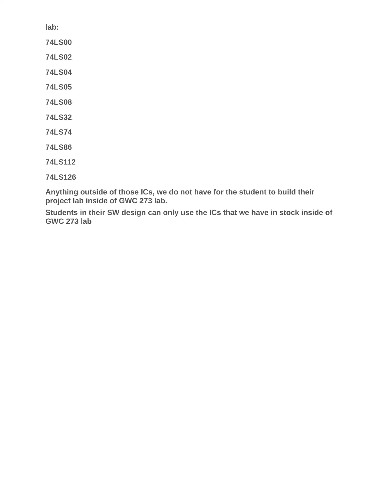
lab:
74LS00
74LS02
74LS04
74LS05
74LS08
74LS32
74LS74
74LS86
74LS112
74LS126
Anything outside of those ICs, we do not have for the student to build their
project lab inside of GWC 273 lab.
Students in their SW design can only use the ICs that we have in stock inside of
GWC 273 lab
74LS00
74LS02
74LS04
74LS05
74LS08
74LS32
74LS74
74LS86
74LS112
74LS126
Anything outside of those ICs, we do not have for the student to build their
project lab inside of GWC 273 lab.
Students in their SW design can only use the ICs that we have in stock inside of
GWC 273 lab
1 out of 5
Related Documents

Your All-in-One AI-Powered Toolkit for Academic Success.
+13062052269
info@desklib.com
Available 24*7 on WhatsApp / Email
![[object Object]](/_next/static/media/star-bottom.7253800d.svg)
Unlock your academic potential
Copyright © 2020–2026 A2Z Services. All Rights Reserved. Developed and managed by ZUCOL.