Electrical Circuit Design Homework - Semester 2, University XYZ

Verified

Added on  2023/06/10

|15
|1471
|226
Homework Assignment
AI Summary
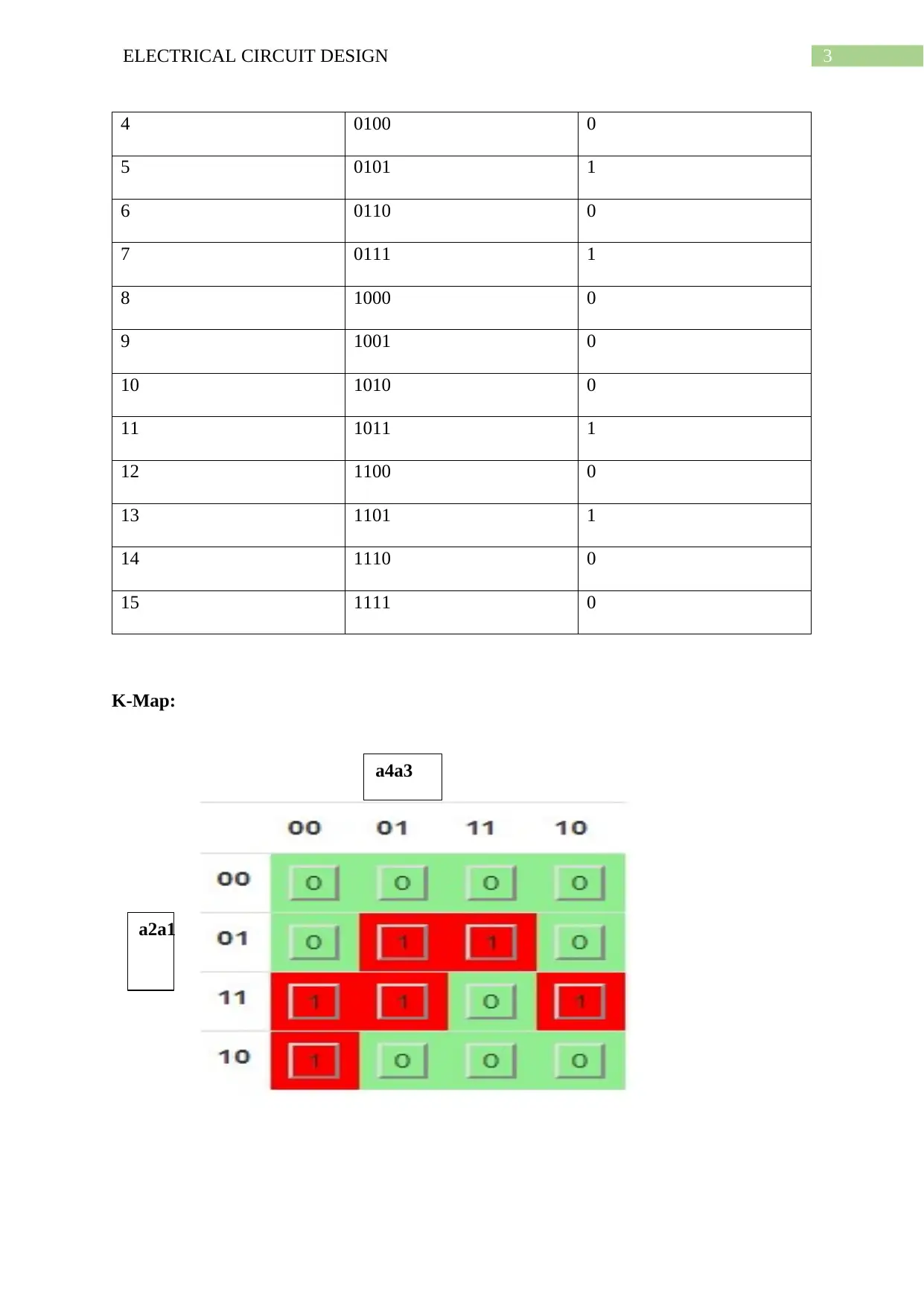
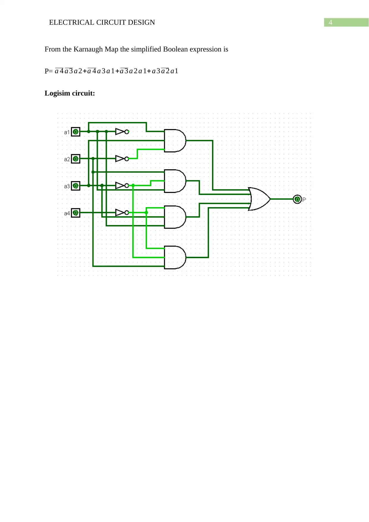
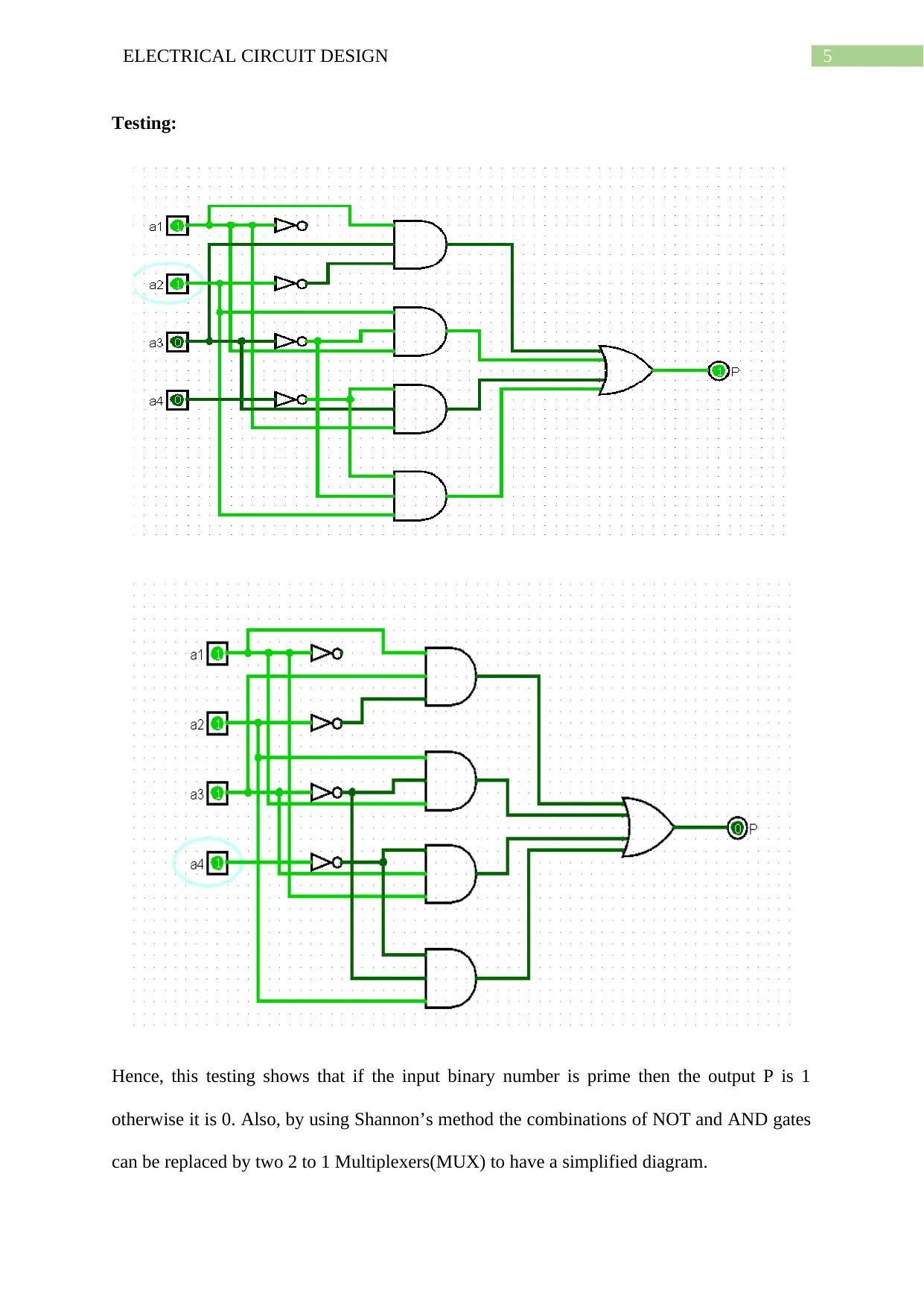
This document presents a comprehensive solution to an electrical circuit design assignment. The solution begins with an analysis of a traffic light system, detailing state transitions and outputs. It then moves on to designing a combinational circuit for prime number detection using a 4-bit binary number, including a truth table, K-map simplification, and a Logisim circuit implementation. The assignment further explores state transition diagrams, state tables, and K-maps to derive state equations for a sequential circuit. It then proceeds to design circuits using 2 to 4 decoders. Finally, the solution includes Verilog code for a 4-bit full adder module and an 8-bit full adder, demonstrating behavioral code and modular design principles.
Document Page
Running head: ELECTRICAL CIRCUIT DESIGN
ELECTRICAL CIRCUIT DESIGN
Name of the Student
Name of the University
Author Note
tabler-icon-diamond-filled.svg

Paraphrase This Document

Need a fresh take? Get an instant paraphrase of this document with our AI Paraphraser
Document Page
1ELECTRICAL CIRCUIT DESIGN
Response to question 1:
s
As the arrow moves right to left it gets shorter in length. Hence, the 25 traffic lights from A
to Y will also behave accordingly. In the bottom figure 4 states are shown in total as the
arrow becomes shorter and in the last state all the lights are off i.e. the arrow is not displayed.
State Lights On
State 1 11 (A,D,J,Q,W,K,L,M,N,O,P)
State 2 9(B,F,L,S,X,M,N,O,P)
State 3 7(C,H,N,U,Y,O,P)
State 4 0
Hence, the transition between states occur according to number of lights on/off and based on
which lights are on/off. The state output is 1 when the arrow is displayed, otherwise it is 0. In
the first three states the state output is 1 and in the last state it is 0. The state inputs are
considered as number of lights that are on in that state.
Document Page
2ELECTRICAL CIRCUIT DESIGN
State diagram:
Response to question 2:
A number is a prime number if it is exactly divisible by 1 and that number itself. Now, a
combinational circuit has been designed to detect a 4-bit binary number is prime or not.
The four-bit number is A = a4 a3 a2 a1.
Here, the MSB of the number is a1 and LSB is a4. The truth table gives the prime number for
which the output is 1.
Decimal equivalent Binary (a4 a3 a2 a1) Output (True=1, False=0)
0 0000 0
1 0001 0
2 0010 1
3 0011 1
State 4
State 1
State 3
State 2
9/1
7/1
0/0
11/1
Document Page
3ELECTRICAL CIRCUIT DESIGN
4 0100 0
5 0101 1
6 0110 0
7 0111 1
8 1000 0
9 1001 0
10 1010 0
11 1011 1
12 1100 0
13 1101 1
14 1110 0
15 1111 0
K-Map:
a4a3
a2a1
tabler-icon-diamond-filled.svg

Paraphrase This Document

Need a fresh take? Get an instant paraphrase of this document with our AI Paraphraser
Document Page
4ELECTRICAL CIRCUIT DESIGN
From the Karnaugh Map the simplified Boolean expression is
P= a 4 a 3 a 2+a 4 a 3 a 1+a 3 a 2 a 1+ a 3 a 2 a1
Logisim circuit:
Document Page
5ELECTRICAL CIRCUIT DESIGN
Testing:
Hence, this testing shows that if the input binary number is prime then the output P is 1
otherwise it is 0. Also, by using Shannon’s method the combinations of NOT and AND gates
can be replaced by two 2 to 1 Multiplexers(MUX) to have a simplified diagram.
Document Page
6ELECTRICAL CIRCUIT DESIGN
Response to question 3:
State transition diagram:
According to the diagram the state table is constructed in the following rule. The four circles
represent 4 states of the machine. From one state to another state transitions occur based on
the input given which is specified beside the arrows before the slash. After the slash the
output of the system is specified. A loop indicates there is no state change i.e. the machine
remains in the same state irrespective of the input.
It is considered that the states of the system are Q1 and Q2. The input and output of the
system are x and Z respectively. Moreover, D filp-flop is considered for the circuit
implementation. Hence, D1, D2 and Z are the outputs in the logic expression.
tabler-icon-diamond-filled.svg

Paraphrase This Document

Need a fresh take? Get an instant paraphrase of this document with our AI Paraphraser
Document Page
7ELECTRICAL CIRCUIT DESIGN
State table:
Present State Next State Output
Q1Q2
00
01
10
11
x=0 x=1 x=0 x=1
00 01 0 0
10 11 0 0
00 01 0 0
10 11 1 1
Now, from the state table the state equations are found by K-maps.
K-map for Z:
00 01 11 10
0 0 0 1 0
1 0 0 1 0
Hence, simplified SOP of Z = Q1Q2
Q1Q2
x
Document Page
8ELECTRICAL CIRCUIT DESIGN
K-map for D1:
00 01 11 10
0 0 1 1 0
1 0 1 1 0
Hence, simplified SOP of D1 = Q2
K-Map for D2:
00 01 11 10
0 0 0 0 0
1 1 1 1 1
Hence, simplified SOP of D2 = x.
Therefore, the state equations are
Z = Q1Q2
D1 = Q2
D2 = x
Q1Q2
x
Q1Q2
x
Document Page
9ELECTRICAL CIRCUIT DESIGN
Schematic diagram:
Response to question 4:
tabler-icon-diamond-filled.svg

Paraphrase This Document

Need a fresh take? Get an instant paraphrase of this document with our AI Paraphraser
Document Page
10ELECTRICAL CIRCUIT DESIGN
From the above circuit the logic expressions of X and Y are
X= (A ⊕ B) ⊕ C = (AB’ + BA’)
Y = AC + BC + AB
2 to 4 decoder circuit:
Implementation of X:
Document Page
11ELECTRICAL CIRCUIT DESIGN
Implementation of Y:
Response to question 5:
The Verilog behavioural code for the four bit-full adder module having three inputs a, b, cin
and two outputs sum and cout respectively is given below.
Verilog code:
module fulladder_4bit ( a ,b ,sum ,cout );
output [3:0] sum ;
output cout ;
input [3:0] a ;
input [3:0] b ;
wire [2:0]s;
full_adder u0 (a[0],b[0],1'b0,sum[0],s[0]);
full_adder u1 (a[1],b[1],s[0],sum[1],s[1]);
chevron_up_icon
1 out of 15
circle_padding
hide_on_mobile
zoom_out_icon
[object Object]