Electrical and Electronic Fundamentals: Circuit Analysis and Devices
VerifiedAdded on 2020/11/23
|19
|2814
|203
Homework Assignment
AI Summary
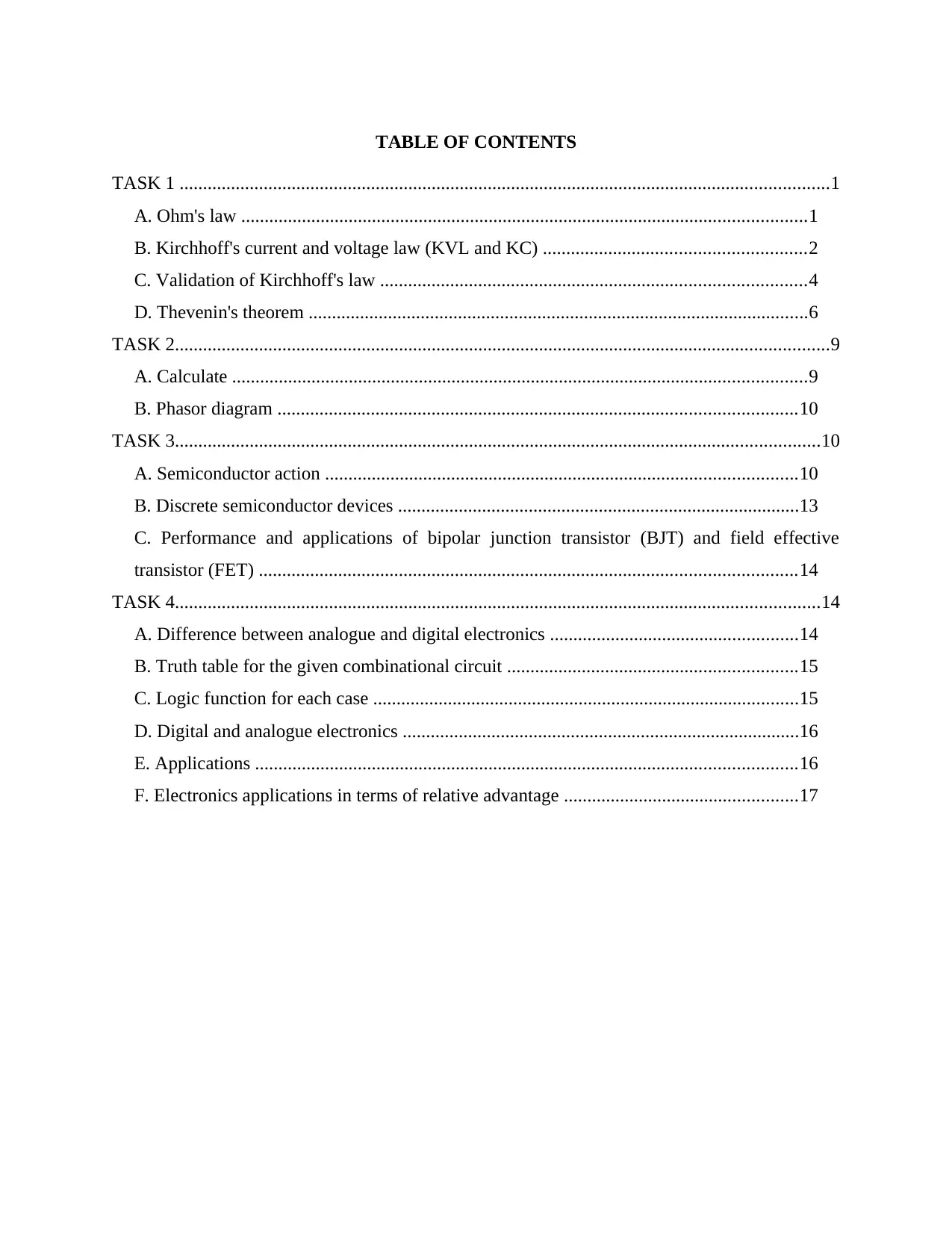
This assignment solution covers fundamental concepts in electrical and electronic engineering. It begins with Ohm's law and Kirchhoff's laws, including validation through circuit simulation and breadboard implementation. Thevenin's theorem is explained and applied to circuit simplification. The assignment then delves into AC circuit analysis, including calculations for inductive and capacitive reactance, impedance, and phase angles. Semiconductor action is discussed, focusing on diodes, Zener diodes, and transistors as switches. Discrete semiconductor devices and the performance and applications of bipolar junction transistors (BJTs) and field-effect transistors (FETs) are also examined. Finally, the assignment contrasts analog and digital electronics, analyzes a combinational circuit, and explores electronic applications.

ELECTRICAL AND
ELECTRONIC
FUNDAMENTAL
ELECTRONIC
FUNDAMENTAL
Paraphrase This Document
Need a fresh take? Get an instant paraphrase of this document with our AI Paraphraser

TABLE OF CONTENTS
TASK 1 ...........................................................................................................................................1
A. Ohm's law .........................................................................................................................1
B. Kirchhoff's current and voltage law (KVL and KC) ........................................................2
C. Validation of Kirchhoff's law ...........................................................................................4
D. Thevenin's theorem ...........................................................................................................6
TASK 2............................................................................................................................................9
A. Calculate ...........................................................................................................................9
B. Phasor diagram ...............................................................................................................10
TASK 3..........................................................................................................................................10
A. Semiconductor action .....................................................................................................10
B. Discrete semiconductor devices ......................................................................................13
C. Performance and applications of bipolar junction transistor (BJT) and field effective
transistor (FET) ...................................................................................................................14
TASK 4..........................................................................................................................................14
A. Difference between analogue and digital electronics .....................................................14
B. Truth table for the given combinational circuit ..............................................................15
C. Logic function for each case ...........................................................................................15
D. Digital and analogue electronics .....................................................................................16
E. Applications ....................................................................................................................16
F. Electronics applications in terms of relative advantage ..................................................17

TASK 1
A. Ohm's law
According to the Ohm's law the current (I) flowing through a conductor is directly
proportional to voltage drop (V) through it at constant temperature. The proportionality constant
is defined as the resistance. Thus, the expression of Ohm's law is given by:
V I∝
V/I = R
Where R is constant of proportionality and is known as Resistance.
For different readings of voltage (Volt) and current (Ampere) the when graph is plotted then a
straight line is obtained. The V is plotted on y axis while I is plotted on x axis of the graph. The
slope or gradient of the curve is known as Resistance (R) and its dimensional unit is ohm.
I (Ampere) V (Volt)
0.21 2
0.38 4
0.57 6
0.84 8
0.99 10
1
Illustration 1: Circuit diagram
⊘ This is a preview!⊘
Do you want full access?
Subscribe today to unlock all pages.

Trusted by 1+ million students worldwide

The slope R = V/I. In the figure highlighted slope = 7V / 0.7A = 10 Ohm
Thus, between two points the slope can be calculated as : ΔV / ΔI
Where ΔV is the potential difference between two points and ΔI is the current flowing between
two points. Thus, the slope at point V = 2V and I=0.2A is given by the gradient expression:
R= (2-0) / (0.2-0) = 10 Ohm = Slope of the curve
B. Kirchhoff's current and voltage law (KVL and KC)
KVL:
As per this law, the sum of potential differences in a closed loop must be equal to zero.
2
Illustration 2: V-I plot for calculating slope
Paraphrase This Document
Need a fresh take? Get an instant paraphrase of this document with our AI Paraphraser

For example in the circuit given above both 1 and 2 are closed loops. When clockwise path is
followed in loop 1 then we get:
V1 + V2 – Vs = 0
This equation followed when passive sign convention is used.
KCL: This law analyses the current entering and leaving any particular node. The total value of
current at any node is zero.
From the circuit it can be analysed that: I1 – I2 – I3 = 0
The current which enters the node have opposite sign than the currents which are leaving the
node.
Circuit analysis:
3

The KVL and KCL can be used to analyse the circuit shown above:
On applying KVL in both closed loops ABDA and BCDB following equations are obtained.
ABDA: V1 +V2 – VS = 0
BCDB: V2 + V4 -V3 = 0
The resistance R2 and R4 are connected in series thus the currents I2 and I4 are equal. Thus,
KCL can be applied at node B only:
I1 - I2 -I3 = 0
These equations can be used to analyse the various node current and voltages.
C. Validation of Kirchhoff's law
In order to validate the Kirchhoff's law the above discussed circuit can be simulated and
then verified by using constructing circuit on breadboard and then measuring its values.
The value so resistors is measured by using multimeters and is obtained as:
R1 = 6.75 KΩ
R2 = 2.193 KΩ
R3 = 9.85 KΩ
R4 = 0.994 KΩ
4
⊘ This is a preview!⊘
Do you want full access?
Subscribe today to unlock all pages.

Trusted by 1+ million students worldwide

By KCL:
1166.3 – 196.11 – 970.11 = 0
(All values of current are measured in micro ampere). In order to find the voltage across each
resistor Ohm's law can be applied to the resistors. Similarly, by KVL in closed loops it is
observed that :
7.87 + 2.12 – 10 = 0.002
1.93 + 0.195 – 2.12 = 0.000
Thus, from this simulation Kirchhaff's law are verified.
The verification can also be performed by measuring the values of components on breadboard
implementation. 10V Supply is used on board and following values of components are measured.
V1 V2 V3 V4 I1 I2 = I4 I3
7.37 V 1.80 V 2.62 V 0.87 V 1.08 mA 0.81mA 0.25 mA
5
Paraphrase This Document
Need a fresh take? Get an instant paraphrase of this document with our AI Paraphraser

On putting these measured values in the above analysed equations of KVL and KCL following
equation is obtained:
7.37 + 1.80 – 10 = -0.82 (Loop 1)
1.80 + 0.87 – 2.62= 0.05 (Loop 2)
KCL : 1.06 – 0.81 – 0.25
Thus, from the above approaches the Kirchhaff law can be validated.
D. Thevenin's theorem
This theorem states that any linear network can be replaced with its equivalent circuit
consisting of voltage source and single resistance. The theorem is greatly useful to simplify and
analyse the complex circuits by converting them into a simple one. In order to find the Thevenin
equivalent circuit following steps must be followed:
Load resistor is removed and from open circuit voltage is calculated which is called
Thevenin voltage Vth.
To determine the equivalent Thevenin resistance (Rth) all voltage sources are shorted and
current sources are opened.
Equivalent Thevenin circuit can constructed by connecting Vth and Rth in series. The
load resistance RL is connected across open terminals of this equivalent circuit to so that
voltage, current and power can be calculated across it.
6

The load resistance is 40 thus it is removed and other voltage sources are short so that Rth can be
calculated.
Rth = (R1*R2) / (R1 + R2)
R1 = 20 Ω and R2= 10Ω so
Rth = 6.67 Ω
The Vth can be calculated as :
I = V/R = (20-10)/(20 +10) = 0.33A
Vth = V across 20 Ω resistor
= 20 – (20*0.33) = 13.33 Volt
7
calculated.
Rth = (R1*R2) / (R1 + R2)
R1 = 20 Ω and R2= 10Ω so
Rth = 6.67 Ω
The Vth can be calculated as :
I = V/R = (20-10)/(20 +10) = 0.33A
Vth = V across 20 Ω resistor
= 20 – (20*0.33) = 13.33 Volt
7
⊘ This is a preview!⊘
Do you want full access?
Subscribe today to unlock all pages.

Trusted by 1+ million students worldwide

The Thevenin equivalent circuit is given as:
Current through the circuit = I= (13.33)/ (6.67+40)
= 0.29 A
Thus, for the analysis of circuits which have variable load this theorem is helpful for the
simplification purpose.
TASK 2
A. Calculate
L = 80 mH = 0.08 H
R = 200 Ω
C = 22 uF
Source current (Is) = 40 mA = 0.04 A
8
Current through the circuit = I= (13.33)/ (6.67+40)
= 0.29 A
Thus, for the analysis of circuits which have variable load this theorem is helpful for the
simplification purpose.
TASK 2
A. Calculate
L = 80 mH = 0.08 H
R = 200 Ω
C = 22 uF
Source current (Is) = 40 mA = 0.04 A
8
Paraphrase This Document
Need a fresh take? Get an instant paraphrase of this document with our AI Paraphraser

Frequency = 50Hz
Solution:
Inductive reactance (XL) = 2пfL = 2п * 50 * 0.08 = 25.12 Ω
Capacitive reactance (XC) = 1/ (2пfC) = 1 / (2п * 50 * 22* 10^(-6)) = 144.75 Ω
Voltage across resistor (Vr) = Is * R = 0.04 * 200
= 8 V
Voltage across capacitor (VC) = Is * XC = 0.04 * 144.75
= 5.79 V
Voltage across inductor (VL) = Is * XL = 0.04 * 25.12
= 1.004 V
Impedance (Z) = [(R^2) + (XL – XC)^2]½
= [(200^2) + (25.12 – 144.75)^2]½
= 233.04 Ω
Supply voltage (Vs)= Is * Z = 0.04 * 233.04
= 9.32 Volt
Current flowing through the circuit = Vs/Z = 9.32 / 233.04
= 39.9 mA
Phase angle (ф)
Cos ф = R /Z = 200 / 233.04
Cos ф = 0.858
ф = 30.9 degree (Lagging)
9

B. Phasor diagram
TASK 3
A. Semiconductor action
The semiconductor actions can be demonstrated by evaluating the working principle of
following devices.
Diode:
A diode is a semiconductor device which conducts in one direction only. Thus, when the
polarity of biasing is reversed its current flow characteristics are also changed. The
semiconductor diode consist of p type and n type semiconductors which forms a junction called
p-n junction. P type semiconductor are formed by doping trivalent impurities like Al, Ga are
used while for making n type semiconductor pentavalent impurities such as phosphorus and As
are used. When p-n diode is forward biased then holes from p side and electrons from n side are
moved towards junction and thus a depletion layer is formed. This depletion layer prevents the
10
⊘ This is a preview!⊘
Do you want full access?
Subscribe today to unlock all pages.

Trusted by 1+ million students worldwide
1 out of 19
Related Documents

Your All-in-One AI-Powered Toolkit for Academic Success.
+13062052269
info@desklib.com
Available 24*7 on WhatsApp / Email
Unlock your academic potential
Copyright © 2020–2025 A2Z Services. All Rights Reserved. Developed and managed by ZUCOL.