Electrical Engineering Assignment: Op-Amps and Logic
VerifiedAdded on 2022/09/05
|10
|1933
|19
Homework Assignment
AI Summary
This electrical engineering assignment solution covers several key topics in the field. Task 1 differentiates between analogue and digital quantities, signals, sensors, and actuators, explaining their functions and providing examples of interface circuitry. Task 2 analyzes an inverting operational amplifier circuit, calculating the feedback resistor value for a gain of 1000 and verifying the gain using Multisim software. It also discusses the frequency response and characteristics of an ideal op-amp. Task 3 examines a differential amplifier circuit, detailing its truth table, function, and operation, with simulation results. Finally, Task 4 simplifies a Boolean expression using Karnaugh maps, minimizes the resulting circuit, and provides a truth table to prove the minimized circuit's functionality, concluding with the implemented circuit using NAND gates and its simulation.
Task 1
An analogue quantities are those quantities whose magnitudes or values varies continously for
example room temperature. Digital quantities on the other hand, have a discrete set of values for
instance, digital clock
An analogue signal is an electrical waveform representing physical measurements, its amplitude
varies continously. The analoque signal signal is uniquely defined for all time values. The period
of analog signal is dependent on the frequency of the source. A digital signal on the other hand
uses discrete set of values to reprsent information. Analoq quantity consumes less bandwidth as
compared to the digital quantity.
Sensors- are modules or devices that detects a change in events or its environment and responds
to the changes by sending a signal to other electronic machines usually a processor.
Actuator- is a device that utilizes a control signal to control and move a system or mechanism.
Interface circuitry- are responsible for connecting electronics circuits such as logic gates to the
outside world.
An example of analog input that is used to control analog output is a mechanical switch or
sensors or light dependent resistors. The switch is used to control analog output which in our
case could be an LED or actuators. Input interface circuitry connects logic gates and other
electronic circuits to other devices or rather outside world. Electronics circuits process signals
from sensors or switches so as to control LED or actuators(ElectronicsTutorial, n.d). Sensors
provides information about physical quantities such as temperature, lighting and pressure. Light
dependent resistors are normally used to switch on and off LEDS. The LEDS are switched OFF
when there high light intensity and ON when light intensity is at its lowest levels
Task 2
Part A
Paraphrase This Document
Need a fresh take? Get an instant paraphrase of this document with our AI Paraphraser
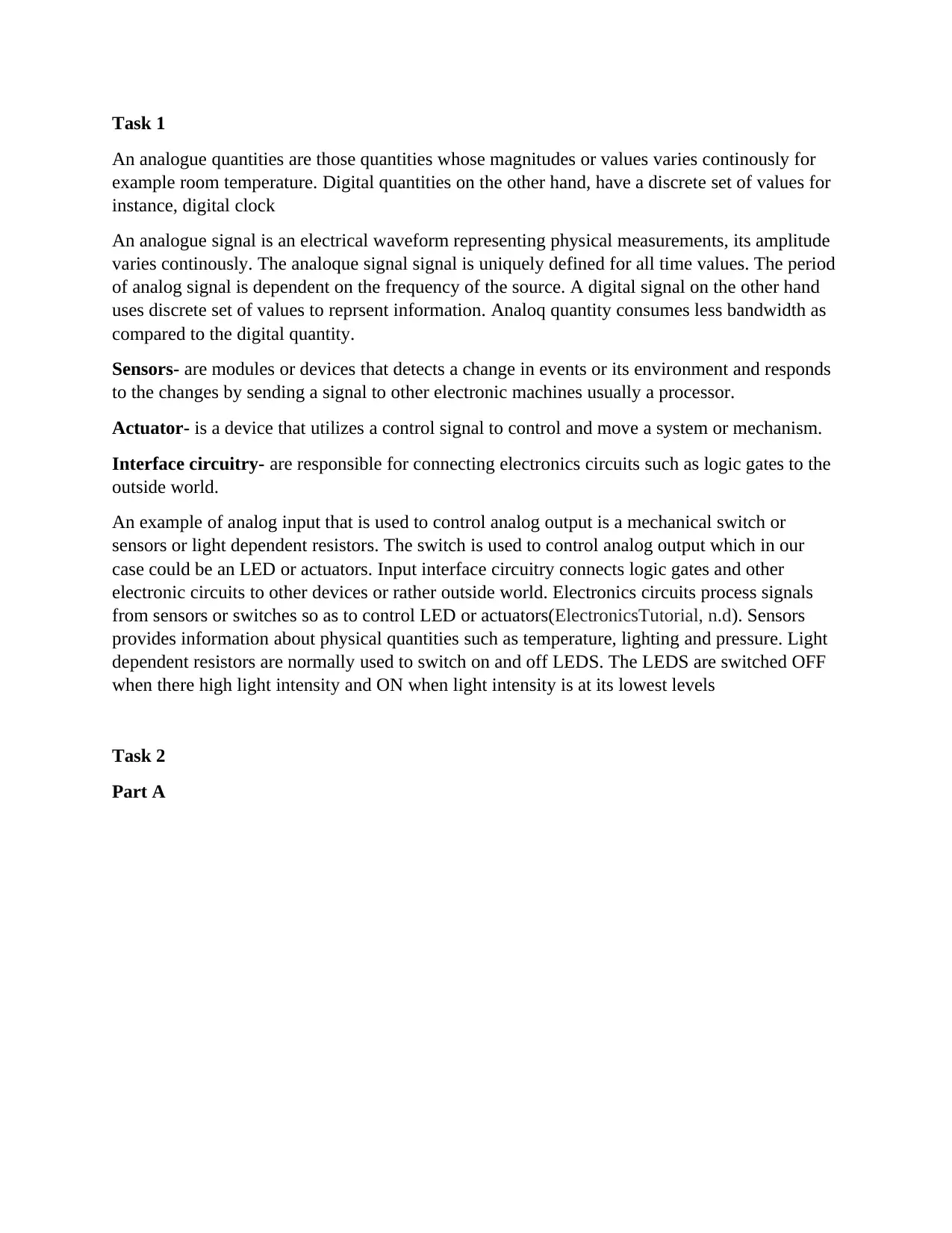
figure 2.1: Inverting operational amplifier circuit.
a) Value of feedback resistor that can achieve a voltage gain of 1000
Gain, Av of an inverting operational amplifier is given by the formula below
Gain = output voltage
input voltage = −Rf
Rin ( Bird , 2017)……………1
Given, Gain = 1000, Rin = 100 Ω
From equation 1, feedback resistor value is computed as shown below
Rf = Gain * Rin
= 1000 * 100
= 100kΩ
To proof that the gain of 1000 has been achieved, the circuit of figure 1 was implemented
on Multisim software. The input and output voltages magnitudes as displayed on the
virtual oscilloscope are as shown in figure 2.2.
Channel A is the input signal and the magnitude is
Vp-p = 2mV/ division * 5 divisions
= 10 mV
Channel B of the oscilloscope represent the output signal and the magnitude is
Vp-p = 5V/ division * 2 divisions
= 10 V
From formula 1
Gain = output voltage
input voltage = 10
0.01
= 1000
Thus, the gain of 1000 was achieved.
Figure 2.2: Input and output voltages of the op-amp
b) Gain of the circuit of figure 2.1 is constant at 60dB (20log (Av =1000)) from zero hertz to
a certain frequency known as cut-off frequency. The gain then falls by 3dB from the
initial or maximum value. The significance of the 3dB drop of the gain from the initial
value is to enable us determine the cut-off frequency of the circuit.
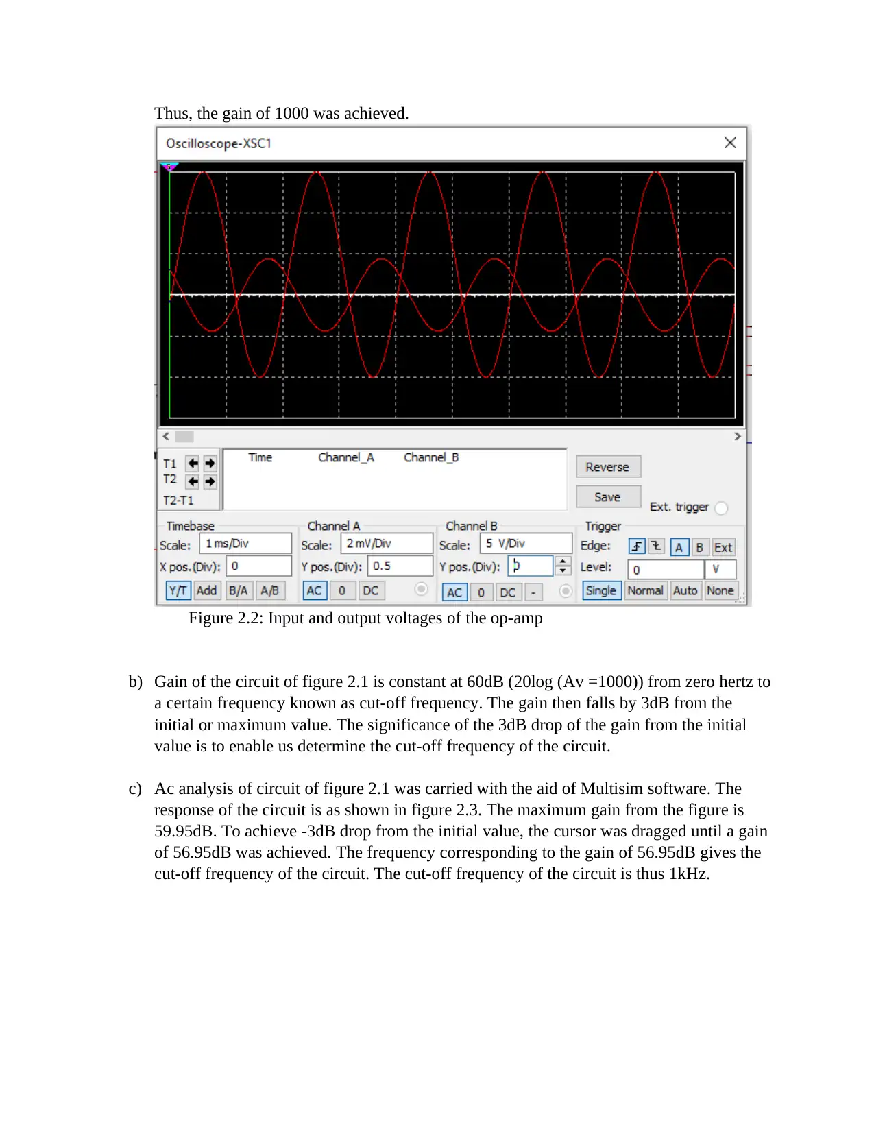
c) Ac analysis of circuit of figure 2.1 was carried with the aid of Multisim software. The
response of the circuit is as shown in figure 2.3. The maximum gain from the figure is
59.95dB. To achieve -3dB drop from the initial value, the cursor was dragged until a gain
of 56.95dB was achieved. The frequency corresponding to the gain of 56.95dB gives the
cut-off frequency of the circuit. The cut-off frequency of the circuit is thus 1kHz.
Figure 2.2: Input and output voltages of the op-amp
b) Gain of the circuit of figure 2.1 is constant at 60dB (20log (Av =1000)) from zero hertz to
a certain frequency known as cut-off frequency. The gain then falls by 3dB from the
initial or maximum value. The significance of the 3dB drop of the gain from the initial
value is to enable us determine the cut-off frequency of the circuit.
c) Ac analysis of circuit of figure 2.1 was carried with the aid of Multisim software. The
response of the circuit is as shown in figure 2.3. The maximum gain from the figure is
59.95dB. To achieve -3dB drop from the initial value, the cursor was dragged until a gain
of 56.95dB was achieved. The frequency corresponding to the gain of 56.95dB gives the
cut-off frequency of the circuit. The cut-off frequency of the circuit is thus 1kHz.
⊘ This is a preview!⊘
Do you want full access?
Subscribe today to unlock all pages.
Trusted by 1+ million students worldwide
Figure 2.3: Frequency response of the circuit.
Part B.
Characteristics of ideal operational amplifier (Hughes, Hiley, Brown, and Mckenzie,
2012)
It has infinite power supply rejection ration and common mode rejection ratio.
It has no noise.
It has zero output impedance.
It has infinite slew rate.
It has no offset voltage.
It has infinite open loop gain.
It has infinite range of voltage at its output.
It draws no current at the input since the input impedance is infinite.
Task 3
a) Truth table for the circuit
Input A Input B Output Q
0 0 0
0 1 1
1 0 1
1 1 0
b) The function of the circuit
The circuit computes the difference between the two input voltages (inputs A and B)
Paraphrase This Document
Need a fresh take? Get an instant paraphrase of this document with our AI Paraphraser
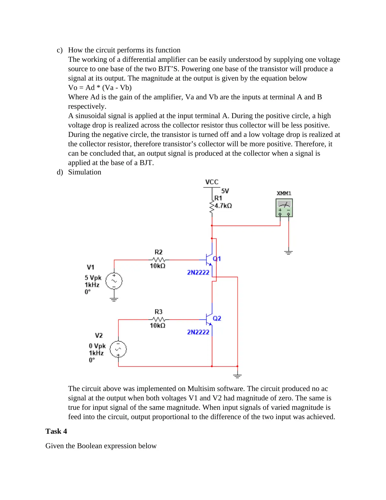
c) How the circuit performs its function
The working of a differential amplifier can be easily understood by supplying one voltage
source to one base of the two BJT’S. Powering one base of the transistor will produce a
signal at its output. The magnitude at the output is given by the equation below
Vo = Ad * (Va - Vb)
Where Ad is the gain of the amplifier, Va and Vb are the inputs at terminal A and B
respectively.
A sinusoidal signal is applied at the input terminal A. During the positive circle, a high
voltage drop is realized across the collector resistor thus collector will be less positive.
During the negative circle, the transistor is turned off and a low voltage drop is realized at
the collector resistor, therefore transistor’s collector will be more positive. Therefore, it
can be concluded that, an output signal is produced at the collector when a signal is
applied at the base of a BJT.
d) Simulation
The circuit above was implemented on Multisim software. The circuit produced no ac
signal at the output when both voltages V1 and V2 had magnitude of zero. The same is
true for input signal of the same magnitude. When input signals of varied magnitude is
feed into the circuit, output proportional to the difference of the two input was achieved.
Task 4
Given the Boolean expression below
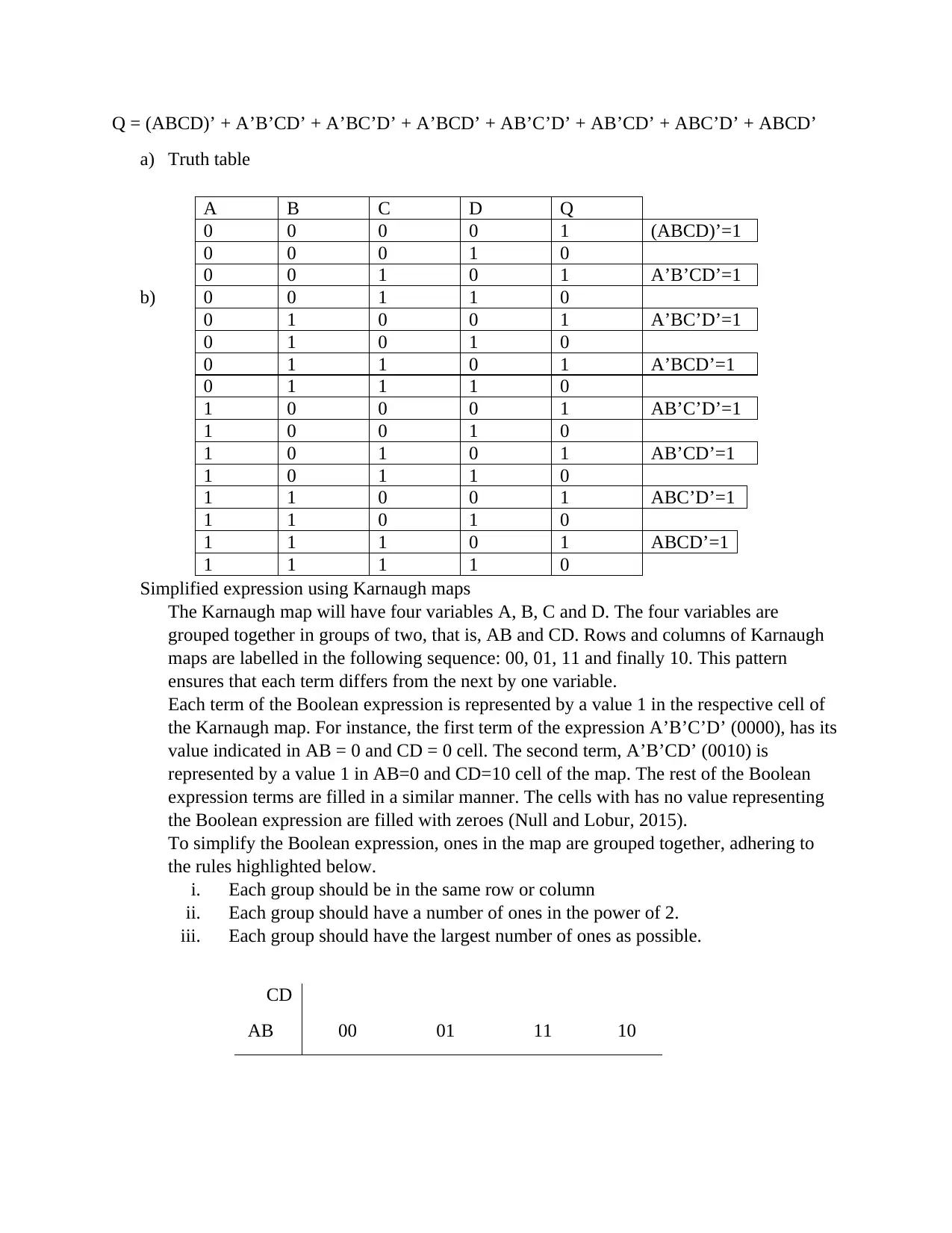
Q = (ABCD)’ + A’B’CD’ + A’BC’D’ + A’BCD’ + AB’C’D’ + AB’CD’ + ABC’D’ + ABCD’
a) Truth table
b)
Simplified expression using Karnaugh maps
The Karnaugh map will have four variables A, B, C and D. The four variables are
grouped together in groups of two, that is, AB and CD. Rows and columns of Karnaugh
maps are labelled in the following sequence: 00, 01, 11 and finally 10. This pattern
ensures that each term differs from the next by one variable.
Each term of the Boolean expression is represented by a value 1 in the respective cell of
the Karnaugh map. For instance, the first term of the expression A’B’C’D’ (0000), has its
value indicated in AB = 0 and CD = 0 cell. The second term, A’B’CD’ (0010) is
represented by a value 1 in AB=0 and CD=10 cell of the map. The rest of the Boolean
expression terms are filled in a similar manner. The cells with has no value representing
the Boolean expression are filled with zeroes (Null and Lobur, 2015).
To simplify the Boolean expression, ones in the map are grouped together, adhering to
the rules highlighted below.
i. Each group should be in the same row or column
ii. Each group should have a number of ones in the power of 2.
iii. Each group should have the largest number of ones as possible.
CD
AB 00 01 11 10
A B C D Q
0 0 0 0 1 (ABCD)’=1
0 0 0 1 0
0 0 1 0 1 A’B’CD’=1
0 0 1 1 0
0 1 0 0 1 A’BC’D’=1
0 1 0 1 0
0 1 1 0 1 A’BCD’=1
0 1 1 1 0
1 0 0 0 1 AB’C’D’=1
1 0 0 1 0
1 0 1 0 1 AB’CD’=1
1 0 1 1 0
1 1 0 0 1 ABC’D’=1
1 1 0 1 0
1 1 1 0 1 ABCD’=1
1 1 1 1 0
⊘ This is a preview!⊘
Do you want full access?
Subscribe today to unlock all pages.
Trusted by 1+ million students worldwide
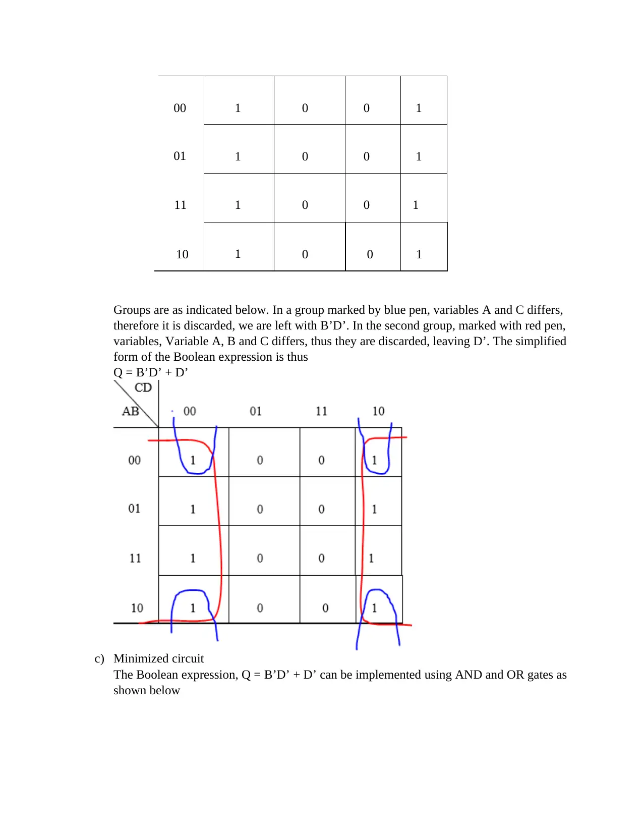
00
01
1 0 0 1
1 0 0 1
11 1 0 0 1
10 1 0 0 1
Groups are as indicated below. In a group marked by blue pen, variables A and C differs,
therefore it is discarded, we are left with B’D’. In the second group, marked with red pen,
variables, Variable A, B and C differs, thus they are discarded, leaving D’. The simplified
form of the Boolean expression is thus
Q = B’D’ + D’
c) Minimized circuit
The Boolean expression, Q = B’D’ + D’ can be implemented using AND and OR gates as
shown below
Paraphrase This Document
Need a fresh take? Get an instant paraphrase of this document with our AI Paraphraser
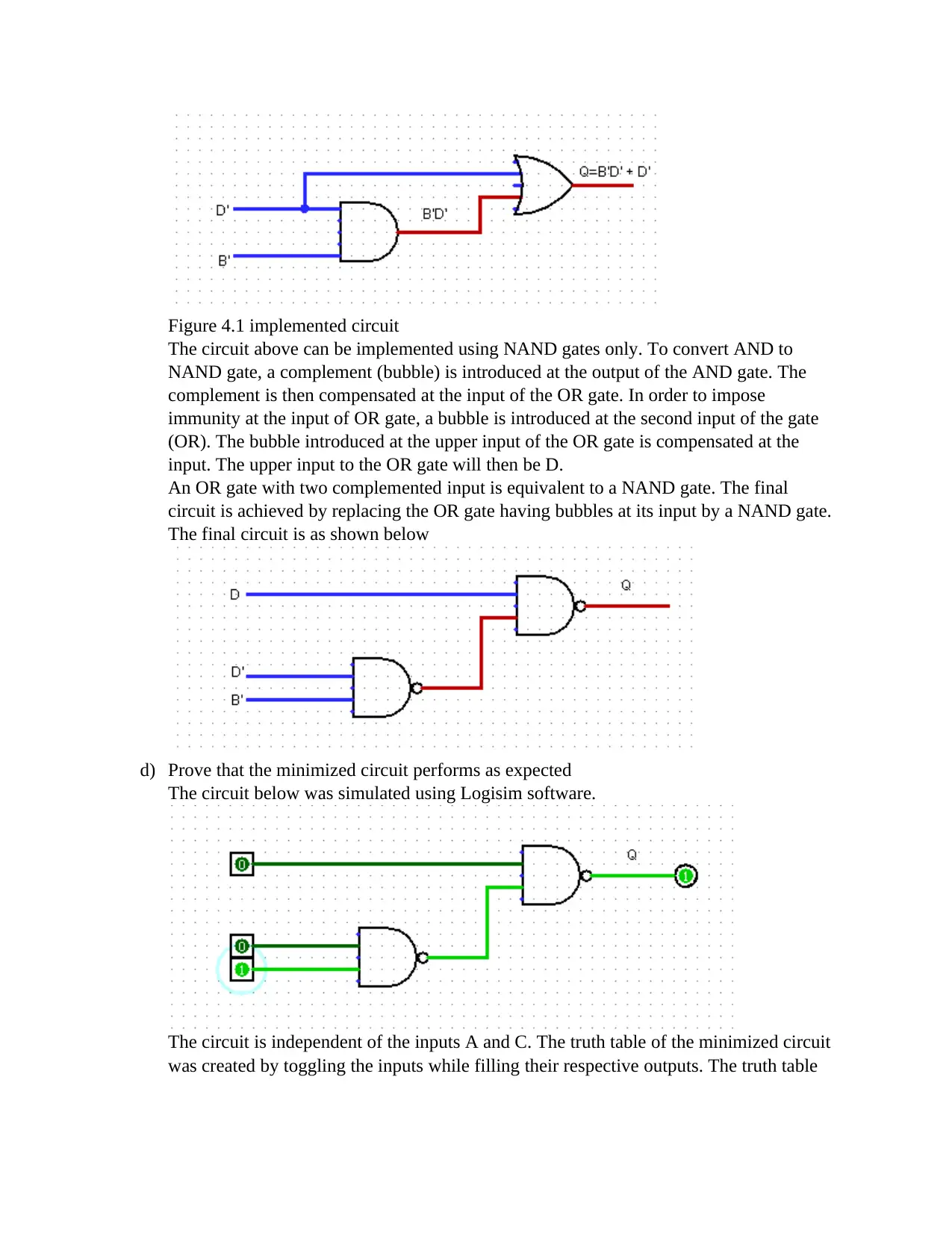
Figure 4.1 implemented circuit
The circuit above can be implemented using NAND gates only. To convert AND to
NAND gate, a complement (bubble) is introduced at the output of the AND gate. The
complement is then compensated at the input of the OR gate. In order to impose
immunity at the input of OR gate, a bubble is introduced at the second input of the gate
(OR). The bubble introduced at the upper input of the OR gate is compensated at the
input. The upper input to the OR gate will then be D.
An OR gate with two complemented input is equivalent to a NAND gate. The final
circuit is achieved by replacing the OR gate having bubbles at its input by a NAND gate.
The final circuit is as shown below
d) Prove that the minimized circuit performs as expected
The circuit below was simulated using Logisim software.
The circuit is independent of the inputs A and C. The truth table of the minimized circuit
was created by toggling the inputs while filling their respective outputs. The truth table

derived from the minimized circuit is similar to the truth table in part a, this is a prove the
minimized circuit gives a similar output as the initial Boolean expression.
B D Q
0 0 1
0 1 0
1 0 1
1 1 0
minimized circuit gives a similar output as the initial Boolean expression.
B D Q
0 0 1
0 1 0
1 0 1
1 1 0
⊘ This is a preview!⊘
Do you want full access?
Subscribe today to unlock all pages.
Trusted by 1+ million students worldwide

REFERENCES
Bird, J.O. (2017) Electrical Circuit Theory and Technology. 6th edn. New York: Routledge.
ElectronicsTutorial, (n.d) Input interfacing circuits. Available from< https://www.electronics-
tutorials.ws/io/input-interfacing-circuits.html.> Accessed 29th March, 2020.
Hughes, E.,Hiley, J., Brown, K., and Mckenzie,S., (2012) Electrical and electronics Technology.
10th edn, London: pearson
Null, L and Lobur, J. (2015). Computer Organization and Architecture.2nd edn. Boston: Jones
and Bartlett.
1 out of 10

Your All-in-One AI-Powered Toolkit for Academic Success.
+13062052269
info@desklib.com
Available 24*7 on WhatsApp / Email
![[object Object]](/_next/static/media/star-bottom.7253800d.svg)
Unlock your academic potential
Copyright © 2020–2026 A2Z Services. All Rights Reserved. Developed and managed by ZUCOL.