Engineering Design Project: 4x1 MUX Design and Implementation
VerifiedAdded on 2023/01/11
|23
|4632
|53
Project
AI Summary
This engineering design project details the design, implementation, and analysis of a 4x1 Multiplexer (MUX). The project begins with design specifications, including stakeholder requirements, and progresses through project planning, utilizing techniques like critical path analysis. The design employs combinational logic gates (AND, NOT, OR) and is simulated using Multisim software. The project covers evaluation tools, design techniques, modeling, and technical solutions, including a gate-based approach for optimal speed and minimized area. Potential limitations, finished product specifications, and safety considerations are addressed. The design solution is modeled and tested, with a focus on thorough testing of all input conditions. Communication strategies and potential improvements are also discussed. The project concludes with an overview of the MUX's functionality, its design process, and its potential for future development. The project demonstrates a solid understanding of digital electronics and circuit design principles. The project also involves practical implementation and simulation using industry-standard software to validate the design.

Engineering design1
ENGINEERING DESIGN
By Name
Course
Instructor
Institution
Location
Date
ENGINEERING DESIGN
By Name
Course
Instructor
Institution
Location
Date
Paraphrase This Document
Need a fresh take? Get an instant paraphrase of this document with our AI Paraphraser
Engineering design2
Contents
Introduction.................................................................................................................................................2
TASK 1:......................................................................................................................................................3
Design Specification................................................................................................................................3
Stakeholder’s Design Brief......................................................................................................................4
Project Schedule......................................................................................................................................6
Planning Techniques...............................................................................................................................7
Critical path:............................................................................................................................................8
Current Industry Standards......................................................................................................................8
TASK 2.....................................................................................................................................................10
Evaluation tools.....................................................................................................................................10
Design Techniques................................................................................................................................10
Modelling of Design..............................................................................................................................11
Technical Solutions...............................................................................................................................11
Task 3........................................................................................................................................................12
Engineering Design:..............................................................................................................................12
Potential Limitations:............................................................................................................................15
Finished Product Specification..............................................................................................................16
Safety and Risk Management Issues......................................................................................................16
Product effectiveness.............................................................................................................................16
TASK 4.....................................................................................................................................................17
Design Solution.....................................................................................................................................17
Communication Strategies.....................................................................................................................19
Effective Communication strategy............................................................................................................19
Justify potential improvements for the design...........................................................................................19
Conclusion.................................................................................................................................................20

Engineering design3
Table of figures
Figure 1: Showing the circuit diagram of 4×1 MUX...................................................................................4
Figure 2: Showing the circuit diagram of 4*1 MUX designed and tested in Multisim................................6
Figure 3: Showing the Project Schedule......................................................................................................7
Figure 4: Showing state diagram...............................................................................................................14
Figure 5: Showing 4*1 MUX designed in MULTISIM..................................................................................19
List of tables
Table 1: Showing the truth table................................................................................................................14
Table 2: Showing Boolean equations........................................................................................................15
Table 3: Showing Boolean equations........................................................................................................15
Table 4: Showing Boolean equations........................................................................................................15
Table 5: Showing Boolean equations........................................................................................................16
⊘ This is a preview!⊘
Do you want full access?
Subscribe today to unlock all pages.
Trusted by 1+ million students worldwide

Engineering design4
Introduction
A multiplexer (MUX) is a digital electronic device which allows one or several low speed
/ digital signal at the input to be selected, transmitted and also combined at a higher speed on one
shared medium. Therefore many inputs may share one device or transmission wire like copper or
aluminium or even optic fibre. Hence MUX operates as multiple input and single output. Some
key design specification must be employed to help realize the exact required product after the
design. The design specifications given will be compared with the stakeholders´ specifications to
help design and produce a product which will operate even better than those which are already in
the market. And before the design is conducted there must be a project plan to help give the best
designs well the construction of the real/ actual prototype of the design.
MUX can be in different types depending on the input for example if the inputs are 2
then it will be known as 2 channel or 2×1. If the inputs are 4 like the one we designed it will be
known as 4 channels or simply 4×1 and it can be illustrated below;
Paraphrase This Document
Need a fresh take? Get an instant paraphrase of this document with our AI Paraphraser
Engineering design5
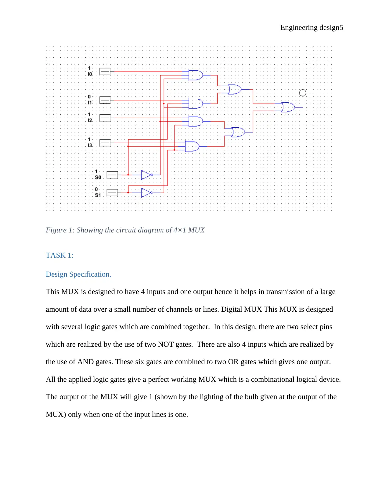
Figure 1: Showing the circuit diagram of 4×1 MUX
TASK 1:
Design Specification.
This MUX is designed to have 4 inputs and one output hence it helps in transmission of a large
amount of data over a small number of channels or lines. Digital MUX This MUX is designed
with several logic gates which are combined together. In this design, there are two select pins
which are realized by the use of two NOT gates. There are also 4 inputs which are realized by
the use of AND gates. These six gates are combined to two OR gates which gives one output.
All the applied logic gates give a perfect working MUX which is a combinational logical device.
The output of the MUX will give 1 (shown by the lighting of the bulb given at the output of the
MUX) only when one of the input lines is one.
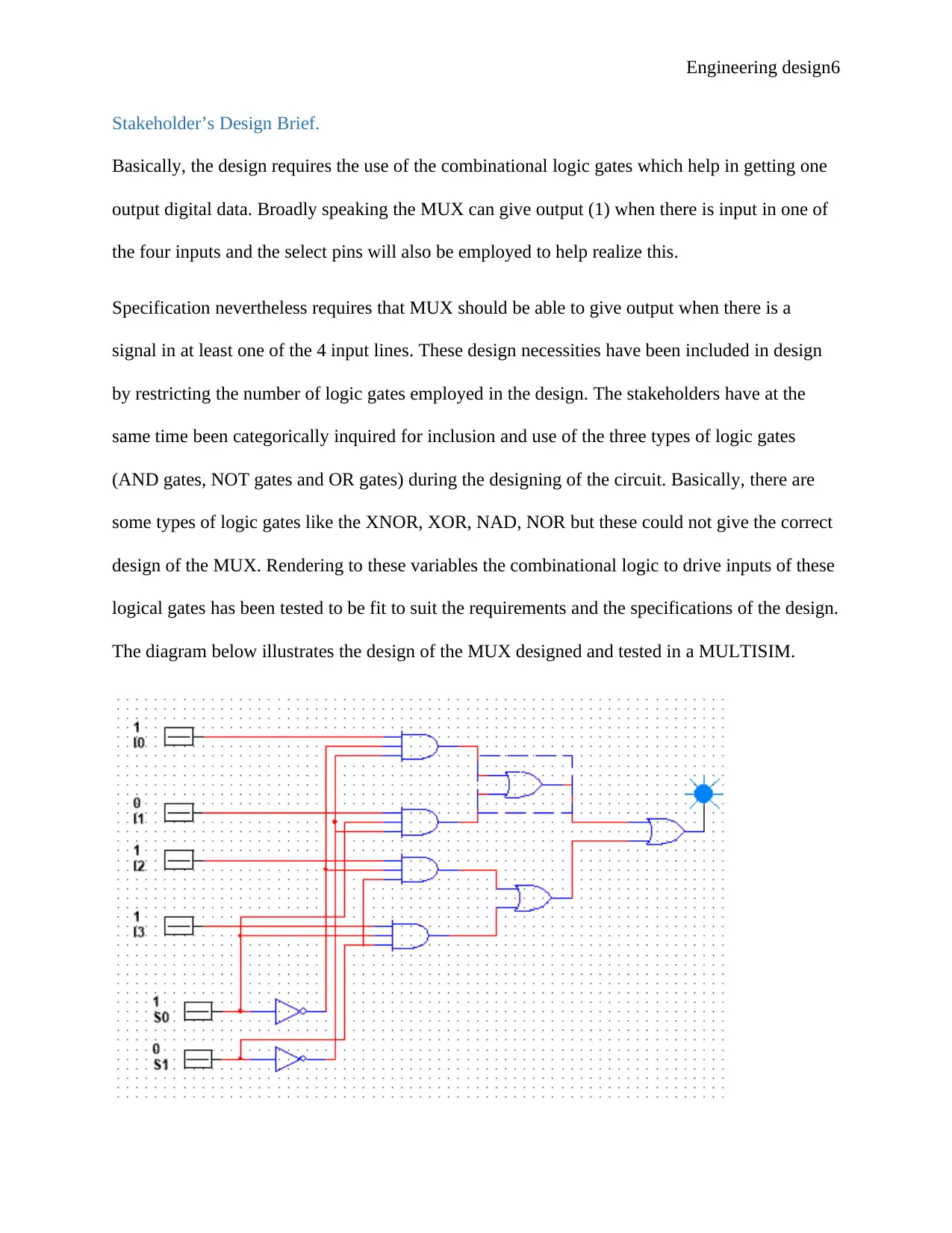
Engineering design6
Stakeholder’s Design Brief.
Basically, the design requires the use of the combinational logic gates which help in getting one
output digital data. Broadly speaking the MUX can give output (1) when there is input in one of
the four inputs and the select pins will also be employed to help realize this.
Specification nevertheless requires that MUX should be able to give output when there is a
signal in at least one of the 4 input lines. These design necessities have been included in design
by restricting the number of logic gates employed in the design. The stakeholders have at the
same time been categorically inquired for inclusion and use of the three types of logic gates
(AND gates, NOT gates and OR gates) during the designing of the circuit. Basically, there are
some types of logic gates like the XNOR, XOR, NAD, NOR but these could not give the correct
design of the MUX. Rendering to these variables the combinational logic to drive inputs of these
logical gates has been tested to be fit to suit the requirements and the specifications of the design.
The diagram below illustrates the design of the MUX designed and tested in a MULTISIM.
⊘ This is a preview!⊘
Do you want full access?
Subscribe today to unlock all pages.
Trusted by 1+ million students worldwide
Engineering design7
Figure 2: Showing the circuit diagram of 4*1 MUX designed and tested in Multisim
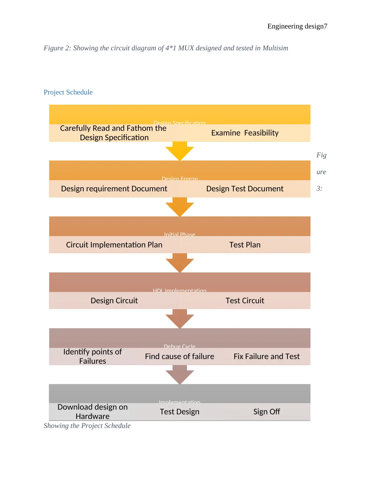
Project Schedule
Fig
ure
3:
Showing the Project Schedule
Implementation
Download design on
Hardware Test Design Sign Off
Debug Cycle
Identify points of
Failures Find cause of failure Fix Failure and Test
HDL Implementation
Design Circuit Test Circuit
Initial Phase
Circuit Implementation Plan Test Plan
Design Freeze
Design requirement Document Design Test Document
Design Specification
Carefully Read and Fathom the
Design Specification Examine Feasibility
Figure 2: Showing the circuit diagram of 4*1 MUX designed and tested in Multisim
Project Schedule
Fig
ure
3:
Showing the Project Schedule
Implementation
Download design on
Hardware Test Design Sign Off
Debug Cycle
Identify points of
Failures Find cause of failure Fix Failure and Test
HDL Implementation
Design Circuit Test Circuit
Initial Phase
Circuit Implementation Plan Test Plan
Design Freeze
Design requirement Document Design Test Document
Design Specification
Carefully Read and Fathom the
Design Specification Examine Feasibility
Paraphrase This Document
Need a fresh take? Get an instant paraphrase of this document with our AI Paraphraser
Engineering design8
Planning Techniques
The technique followed for the product is based on utilizing computers for simulating the
design before the real item is made on hardware. Typically a widely utilized approach within the
industry. The most preferences of the approach are decreased time in the redesign of the product
in case of unexpected possibility issues. The design in HDL implementation stage can capture a
lot of issues that might come up in real design. The approach moreover permits designers to
make more than one design for the same circuit. Some choices make way for comparison of
diverse implementations and scrutiny of the advantages of one kind of design over the other
designs.
The later the adjustment in the design, the more expensive it is to oblige those adjustments in
design. Modelling based approach decreases this cost significantly. The issue with modelling
based approach is an incapacity to see the real item working in real circumstance. Regularly
modelling stages operate the model of the product model at much lower rates compared to what
they are anticipated to run at in real-world situation. This makes it essential to test the design not
only in demonstrating the environment but moreover in its real utilization scenario. It is actually
encouraged that the design is done in software then it is properly tested using the same software
until it works perfectly as anticipated to work1. This will help in reduces the costs that would
1 Zhang, Jingyun. 2010. Analysis and design of integrated, etched grating Dense Wavelength
Division Multiplexers. Beijing: Cornell University. https://books.google.co.ke/books?
id=C2BUAAAAYAAJ&q=design+of+MUX&dq=design+of+MUX&hl=en&sa=X&ved=0ahUKEwj4n8b
y_c3hAhXX63MBHe3DBcIQ6AEIXzAJ.
Zheng, Lizhen. 2017. High-speed Rapid-single-flux-quantum Multiplexer and Demultiplexer Design and
Testing. California: University of California, Berkeley. https://books.google.co.ke/books?
id=zq9PAQAAMAAJ&q=design+of+MUX&dq=design+of+MUX&hl=en&sa=X&ved=0ahUKEwj4n8b
y_c3hAhXX63MBHe3DBcIQ6AEIUzAH.
Engineering design9
have been incurred if the actual device was constructed without having the model simulated and
check the errors. The use of the model and computer simulations also help a lot in saving the
time which would have been wasted when the real product was fabricated and it had an error. As
this will imply that another product will be constructed again and again until the one which has
the required specifications is made. In most cases, this cannot be realized due to errors of a
human. Therefore it is very important to simulate before constructing the real product.
Critical path:
For every serious project done like this, there are several small activities which are done to help
realize the overall objective of designing the overall product with the required specifications.
Each activity has its own goals and its requirements for inputs. Sometimes the output of one
activity is input to the other activity. When the previous task is not completed on time, it affects
the starting time of the following activity. Depending upon delays in activity completion, the
task might become the bottleneck for the project to progress further. The Critical Path Method is
defined in the Project Management Body of Knowledge (PMBOK) as follows: “The Critical
Path”
The method is the sequence of scheduled activities that determines the duration of the
project." Any project has a set of activities that are critical and some are non –critical.
This too may change during the execution of the project that a few exercises that were at
first non-critical have currently become critical in the sense that their completion is holding up
⊘ This is a preview!⊘
Do you want full access?
Subscribe today to unlock all pages.
Trusted by 1+ million students worldwide
Engineering design10
the progress of the project and must be performed urgently in case the project is to be completed
effectively. Basic path recognizes the chain of assignments that must be completed precisely on
time to avoid project from getting postponed.
Current Industry Standards
The present design has the specification as given in the stakeholder's necessity document.
There are several variations of the same circuit present in the market which permits from extra
functionality to the design at added cost and size of the designed product2. Future versions of the
product can be expected to have that some other functionality like parallel load, reset and hold
functions when there is a need. Actually, these extra functionalities will enable the product to
operate better than the current products which are in the market. These functionalities will even
attract more customers to buy them over the current products already in the market.
2 Sachdev, Manoj. 2018. CMOS SRAM Circuit Design and Parametric Test in Nano-Scaled
Technologies: Process-Aware SRAM Design and Test. Sydney: Springer Science & Business
Media. https://books.google.co.ke/books?
id=OXigu7wLa34C&dq=design+of+MUX&source=gbs_navlinks_s.
Vahid, Frank. 2010. Digital Design with RTL Design, Verilog and VHDL. Hull: John Wiley & Sons.
https://books.google.co.ke/books?id=-
YayRpmjc20C&dq=design+of+MUX&source=gbs_navlinks_s.
Paraphrase This Document
Need a fresh take? Get an instant paraphrase of this document with our AI Paraphraser
Engineering design11
TASK 2
Evaluation tools
As per now there a lot of software which can be employed to make the design of this circuit, this
software can be applied for both large scale production and small scale production. Depending
on the user specifications any of the platforms can be employed. The platforms considered for
the current product development included Multisim from Nation Instruments, Orcad Pspice from
Cadence and open source software like Logisim and Logically. But for this project, Multisim
software was used for the development and testing of the device as it is a standard and reliable
software. This is because it is very easy to use Multisim in designing this circuit diagram and test
for the operation of the 4×1 MUX. The circuit diagram obtained from Multisim is can be
illustrated in figure 1 above.
Design Techniques
Standard design strategies are followed when designing the system utilizing digital
components present in the market with demonstrated functionality and determination. Once all
states and their transitions to another state are recognized, the diagram is mapped to a truth table
that shows the same data in the digital domain. The concluded truth table is then diminished to
useful Boolean equations in minimized form. Once the required equation is derived, the circuit is
designed in a simulation environment and tried thoroughly for all functional specifications.
When there is an error during testing then the error can be debugged (corrected) until we have
the final circuit diagram which operates as required by the designer.
Engineering design12
Modelling of Design
The design solution created is modelled and tested in Multisim software utilizing
standard library components which are in place tab of the software. The inputs expected for the
circuit are emulated utilizing available gadgets3. All possible input conditions for changing time
lengths are tested on the circuit. Once all conditions are checked and confirmed to be in the state
as required, the circuit is considered mature for another stage is implementation. The simulation
included connecting logic gates in the circuit at the posedge of it. The inputs which are AND
gates are connected to their own combination circuits utilizing an arrangement of OR doors. The
control flag up/down is additionally driven as a portion of the testbench.
Technical Solutions
Currently, there are a lot of choices which can be employed to realize the functional
circuit using high-level components like ROM and MUX for the combinational part of the
design. Nevertheless, individual gate based approach was used as it was most effective in terms
of the logic gate and minimized area and optimized speed. Cost of design using gates was also
less compared to high-level design components. So a gate based design was deduced and
implemented. And for every design of the large scale production cost of the design must be
3 Bertacco, Valeria. 2018. Functional Design Errors in Digital Circuits: Diagnosis Correction and
Repair. London: Springer Science & Business Media. https://books.google.co.ke/books?
id=S8fUrOUOx0AC&dq=design+of+MUX&source=gbs_navlinks_s.
Berube, Richard. 2014. Computer Simulated Experiments for Digital Electronics Using Electronics
Workbench Multisim. Stoke: Prentice Hall PTR. https://books.google.co.ke/books?id=-
6vWAAAAMAAJ&dq=Digital+electronic+design+in+MULTISIM,&hl=en&sa=X&ved=0ahUKEwjL_O
C3g87hAhWCk4sKHd2nA74Q6AEINTAC.
⊘ This is a preview!⊘
Do you want full access?
Subscribe today to unlock all pages.
Trusted by 1+ million students worldwide
1 out of 23
Related Documents


Your All-in-One AI-Powered Toolkit for Academic Success.
+13062052269
info@desklib.com
Available 24*7 on WhatsApp / Email
![[object Object]](/_next/static/media/star-bottom.7253800d.svg)
Unlock your academic potential
Copyright © 2020–2026 A2Z Services. All Rights Reserved. Developed and managed by ZUCOL.