Analysis of MIS Memory Devices: Fabrication, Measurements, and Results
VerifiedAdded on 2023/04/20
|10
|2139
|231
Report
AI Summary
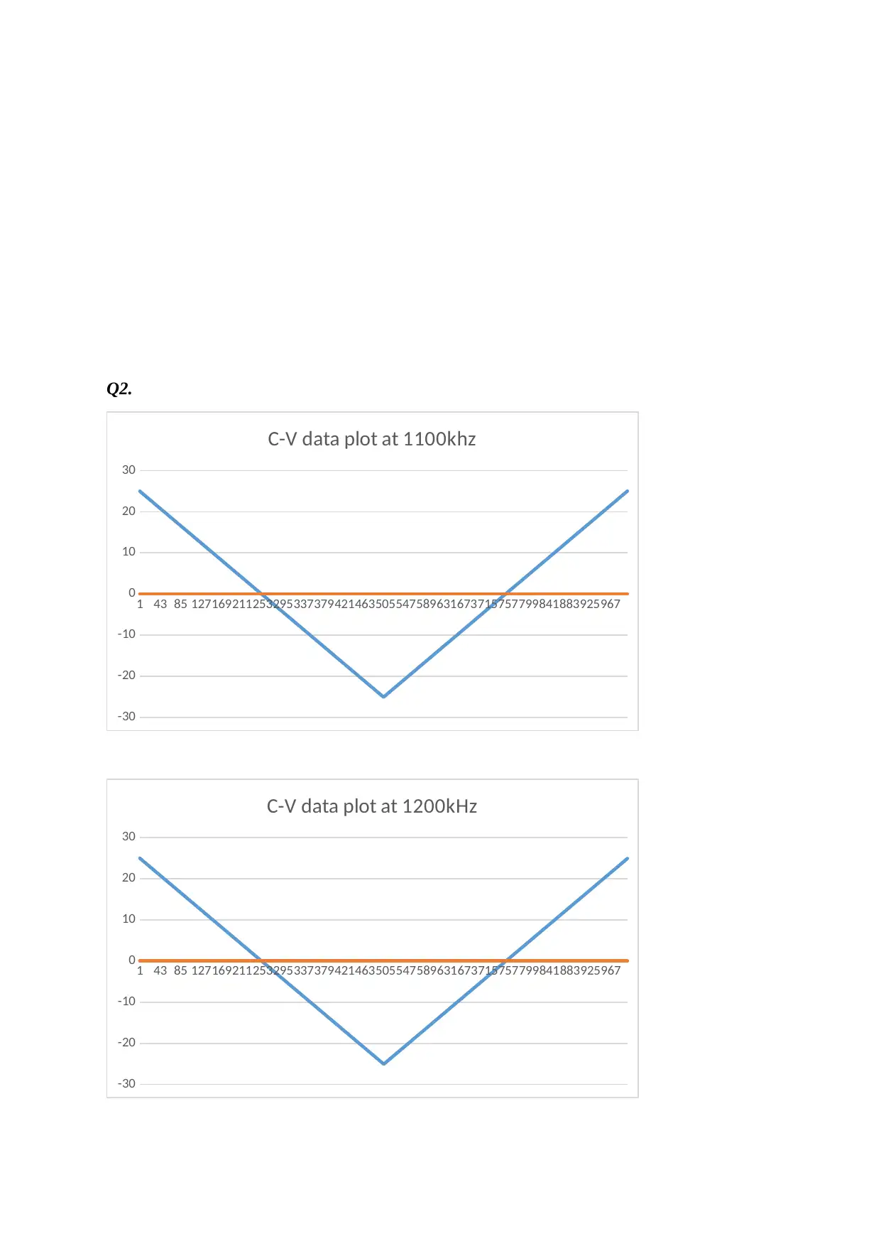
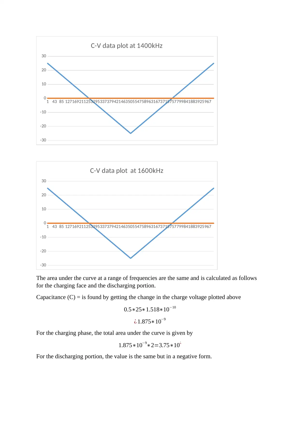
This report presents a detailed analysis of Metal-Insulator-Semiconductor (MIS) memory devices, focusing on their fabrication and electrical characterization. The study begins with an introduction to memory devices, differentiating between volatile and non-volatile types and highlighting their applications. The core of the report describes the fabrication process, including the use of a silicon substrate, cleaning procedures, and the deposition of thin oxide layers, aluminum contacts, and silicon nanostructures, which act as floating gates. The report then delves into the electrical measurements, specifically analyzing capacitance-voltage (C-V) data at various frequencies to assess charge storage and discharge characteristics within the semiconductor. The C-V data is used to calculate the area under the curve for various frequencies, and the charge is calculated for the memory devices. Retention data plots are presented to illustrate the behavior of the memory device in zero and one states, emphasizing the role of the nanostructure floating gate in data retention. The report concludes with a discussion of flash memory technology, comparing single-level and multi-level cells and addressing the advantages of using nanostructures for improved data security and device performance. The report also provides fabrication procedures and analysis of test outcomes, which are then summarized and analyzed for their effectiveness and efficiency.
Contribute Materials
Your contribution can guide someone’s learning journey. Share your
documents today.

Physics of Semiconductor Devices
Institution Name:
Student Name:
Institution Name:
Student Name:
Secure Best Marks with AI Grader
Need help grading? Try our AI Grader for instant feedback on your assignments.

Abstract
Currently, most memory devices increasingly play important role in microelectronics
technology and considered as the technology drivers, whereas electronic memories cover up
to 20% of semiconductors available in the market. Ideally, these memory devices are divided
into two types, for example, volatile memories and non-volatile memories. The speed of
write-erase operations in volatile memories such as SRAM and DRAM are very high, while
these memories will lose data when the supply voltage is removed. In contrast, nonvolatile
memories have a very low write-erase speed with the need for high voltage and longer
retention time, usually more than 10 years.
These different types of memories have different functions or in other words, fill a particular
function in a particular system. For example, SRAM memories are used by microprocessors
of computers as off-chip or on-chip cache to store copies of memory locations that are most
frequently used, to reduce the memory access time average. Compared to other types of
volatile memories SRAM memories are expensive and tend to have a high write-erase speed
than DRAMs. DRAM memories provide random access storage when used in main memory
computers that make them relatively large and cheap as compared to static RAMs and this
makes them faster as compared to non-volatile memories
Introduction.
The MIS fabrication process will be undertaken using various available equipment in the
EMTERC research group [1]. A p-type semiconductor made up of a silicon substrate,
containing a thin native oxide (1-2 nm) will be provided. A standard organic solvent cleaning
procedure is used to perform the cleaning of the silicon wafer.to establish ohmic contact,
Aluminium and annealing are evaporated in nitrogen at five hundred degrees Celsius by
performing the bottom contact. The Sn coating of the silicon wafer on the polished side, of

thickness 3 nm (approximately), by thermal evaporation. This is then followed by deposition
of Si nanostructures (a floating gate in the above schematic diagram). The Device is
completed by deposition of the silicon nitride layer and top aluminium contact. A reference
sample, without the deposition Sn and silicon nanostructures, will also be fabricated at the
same time [2].
Results and Discussions
Q1.
Metal-insulator-semiconductor has a thin insulating layer that allows a given amount of
current known as the tunnel current to flow between metal and semiconductor and causes the
semiconductor to depart from the thermal equilibrium. The diode has a negatively charged
source of electric charges and a positively charged control gate that helps in creating the
potential for the flow of electrons. For flash memory with a nanostructure as the floating gate,
the negative and the positive electric charges which exist at the source and the control gate
respectively helps to draw electrons into the Nanostructure floating gate. Semiconductor
fabricated Flash memories works by charging or discharging electrons to and from a floating
gate. A bit's zero or one state depends upon whether or not the Nanostructure floating gate is
charged or uncharged. Due to the presence of electrons on the floating gate, tunnel current
can't flow through the semiconductor transistor and the bit state is Zero. This defines the
normal state for a Nanostructure floating gate transistor when a bit is programmed. When
electrons are removed from the floating gate, current is allowed to flow and the bit state is
one. [3].

Q2.
1 43 85 127169211253295337379421463505547589631673715757799841883925967
-30
-20
-10
0
10
20
30
C-V data plot at 1100khz
1 43 85 127169211253295337379421463505547589631673715757799841883925967
-30
-20
-10
0
10
20
30
C-V data plot at 1200kHz
1 43 85 127169211253295337379421463505547589631673715757799841883925967
-30
-20
-10
0
10
20
30
C-V data plot at 1100khz
1 43 85 127169211253295337379421463505547589631673715757799841883925967
-30
-20
-10
0
10
20
30
C-V data plot at 1200kHz
Secure Best Marks with AI Grader
Need help grading? Try our AI Grader for instant feedback on your assignments.

1 43 85 127169211253295337379421463505547589631673715757799841883925967
-30
-20
-10
0
10
20
30
C-V data plot at 1400kHz
1 43 85 127169211253295337379421463505547589631673715757799841883925967
-30
-20
-10
0
10
20
30
C-V data plot at 1600kHz
The area under the curve at a range of frequencies are the same and is calculated as follows
for the charging face and the discharging portion.
Capacitance (C) = is found by getting the change in the charge voltage plotted above
0.5∗25∗1.518∗10−10
¿ 1.875∗10−9
For the charging phase, the total area under the curve is given by
1.875∗10−9∗2=3.75∗10¿
For the discharging portion, the value is the same but in a negative form.
-30
-20
-10
0
10
20
30
C-V data plot at 1400kHz
1 43 85 127169211253295337379421463505547589631673715757799841883925967
-30
-20
-10
0
10
20
30
C-V data plot at 1600kHz
The area under the curve at a range of frequencies are the same and is calculated as follows
for the charging face and the discharging portion.
Capacitance (C) = is found by getting the change in the charge voltage plotted above
0.5∗25∗1.518∗10−10
¿ 1.875∗10−9
For the charging phase, the total area under the curve is given by
1.875∗10−9∗2=3.75∗10¿
For the discharging portion, the value is the same but in a negative form.

1 43 85 127169211253295337379421463505547589631673715757799841883925967
-30
-20
-10
0
10
20
30
C-V data plot at 1800kHz
The above graphic plots indicate the capacitance-Voltage representation of the charging and
discharging process in semiconductors during the fabrication of the memory devices. The
charge storage and discharge data plotted was taken at different frequencies of electrical
charge and discharge.
The purpose of the range of frequencies was to verify the difference in data loss and
efficiency of operation of the floating gate during the movement of the charges at zero and
one states.
The data obtained is the same for different frequencies as shown above. This shows that the
semiconductors operate normally and the capacitance in the same for both higher and lower
frequencies especially when the devices are containing a nanostructure which forms the
floating gate.
Q.3.
CV data used to calculate the area under the CV plots above can be used to find the charge
storage in the memory devices as shown below. Also as observed that the area under the CV
curves above is the same at all frequencies, we will use one frequency to evaluate the charge
in the memory devices.

We take a frequency of 1100kHz
Charge= Area under the curve*the frequency
For the charging phase
Charge = 3.75∗10−9∗1100∗103
¿ 4.125∗10−3 coulombs
Q4.
The figure above represents the retention plot of a MIC memory device with a silicon
nanostructure in it as the floating gate. During the zero states, the memory does not contain
any data within it thus the measured values are only for the electrical charge signals. While
during the 1 state the information contained in the memory device moves together with the
1 8 15 22 29 36 43 50 57 64 71 78 85 92 99 106 113 120 127 134 141 148 155 162
-25
-20
-15
-10
-5
0
5
10
15
20
25
Retention Data Plot for 0 and 1 states
Paraphrase This Document
Need a fresh take? Get an instant paraphrase of this document with our AI Paraphraser

charges and are being retained within the same period of time as that over which the charges
are contained before being discharged [6].
Q5.
Flash memory consisting of an array of memory cells, each memory cell makes up one
floating gate transistor which makes it capable of storing at least one bit. Multi-level cells
allow for the storage of more than one bit per cell by choosing between multiple levels of
electrical charge in the floating gate of a cell, while single-level cells are able to store only
one bit of information per cell [7].
Metal-Insulator semiconductors are made of silicon devices that contains nona structures
forming a floating gate. The electrical charges that contain data in flash memories move from
the source gate and are temporarily being stored in the floating gate before finally being
discharged. The data security in flash memories especially those operating with silicon
semiconductors is not guaranteed. This poses a disadvantage since there may be critical
information contained and that can be lost when the charges are lost before the correct
destination [8].
The use of Nanostructures will eliminate the problem of data loss. The floating gate formed
by the Nanostructures helps to hold the data until all the information that was required from it
is fully utilized. Also, the would be little damages to the structure and alignment since the
distance to the discharge point is greatly reduced by the Nanostructures [9].
Conclusions and Future Scope
An electrically characterize Metal-Insular-Semiconductor structures containing silicon nano-
structures was successfully fabricated from a selected catalyst (tin) as a charge storing
element [10].

Testing was done and measurements were taken at different frequencies and Capacitance
Voltage diagrams are drawn to analyze the behaviour of the flash memory with
nanostructures at different frequencies. Fabrication procedure is shown and the data given for
various test outcomes [11].
The future scope of the semiconductor technology as far as the memory devices are
concerned is an open area of research and study. More work should be done in ensuring more
secure information and accurate memory devices can be fabricated. Floating gates with other
materials or more advanced nanostructures can be used for this [12].
References
[1] K. Nam- Goo, C. Byungjin, K. Beom- Goo, S. Sunghoon, L. Takhee, and Jae- Suk,
"Memory Devices: Structural and Electrical Characterization of a Block Copolymer-
Based Unipolar Nonvolatile Memory Device," vol. 24, p. 1, 2012.
[2] E. Abdurakhmanov, L. Ykhshilikova, and Z. Murodova, "Development of the
semiconductor analyzer for the control steam ethanol," European Journal of analytical
and applied chemistry, p. 03, 2015.
[3] Yoo, J. Eun, Lyu, Xiao Qiang, Yun, Jung- Ho, Kang, J. Chi, Choi, J. Young, Wang and
Lianzhou, "Memory Devices: Resistive Switching Behavior in Organic-Inorganic
Hybrid CH 3 NH 3 PbI 3 −x Clx Perovskite for Resistive Random Access Memory
Devices," Journal of Advanced Materials, vol. 27, p. 1, 2015.
[4] C. Seongjae, K. Yoon, Y. Jang- Gn, H. L. Jung, B. S. Won, and P. Byung- Gook,
"Dependence of program and erase speed on bias conditions for the fully depleted
channel of vertical NAND flash memory devices," 10th Annual Non-Volatile Memory
Technology Symposium, p. 03, 2009.
[5] Huang, Y. Sheng, Chang, Tiang- Chang, Chen, Min- Chen, M. Simon, Tsai, and Min-
Jinn, "Volatile Memory Technology Symposium Proceeding - Investigation of resistive
switching properties in Sm2O3 memory devices," 11th Annual Non-Volatile Memory

Technology Symposium (NVMTS), p. 03, 2011.
[6] M. Wagner, H. Schneider, D. Stehr, S. Winnerl, M. R. Helm, A. M. Andrews, S.
Shartner and G. Strasser, "Terahertz Induced Intra-excitonic Autler-Townes Effect In
Semiconductor Quantum Wells," 30th International Conference on the Physics of
Semiconductors, p. 2, 2011.
[7] Tian, Zhao, Haiming, Wang, Xue- Feng, Qian- Yi, Hong- Yu, Mohammad, and A.
Mohammad, "Memory Devices: In Situ Tuning of Switching Window in a Gate-
Controlled Bilayer Graphene-Electrode Resistive Memory Device," Journal of
Advanced Materials, vol. 27, p. 1, 2015.
[8] Kim, W. Hyun, You, H. Joo, Lee, U. Dea, Kim, W. Tae, Lee and W. Keun,
"Enhancement of the device characteristics for nanoscale charge trap flash memory
devices utilizing a metal spacer layer," International Conference on Simulation of
Semiconductor Processes and Devices, p. 4, 2011.
[9] Das, Ne, Xue and Wang, "Electrical characterization of resistive memory in metal,"
10th Annual Non-Volatile Memory Technology Symposium, p. 20, 2009.
[10] L. Chih-yuan, L. HangTing and C. Yichou, "State-of-the-art flash memory devices and
post-flash emerging memories," Science China Information Sciences, vol. 54, p. 22,
2011.
[11] C. Byungjin, S. Sunghun, J. Yongsung, K. Tae- Wook and L. Tokhee, "Memory
Devices: Organic Resistive Memory Devices: Performance Enhancement, Integration,
and Advanced Architectures," Journal of Advanced Mechanics, vol. 21, p. 1, 2011.
[12] Yacomotti, M. Alejandro, Haddadi, Samir, Sagnes, Isabelle, Raineri, Fabrice, Levenson
and J. Ariel, "Efficient free space coupling in a 2D semiconductor photonic crystal
nanocavities," 14th International Conference on Transparent Optical Networks
(ICTON), p. 04, 2012.
1 out of 10

Your All-in-One AI-Powered Toolkit for Academic Success.
+13062052269
info@desklib.com
Available 24*7 on WhatsApp / Email
Unlock your academic potential
© 2024 | Zucol Services PVT LTD | All rights reserved.