Analysis of Negative and Positive Feedback in Electronic Circuits
VerifiedAdded on 2022/08/21
|9
|1331
|42
Report
AI Summary
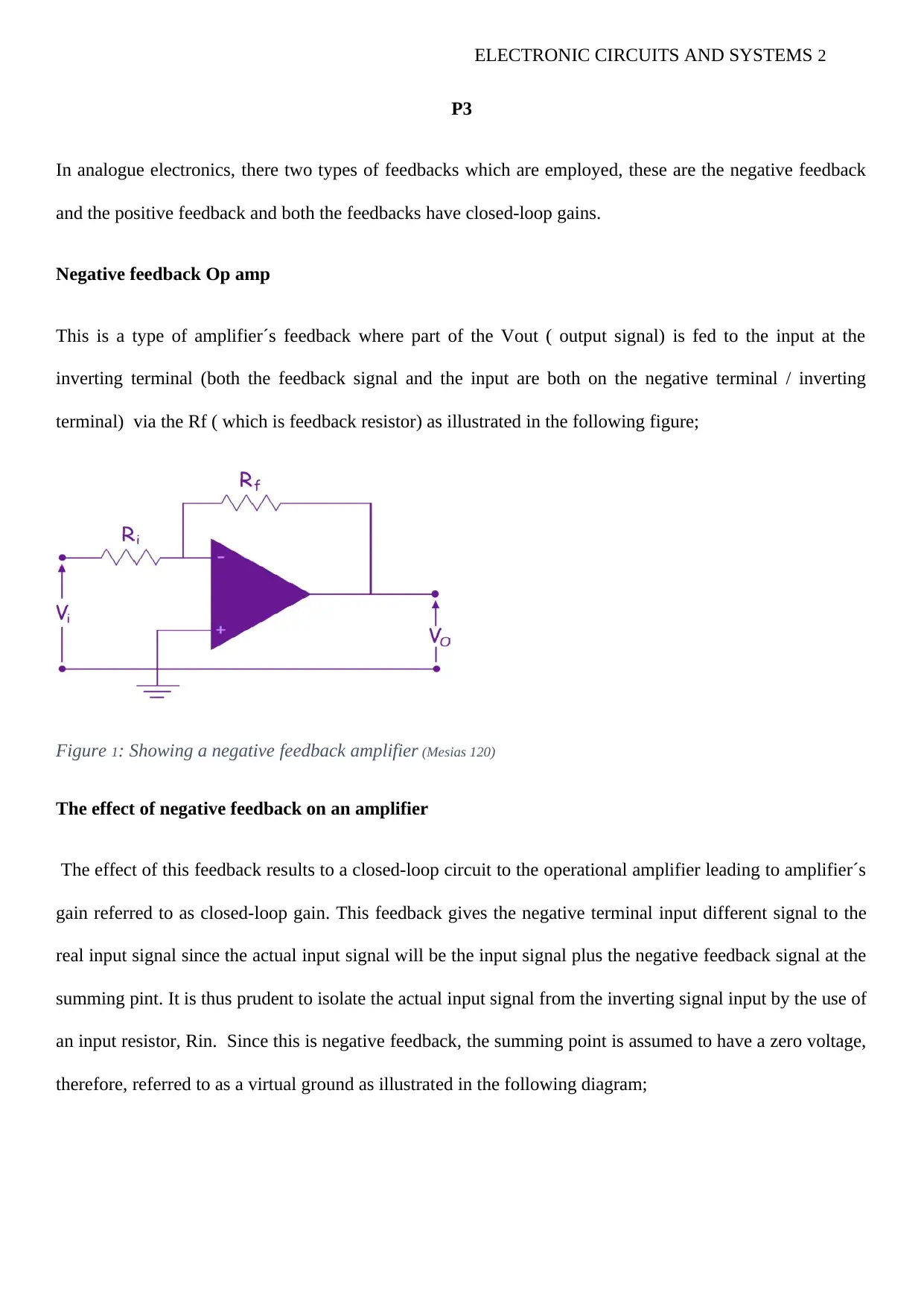
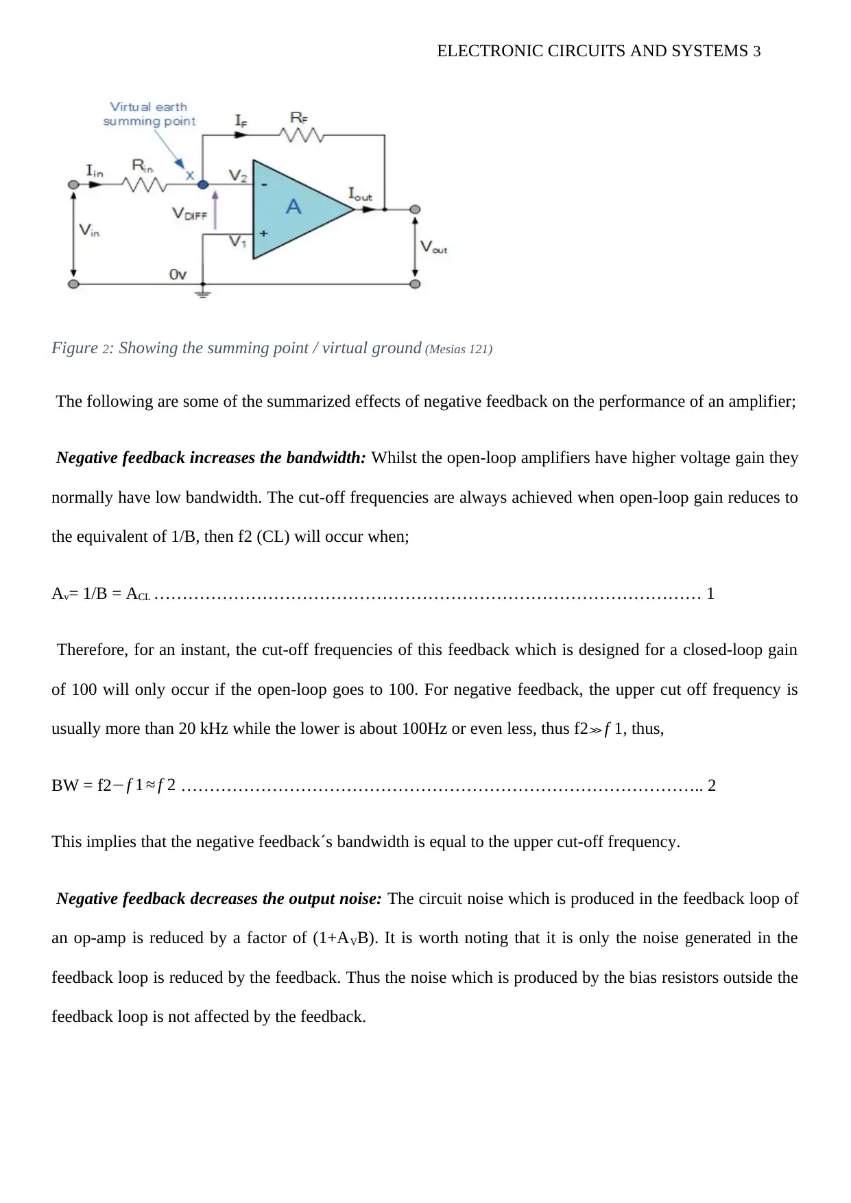
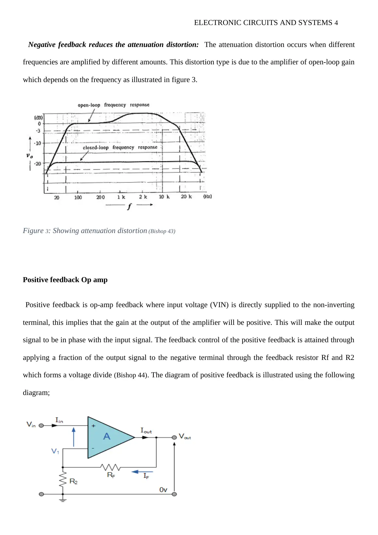
This report provides a detailed analysis of negative and positive feedback in electronic circuits and systems. It begins by defining and differentiating between negative and positive feedback, explaining their effects on amplifier performance, including closed-loop gain, bandwidth, and distortion. The report then delves into the specifics of negative feedback, detailing its impact on bandwidth and noise reduction, and also examines how positive feedback increases closed-loop gain and reduces bandwidth. Furthermore, the report discusses practical applications, such as the differentiator circuit, illustrating how negative feedback principles are applied. The analysis includes circuit diagrams, equations, and waveform examples to support the theoretical concepts, making it a comprehensive resource for understanding the behavior and application of feedback mechanisms in electronic circuits. The report also cites relevant literature, including Bishop's 'Electronics - Circuits and Systems' and Mesias' 'Electronics: Theory and Practice' to substantiate the analysis.

ELECTRONIC CIRCUITS AND SYSTEMS 1
ELECTRONIC CIRCUITS AND SYSTEMS
By Name
Course
Instructor
Institution
Location
Date
ELECTRONIC CIRCUITS AND SYSTEMS
By Name
Course
Instructor
Institution
Location
Date
Paraphrase This Document
Need a fresh take? Get an instant paraphrase of this document with our AI Paraphraser

ELECTRONIC CIRCUITS AND SYSTEMS 2
P3
In analogue electronics, there two types of feedbacks which are employed, these are the negative feedback
and the positive feedback and both the feedbacks have closed-loop gains.
Negative feedback Op amp
This is a type of amplifier´s feedback where part of the Vout ( output signal) is fed to the input at the
inverting terminal (both the feedback signal and the input are both on the negative terminal / inverting
terminal) via the Rf ( which is feedback resistor) as illustrated in the following figure;
Figure 1: Showing a negative feedback amplifier (Mesias 120)
The effect of negative feedback on an amplifier
The effect of this feedback results to a closed-loop circuit to the operational amplifier leading to amplifier´s
gain referred to as closed-loop gain. This feedback gives the negative terminal input different signal to the
real input signal since the actual input signal will be the input signal plus the negative feedback signal at the
summing pint. It is thus prudent to isolate the actual input signal from the inverting signal input by the use of
an input resistor, Rin. Since this is negative feedback, the summing point is assumed to have a zero voltage,
therefore, referred to as a virtual ground as illustrated in the following diagram;

ELECTRONIC CIRCUITS AND SYSTEMS 3
Figure 2: Showing the summing point / virtual ground (Mesias 121)
The following are some of the summarized effects of negative feedback on the performance of an amplifier;
Negative feedback increases the bandwidth: Whilst the open-loop amplifiers have higher voltage gain they
normally have low bandwidth. The cut-off frequencies are always achieved when open-loop gain reduces to
the equivalent of 1/B, then f2 (CL) will occur when;
Av= 1/B = ACL …………………………………………………………………………………… 1
Therefore, for an instant, the cut-off frequencies of this feedback which is designed for a closed-loop gain
of 100 will only occur if the open-loop goes to 100. For negative feedback, the upper cut off frequency is
usually more than 20 kHz while the lower is about 100Hz or even less, thus f2≫ f 1, thus,
BW = f2−f 1 ≈ f 2 ……………………………………………………………………………….. 2
This implies that the negative feedback´s bandwidth is equal to the upper cut-off frequency.
Negative feedback decreases the output noise: The circuit noise which is produced in the feedback loop of
an op-amp is reduced by a factor of (1+AVB). It is worth noting that it is only the noise generated in the
feedback loop is reduced by the feedback. Thus the noise which is produced by the bias resistors outside the
feedback loop is not affected by the feedback.
⊘ This is a preview!⊘
Do you want full access?
Subscribe today to unlock all pages.

Trusted by 1+ million students worldwide

ELECTRONIC CIRCUITS AND SYSTEMS 4
Negative feedback reduces the attenuation distortion: The attenuation distortion occurs when different
frequencies are amplified by different amounts. This distortion type is due to the amplifier of open-loop gain
which depends on the frequency as illustrated in figure 3.
Figure 3: Showing attenuation distortion (Bishop 43)
Positive feedback Op amp
Positive feedback is op-amp feedback where input voltage (VIN) is directly supplied to the non-inverting
terminal, this implies that the gain at the output of the amplifier will be positive. This will make the output
signal to be in phase with the input signal. The feedback control of the positive feedback is attained through
applying a fraction of the output signal to the negative terminal through the feedback resistor Rf and R2
which forms a voltage divide (Bishop 44). The diagram of positive feedback is illustrated using the following
diagram;
Paraphrase This Document
Need a fresh take? Get an instant paraphrase of this document with our AI Paraphraser

ELECTRONIC CIRCUITS AND SYSTEMS 5
Figure 4: Showing positive feedback (Mesias 123)
The effect of positive feedback on the amplifier
Unlike the negative feedback, in a positive feedback amplifier, the feedback signal being fed to the system
is of the same phase. Below are some common ways in which positive feedback can affect the performance
of the amplifier;
There is increased in closed-loop gain (closed-loop gain is higher) for the positive feedback
Since the signal being fed back to the circuit is in phase with the input, the overall gain will be higher than
that of the negative feedback. Mathematically, the closed-loop gain of positive feedback is given by the
following equation;
loopgain=1+ R 1
R 2 ……………………………………………………………………………….. 3
For the amplifier's stability, the value of R1 is always bigger than the value of R2, thus resulting in the
higher value of the closed-loop gain for the system.
The bandwidth is reduced in positive feedback:
The formula for the bandwidth in positive feedback is given by equation 4 below;
β= R 2
R 1+R 2 ………………………………………………………………………………… . . . . . 4
And since the gain is higher, it implies that the R1 is bigger than R2, thus equation 4 will result in a smaller
value. If we assume that gain is 20 and the required output is 10 v, then the required bandwidth can be
calculated from the following equation
Bandwidth = Cosntantoutput
gain

ELECTRONIC CIRCUITS AND SYSTEMS 6
Bandwidth = 10
20 = 0.5
And if we take gain is 40 at the same output of 10 (constant), bandwidth will be
Bandwidth = 10
40 = 0.25
Therefore from equation 4 above, it clearly shows that when the gain is increased the bandwidth is reduced
at the same output signal.
P 4
There are several circuits which employ the principles of negative feedback in their operation. For this
differentiator circuit will be used. This circuit uses a capacitor which is in series to the voltage input source
as illustrated in the following diagram;
Figure 5: Showing differentiator circuit (Mesias 123)
For the Direct current input, the input capacitor will remain unchanged and it will behave like an open
circuit to the DC current. The non-inverting input terminal of the circuit is connected to the ground via a
compensation resistor (Rcomp). The Rcomp will provide input bias compensation and the inverting terminal
is connected to the output via Rf (the feedback resistor). The capacitor will only allow the movement of AC
current to pass through and the frequency of that AC depends on the rate of change of the input signal. The
lower frequencies result in higher capacitor´s reactance which gives low gain ( Rf/Xc) and low voltage
output. When the frequency is higher the capacitive reactance is highly reduced leading to higher voltage
Bandwidth = 10
20 = 0.5
And if we take gain is 40 at the same output of 10 (constant), bandwidth will be
Bandwidth = 10
40 = 0.25
Therefore from equation 4 above, it clearly shows that when the gain is increased the bandwidth is reduced
at the same output signal.
P 4
There are several circuits which employ the principles of negative feedback in their operation. For this
differentiator circuit will be used. This circuit uses a capacitor which is in series to the voltage input source
as illustrated in the following diagram;
Figure 5: Showing differentiator circuit (Mesias 123)
For the Direct current input, the input capacitor will remain unchanged and it will behave like an open
circuit to the DC current. The non-inverting input terminal of the circuit is connected to the ground via a
compensation resistor (Rcomp). The Rcomp will provide input bias compensation and the inverting terminal
is connected to the output via Rf (the feedback resistor). The capacitor will only allow the movement of AC
current to pass through and the frequency of that AC depends on the rate of change of the input signal. The
lower frequencies result in higher capacitor´s reactance which gives low gain ( Rf/Xc) and low voltage
output. When the frequency is higher the capacitive reactance is highly reduced leading to higher voltage
⊘ This is a preview!⊘
Do you want full access?
Subscribe today to unlock all pages.

Trusted by 1+ million students worldwide

ELECTRONIC CIRCUITS AND SYSTEMS 7
output and higher gain from the differentiator (Bishop 47). Nevertheless, at higher frequencies, the
differentiator circuit will be unstable therefore it will start to oscillate. The oscillation is because of the first-
order effect that defines the circuit´s frequency response resulting in second frequency response where at
higher frequency gives a voltage output than what is anticipated. To eliminate this scenario the gain at high-
frequency should be reduced by putting an extra small value of capacitor in series with Rf. The current
flowing through the capacitor will be given by
IIN= Vout
Rf
The capacitor´s charge is given as below;
Q=CVIN
Therefore the rate of charge is;
dQ
dt =C dVIN
Dt …………………………………………………………………………………. 5
But dQ/dt is the current in the capacitor i,
IIN =C dVIN
Dt =IF ………………………………………………………………………………..6
Therefore
−Vout
R f =C dVIN
dt ……………………………………………………………………………………7
And the ideal voltage output can be given by
VOUT =−RFC dVIN
dt ………………………………………………………………………………..8
Thus the Vout is a constant −Rf by the input´s derivative Vin
Paraphrase This Document
Need a fresh take? Get an instant paraphrase of this document with our AI Paraphraser

ELECTRONIC CIRCUITS AND SYSTEMS 8
Waveforms of the differentiator circuit
Figure 6: Showing waveforms of the differentiator circuit (Mesias 124)
Waveforms of the differentiator circuit
Figure 6: Showing waveforms of the differentiator circuit (Mesias 124)

ELECTRONIC CIRCUITS AND SYSTEMS 9
References
Bishop, Owen. Electronics - Circuits and Systems. Hull: Routledge, 2011. Document.
Mesias, Gerardo. Electronics: Theory and Practice. Liverpool: Routledge, 2012. Document.
References
Bishop, Owen. Electronics - Circuits and Systems. Hull: Routledge, 2011. Document.
Mesias, Gerardo. Electronics: Theory and Practice. Liverpool: Routledge, 2012. Document.
⊘ This is a preview!⊘
Do you want full access?
Subscribe today to unlock all pages.

Trusted by 1+ million students worldwide
1 out of 9
Related Documents

Your All-in-One AI-Powered Toolkit for Academic Success.
+13062052269
info@desklib.com
Available 24*7 on WhatsApp / Email
Unlock your academic potential
Copyright © 2020–2025 A2Z Services. All Rights Reserved. Developed and managed by ZUCOL.