University Electronics 2: Op-Amp Design, Analysis, and Compensation
VerifiedAdded on 2020/04/15
|17
|1752
|41
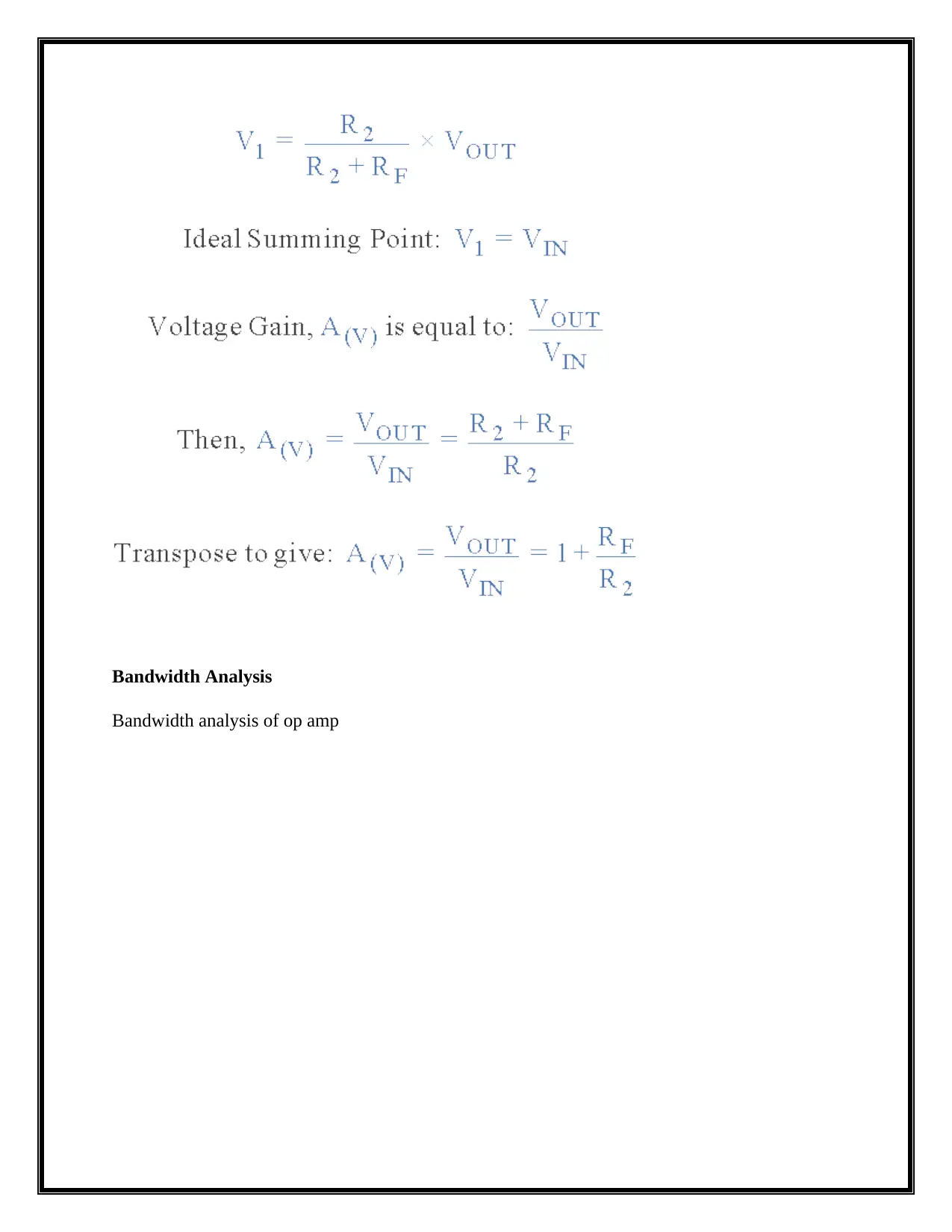
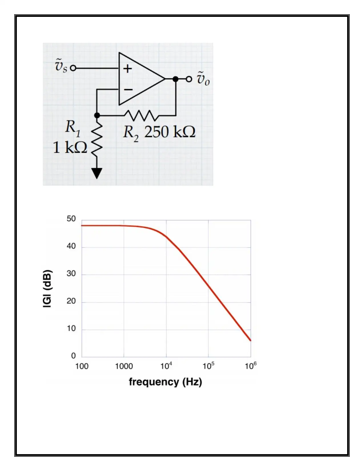
Homework Assignment
AI Summary
This assignment delves into the analysis and design of operational amplifier (op-amp) circuits. It begins with an introduction to op-amps, including inverting and non-inverting configurations, and explores the concept of negative feedback for gain stabilization. The assignment then proceeds to analyze open-loop frequency response, calculating phase margin and crossover frequency. Closed-loop analysis is performed, with the determination of closed-loop gain and consideration of stability characteristics. The concept of dominant pole compensation is introduced as a method to improve stability and bandwidth. The assignment also explores Miller compensation techniques, determining compensation capacitor values and implementing compensation to measure the compensated crossover frequency and phase margin. Further, the document covers frequency response analysis using Bode plots and calculates closed-loop gain and bandwidth. Finally, the assignment verifies closed-loop amplifier stability and provides relevant references.

1 out of 17
Related Documents


Your All-in-One AI-Powered Toolkit for Academic Success.
+13062052269
info@desklib.com
Available 24*7 on WhatsApp / Email
![[object Object]](/_next/static/media/star-bottom.7253800d.svg)
Copyright © 2020–2026 A2Z Services. All Rights Reserved. Developed and managed by ZUCOL.