Embedded System Design: Microcontroller Comparison and Analysis
VerifiedAdded on  2021/04/24
|28
|5205
|21
Report
AI Summary
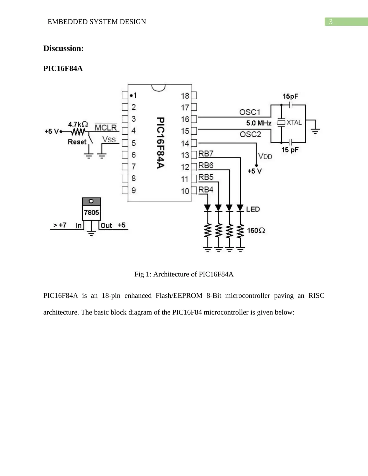
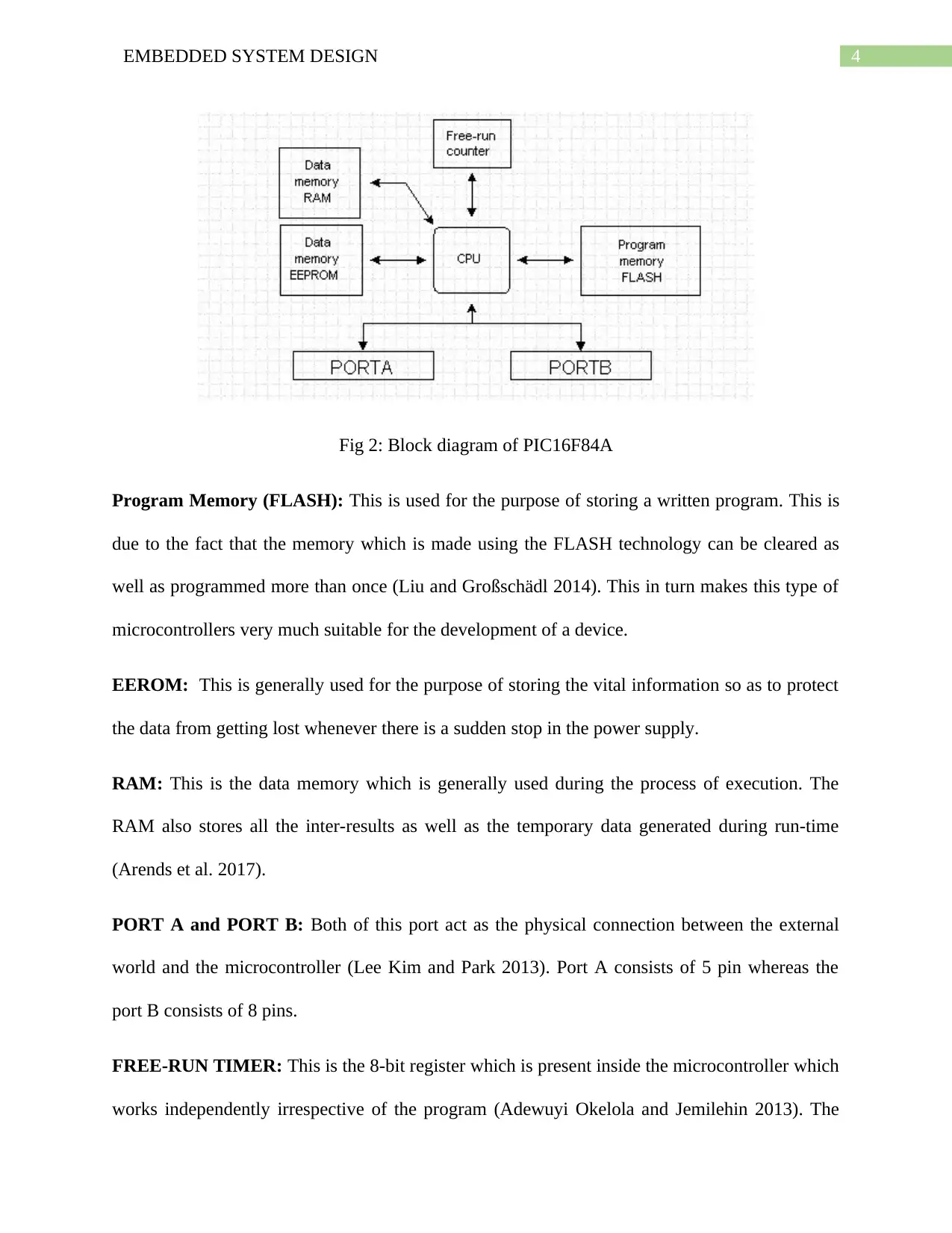
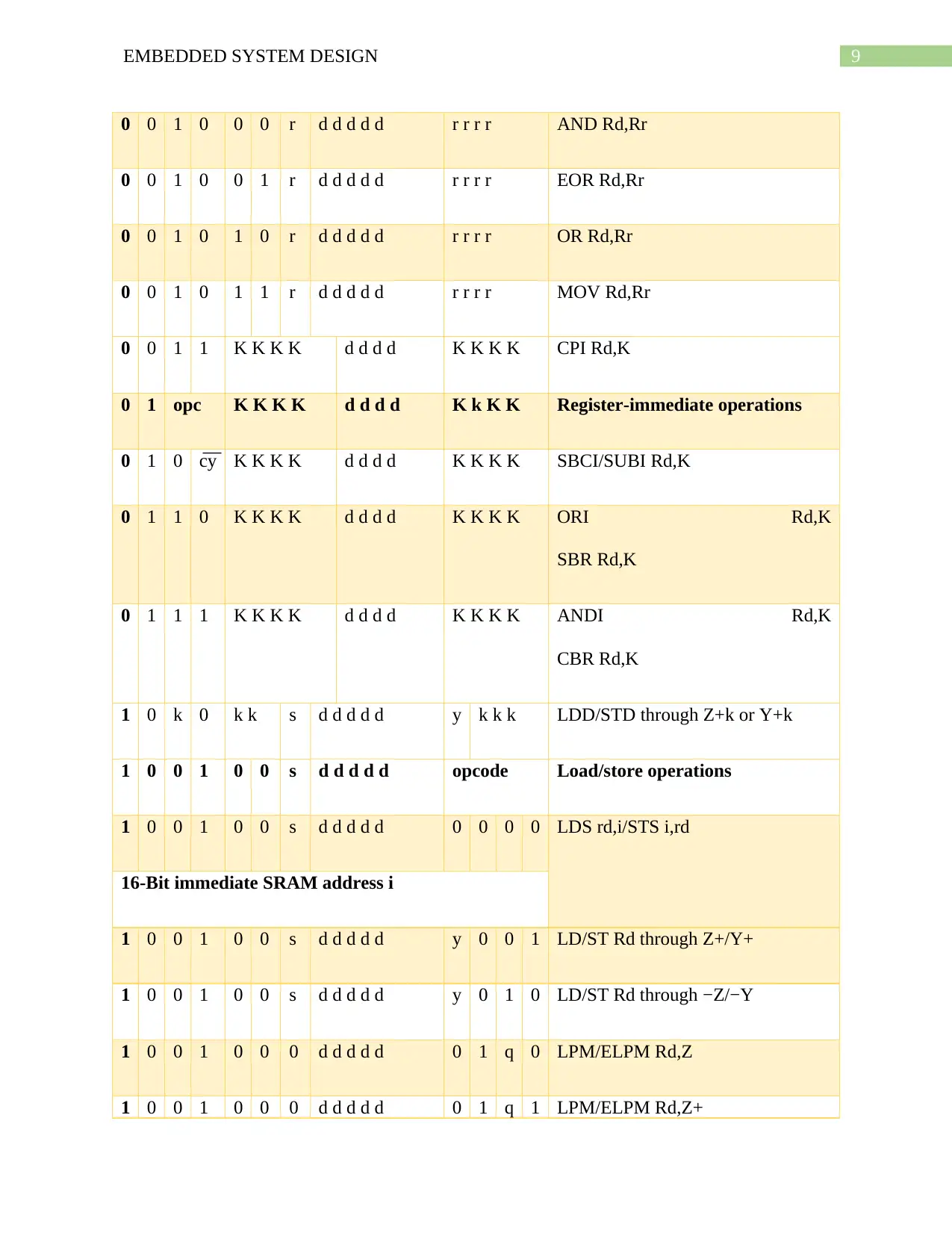
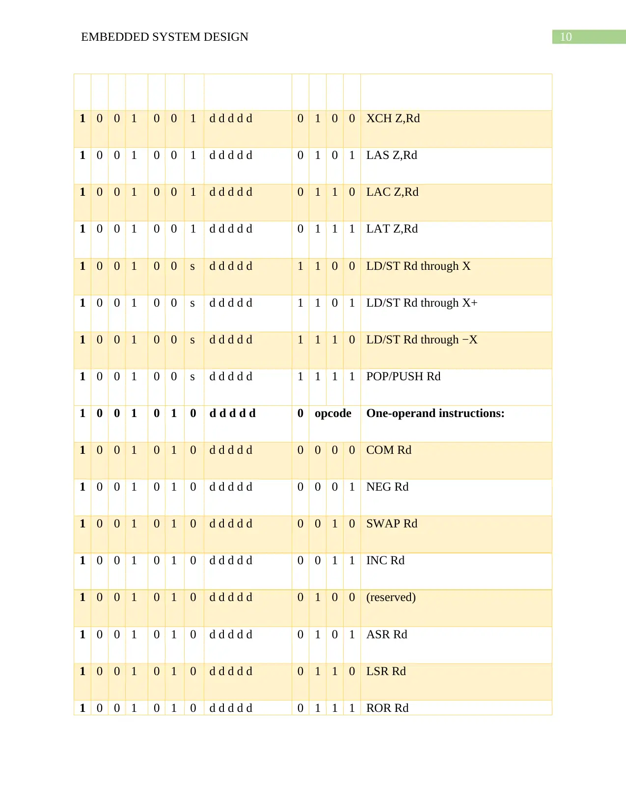
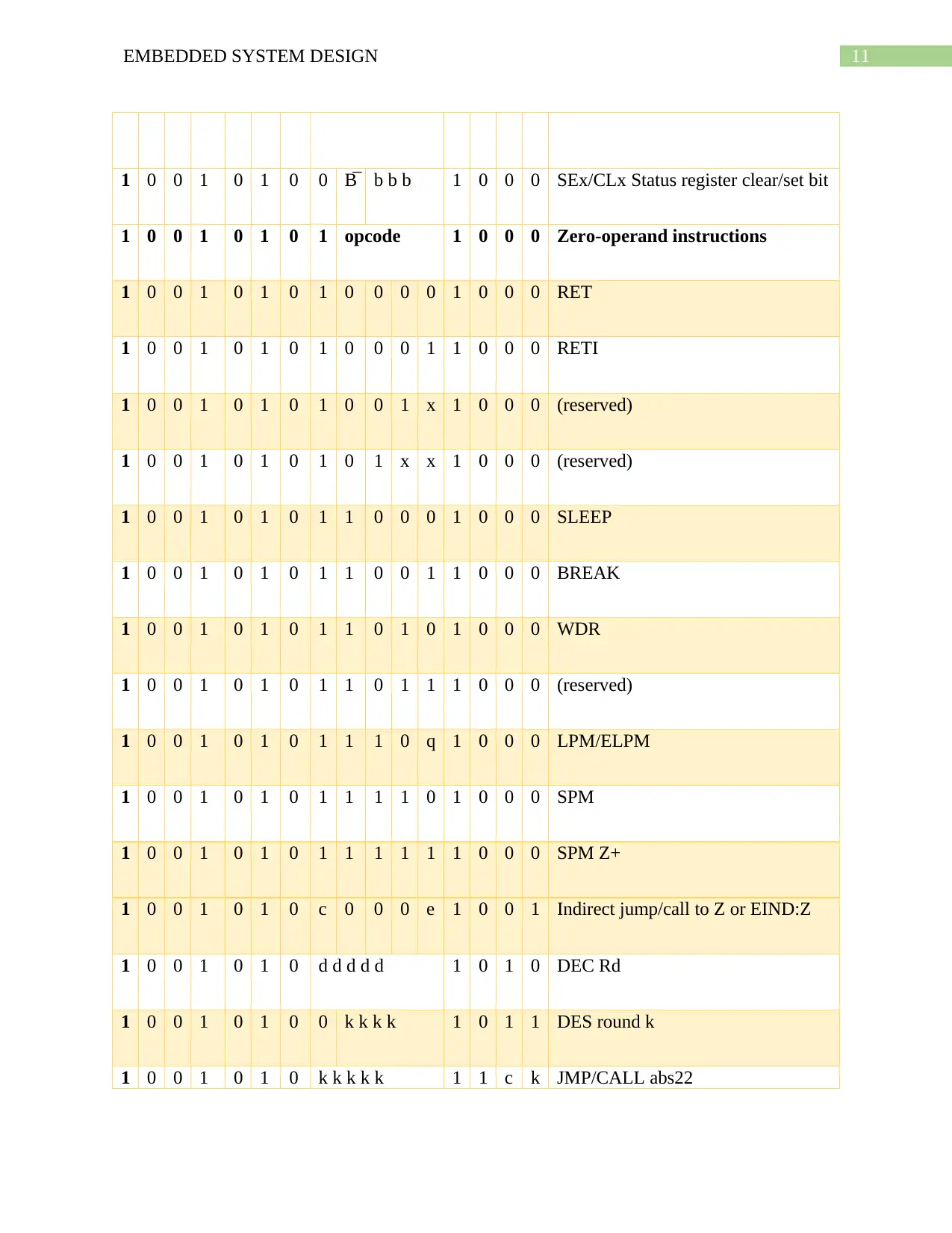
This report provides a comparative analysis of three microcontrollers: PIC16F84A, ATMEGA328P, and ATMEL89C51, crucial components in embedded system design. The report delves into each microcontroller's architecture, detailing components like CPU, memory (Flash, EEPROM, RAM), and input/output ports. It explores the instruction sets of each, providing mnemonics and descriptions for PIC16F84A and an overview of the ATMEGA328P and ATMEL89C51 instructions. Pin diagrams are presented to illustrate the physical connections and functionalities of each microcontroller. The discussion encompasses memory organization, peripherals, speed, cost, development tools, and potential applications of each microcontroller. The report concludes with a summary of the comparisons, highlighting strengths and weaknesses to aid in informed decision-making for embedded system projects. References are provided for further study and research.

Running head: EMBEDDED SYSTEM DESIGN
Embedded System Design
[Name of the Student]
[Name of the University]
[Author note]
Embedded System Design
[Name of the Student]
[Name of the University]
[Author note]
Paraphrase This Document
Need a fresh take? Get an instant paraphrase of this document with our AI Paraphraser

1EMBEDDED SYSTEM DESIGN
Table of Contents
Introduction:....................................................................................................................................2
Discussion:.......................................................................................................................................3
PIC16F84A..................................................................................................................................3
Instruction set of PIC16F84A:.................................................................................................5
Pin diagram of PIC16F84A:....................................................................................................6
ATMEGA328P............................................................................................................................7
Instruction set of ATMEGA328P overview:...........................................................................8
BIT assignments of ATMEGA328P......................................................................................12
Pin diagram of ATMEGA328P:............................................................................................14
ATMEL89C51...........................................................................................................................15
Block diagram of ATMEL 89C51.........................................................................................17
Pin diagram of ATMEL89C51:.............................................................................................19
Instruction set of ATMEL 89C51:.........................................................................................19
Summary of comparison:...............................................................................................................26
Conclusion:....................................................................................................................................27
References:....................................................................................................................................29

2EMBEDDED SYSTEM DESIGN
Introduction:
Microcontroller or MCU generally refers to the small computer that present on a small
integrated circuit. According to the modern terminology it can be stated that MCU is almost
similar to a system on a chip but it is less sophisticated (Mouha et al. 2014). MCU can be one of
the components of SoC or System on a Chip. A MCU is divided in several parts and this might
include one or more CPUs, associated with a memory and peripherals for input and output. MCU
are generally designed for the embedded applications in contrast to the microprocessors that are
used in the personal computers and any other general purpose applications which consists of the
various discrete chips (Pöppelmann Oder and Güneysu 2015). This report generally compares
the three microcontroller with respect to their Architecture, Instruction sets, Families, Memory,
Peripherals, Speed, Cost, Development tools and Applications.
⊘ This is a preview!⊘
Do you want full access?
Subscribe today to unlock all pages.

Trusted by 1+ million students worldwide

3EMBEDDED SYSTEM DESIGN
Discussion:
PIC16F84A
Fig 1: Architecture of PIC16F84A
PIC16F84A is an 18-pin enhanced Flash/EEPROM 8-Bit microcontroller paving an RISC
architecture. The basic block diagram of the PIC16F84 microcontroller is given below:
Discussion:
PIC16F84A
Fig 1: Architecture of PIC16F84A
PIC16F84A is an 18-pin enhanced Flash/EEPROM 8-Bit microcontroller paving an RISC
architecture. The basic block diagram of the PIC16F84 microcontroller is given below:
Paraphrase This Document
Need a fresh take? Get an instant paraphrase of this document with our AI Paraphraser

4EMBEDDED SYSTEM DESIGN
Fig 2: Block diagram of PIC16F84A
Program Memory (FLASH): This is used for the purpose of storing a written program. This is
due to the fact that the memory which is made using the FLASH technology can be cleared as
well as programmed more than once (Liu and Großschädl 2014). This in turn makes this type of
microcontrollers very much suitable for the development of a device.
EEROM: This is generally used for the purpose of storing the vital information so as to protect
the data from getting lost whenever there is a sudden stop in the power supply.
RAM: This is the data memory which is generally used during the process of execution. The
RAM also stores all the inter-results as well as the temporary data generated during run-time
(Arends et al. 2017).
PORT A and PORT B: Both of this port act as the physical connection between the external
world and the microcontroller (Lee Kim and Park 2013). Port A consists of 5 pin whereas the
port B consists of 8 pins.
FREE-RUN TIMER: This is the 8-bit register which is present inside the microcontroller which
works independently irrespective of the program (Adewuyi Okelola and Jemilehin 2013). The

5EMBEDDED SYSTEM DESIGN
value gets incremented after each fourth clock of the oscillator and continue to get incremented
unless and until the maximum value is reached i.e. 255. After reaching the maximum value it
again starts from Zero.
CENTRAL PROCESSING UNIT: This is responsible for connecting the different elements
present at the other blocks of the microcontroller (Bates 2013). It is responsible for coordinating
the works of the different blocks along with executing the user programs.
Instruction set of PIC16F84A:
Mnemonics & Operands Description
ADDWF f,d Add contents of W-register and f and store the contents in the
specified address(d)
ANDWF f,d AND the contents of W-register and f and store the contents in
the specified address(d)
CLRF f Clear the contents of f
CLRW Clear the contents of W-register
COMF f,d Compliments the contents of f and stores the result in
d(destination)
DECF f,d Decrement f and store the result in the destination(d)
DECFSZ f,d Decrement f, skip if zero
INCF f,d Increment f and store the result in destination (d)
INCFSZ f,d Increment f, skip if zero
IORWF f,d Incluse OR contents of W-register with contents of f and store
the result in destination(d)
MOVF f,d move the contents of f to destination(d)
MOVWF f Move the contents of W-register to fM
NOP No operation (remains quiet for one cycle)
RLF f,d Rotate left f through carry
RRF f,d Rotate right f through carry
SUBWF f,d Subtract contents of W-register from f
⊘ This is a preview!⊘
Do you want full access?
Subscribe today to unlock all pages.

Trusted by 1+ million students worldwide

6EMBEDDED SYSTEM DESIGN
SWAPF f,d Swaps nibbles in f
XORWF f,d Exclusive OR contents of W-register with f
Pin diagram of PIC16F84A:
SWAPF f,d Swaps nibbles in f
XORWF f,d Exclusive OR contents of W-register with f
Pin diagram of PIC16F84A:
Paraphrase This Document
Need a fresh take? Get an instant paraphrase of this document with our AI Paraphraser

7EMBEDDED SYSTEM DESIGN
ATMEGA328P
Fig 3: Architecture of ATMEGA328P
ATmega328P is a microchip having high performance along with a low power design.
This is a 32K 8-bit microcontroller which is based upon the AVR architecture. In a single clock
many of the instructions are executed which initially provides a throughput of around 20 MIPS at
a frequency of 20 MHz. This is an 8-bit microcontroller which is having an advanced RISC
architecture (Mellis et al. 2013). There are 131 instruction and most of this instructions are
executed in a single clock cycle and has a throughput of about 20 MIPS at 20 MHz. there are
32X8 registers in working state.
MEMORY: This microprocessor includes a 32 KB programmable FLASH, 1KB EPROM, and 2
KB SRAM. Along with this there is also 10,000 cycles for erase and write in FLASH and
100,000 cycle for the EEPROM. Along with this there is also an optional boot loader associated
with lock bits and a programming lock for the security of the software (Sarkar and Chowdhury
2015).

8EMBEDDED SYSTEM DESIGN
INPUT/OUTPUT PACKAGES: This microcontroller consists of 23 programmable
input/output lines and have a 28 pin PDIP package. This microcontroller operates at a voltage of
1.8-5.5 Volts and -400C to 850 C (Chang et al. 2013).
Instruction set of ATMEGA328P overview:
1
5
1
4
1
3
1
2
1
1
1
0 9 8 7 6 5 4 3 2 1 0
Instruction
0 0 0 0 0 0 0 0 0 0 0 0 0 0 0 0 NOP
0 0 0 0 0 0 0 1 D D D D R R R R MOVW Rd,Rr Move register pair
0 0 0 0 0 0 1 0 d d d d r r r r MULS Rd,Rr
0 0 0 0 0 0 1 1 0 d d d 0 r r r MULSU Rd,Rr
0 0 0 0 0 0 1 1 0 d d d 1 r r r FMUL Rd,Rr
0 0 0 0 0 0 1 1 1 d d d u r r r FMULS(U) Rd,Rr
0 0 opcode r d d d d d r r r r 2-operand instructions
0 0 0 cÌ…yÌ… 0 1 r d d d d d r r r r CPC/CP Rd,Rr
0 0 0 cÌ…yÌ… 1 0 r d d d d d r r r r SBC/SUB Rd,Rr
0 0 0 cy 1 r d d d d d d r r r r ADD/ADC Rd,Rr (LSL/ROL Rd
when Rd=Rr)
0 0 0 1 0 0 r d d d d d r r r r CPSE Rd,Rr
⊘ This is a preview!⊘
Do you want full access?
Subscribe today to unlock all pages.

Trusted by 1+ million students worldwide

9EMBEDDED SYSTEM DESIGN
0 0 1 0 0 0 r d d d d d r r r r AND Rd,Rr
0 0 1 0 0 1 r d d d d d r r r r EOR Rd,Rr
0 0 1 0 1 0 r d d d d d r r r r OR Rd,Rr
0 0 1 0 1 1 r d d d d d r r r r MOV Rd,Rr
0 0 1 1 K K K K d d d d K K K K CPI Rd,K
0 1 opc K K K K d d d d K k K K Register-immediate operations
0 1 0 cÌ…yÌ… K K K K d d d d K K K K SBCI/SUBI Rd,K
0 1 1 0 K K K K d d d d K K K K ORI Rd,K
SBR Rd,K
0 1 1 1 K K K K d d d d K K K K ANDI Rd,K
CBR Rd,K
1 0 k 0 k k s d d d d d y k k k LDD/STD through Z+k or Y+k
1 0 0 1 0 0 s d d d d d opcode Load/store operations
1 0 0 1 0 0 s d d d d d 0 0 0 0 LDS rd,i/STS i,rd
16-Bit immediate SRAM address i
1 0 0 1 0 0 s d d d d d y 0 0 1 LD/ST Rd through Z+/Y+
1 0 0 1 0 0 s d d d d d y 0 1 0 LD/ST Rd through −Z/−Y
1 0 0 1 0 0 0 d d d d d 0 1 q 0 LPM/ELPM Rd,Z
1 0 0 1 0 0 0 d d d d d 0 1 q 1 LPM/ELPM Rd,Z+
Paraphrase This Document
Need a fresh take? Get an instant paraphrase of this document with our AI Paraphraser

10EMBEDDED SYSTEM DESIGN
1 0 0 1 0 0 1 d d d d d 0 1 0 0 XCH Z,Rd
1 0 0 1 0 0 1 d d d d d 0 1 0 1 LAS Z,Rd
1 0 0 1 0 0 1 d d d d d 0 1 1 0 LAC Z,Rd
1 0 0 1 0 0 1 d d d d d 0 1 1 1 LAT Z,Rd
1 0 0 1 0 0 s d d d d d 1 1 0 0 LD/ST Rd through X
1 0 0 1 0 0 s d d d d d 1 1 0 1 LD/ST Rd through X+
1 0 0 1 0 0 s d d d d d 1 1 1 0 LD/ST Rd through −X
1 0 0 1 0 0 s d d d d d 1 1 1 1 POP/PUSH Rd
1 0 0 1 0 1 0 d d d d d 0 opcode One-operand instructions:
1 0 0 1 0 1 0 d d d d d 0 0 0 0 COM Rd
1 0 0 1 0 1 0 d d d d d 0 0 0 1 NEG Rd
1 0 0 1 0 1 0 d d d d d 0 0 1 0 SWAP Rd
1 0 0 1 0 1 0 d d d d d 0 0 1 1 INC Rd
1 0 0 1 0 1 0 d d d d d 0 1 0 0 (reserved)
1 0 0 1 0 1 0 d d d d d 0 1 0 1 ASR Rd
1 0 0 1 0 1 0 d d d d d 0 1 1 0 LSR Rd
1 0 0 1 0 1 0 d d d d d 0 1 1 1 ROR Rd

11EMBEDDED SYSTEM DESIGN
1 0 0 1 0 1 0 0 BÌ… b b b 1 0 0 0 SEx/CLx Status register clear/set bit
1 0 0 1 0 1 0 1 opcode 1 0 0 0 Zero-operand instructions
1 0 0 1 0 1 0 1 0 0 0 0 1 0 0 0 RET
1 0 0 1 0 1 0 1 0 0 0 1 1 0 0 0 RETI
1 0 0 1 0 1 0 1 0 0 1 x 1 0 0 0 (reserved)
1 0 0 1 0 1 0 1 0 1 x x 1 0 0 0 (reserved)
1 0 0 1 0 1 0 1 1 0 0 0 1 0 0 0 SLEEP
1 0 0 1 0 1 0 1 1 0 0 1 1 0 0 0 BREAK
1 0 0 1 0 1 0 1 1 0 1 0 1 0 0 0 WDR
1 0 0 1 0 1 0 1 1 0 1 1 1 0 0 0 (reserved)
1 0 0 1 0 1 0 1 1 1 0 q 1 0 0 0 LPM/ELPM
1 0 0 1 0 1 0 1 1 1 1 0 1 0 0 0 SPM
1 0 0 1 0 1 0 1 1 1 1 1 1 0 0 0 SPM Z+
1 0 0 1 0 1 0 c 0 0 0 e 1 0 0 1 Indirect jump/call to Z or EIND:Z
1 0 0 1 0 1 0 d d d d d 1 0 1 0 DEC Rd
1 0 0 1 0 1 0 0 k k k k 1 0 1 1 DES round k
1 0 0 1 0 1 0 k k k k k 1 1 c k JMP/CALL abs22
⊘ This is a preview!⊘
Do you want full access?
Subscribe today to unlock all pages.

Trusted by 1+ million students worldwide
1 out of 28
Related Documents

Your All-in-One AI-Powered Toolkit for Academic Success.
 +13062052269
info@desklib.com
Available 24*7 on WhatsApp / Email
Unlock your academic potential
Copyright © 2020–2025 A2Z Services. All Rights Reserved. Developed and managed by ZUCOL.