Engineering Design: PCB Design, Stakeholders, and Planning Techniques
VerifiedAdded on 2021/01/01
|9
|1982
|192
Report
AI Summary
This report delves into the intricacies of printed circuit board (PCB) design, starting with an overview of PCB characteristics, including the significance of material selection, through-hole vs. surface mount technology (SMT), and trace design. It then examines the impact of stakeholders, such as clients, design engineers, and manufacturers, on design specifications. The report emphasizes the role of critical path analysis (CPA) in project management for timely execution and identifies different planning techniques like action, strategic, operational, tactical, and contingency planning, highlighting their applications in the context of PCB design and manufacturing. The report also discusses inspection techniques, including board-level testing, circuit-level testing, and the use of Automated Test Equipment (ATE) and In-Circuit Testing (ICT) to ensure design accuracy and cost-effectiveness. It concludes by emphasizing the importance of selecting appropriate planning methods to enhance operational efficiency and address challenges in PCB manufacturing. The report is supported by references to books, journals, and online resources.
ENGINEERING DESIGN
Paraphrase This Document
Need a fresh take? Get an instant paraphrase of this document with our AI Paraphraser
TABLE OF CONTENTS
PART 1: Design specification preparation .....................................................................................1
Characteristics of printed circuit board (PCB) and current techniques for inspection ...............1
Impact of stakeholders on design brief ......................................................................................2
Critical path analysis (CPA) in project management .................................................................2
Potential planning techniques ....................................................................................................3
REFERENCES ...............................................................................................................................6
PART 1: Design specification preparation
Characteristics of printed circuit board (PCB) and current techniques for inspection
PCB provides mechanical support and electrical connection path for electrical and
electronic components. The errors in PCB designing can affect the functioning of device. Thus,
various factors such as size, connections, width and material used plays significant role in
influencing the overall performance. The suitable base material selection avoids delamination
and other technical errors such as open circuit (Top 10 characteristics of highly reliable PCB).
For designing purpose various through hole or surface mounted technology can be used.
In through hole method holes are used to insert the leads and other soldering is used on
other side of board. However, the need of extremely precise holes can increase cost as well as
limitations for routing area in multi layered PCB. Thus instead of this method surface mounted
technique is preferred for PCB design. In surface mounting instead of using holes components
are redesigned with metallic caps so that they can be soldered directly on circuit board. Surface
mounting technology (SMD) has higher component density. The trace thickness and width
affects the resistance and conducting current.
Design specification and testing: The PCB is fabricated by using materials like laminates,
copper foil, copper clad laminates and resin. The conducting path or traces on PCB are residuals
of etching process. The substrate used in the designing process is dielectric material and consist
of epoxy resin and glass fibre or woven as a reinforcement (Harrison and Lock, 2017). In order
to make designing process cost effective and simple PCB is tested and inspected at various
levels. The modern test jigs are also provided with electronic intelligence so that tools can
operate in all directions. Along with the jigs automated test equipments (ATE) can also identify
PCB and are applicable at on chip level as well as integrated circuit The inspection can use
following techniques:
Board level testing: With this approach circuit defined by the netlist is tested on fabricated PCB.
It also includes the open and short circuit test analysis. When the board is verified then it is also
required for the designers to perform ATE. Though it is expensive but is essential to analyse the
designing defects in functionality.
Circuit level: One of the most advance and widely use ATE test is in-circuit test (ICT) to check
the connections, functionality and value of components mounted on PCB. The JTAG boundary
1
⊘ This is a preview!⊘
Do you want full access?
Subscribe today to unlock all pages.
Trusted by 1+ million students worldwide
scanning use test logics to evaluate the accuracy of soldering and component insertion into PCB.
In the circuit level verification functional testers can be used in which board is simulated with the
external parameters. These type of verification makes the designing process more reliable and
enables to identify defects at the initial stages of designing so that cost, time and resources can be
saved.
Impact of stakeholders on design brief
The designing perspective and efficiency greatly depends upon the different stakeholders
who are associated with the PCB design. The designing constraints such as material used,
technology and testing approaches are influenced by the stakeholders. The PCB must be
designed as per the requirement of device or the application for which it is being designed. The
resistance and capacitance of the track on PCB affects the performance (Vanichchinchai and
Duantrakoonsil, 2018). These attributes thus play significant role in radio frequency applications
and transmissions related applications. Hence, the circuit design and material selected for the
conducting and dielectric functionality greatly depends upon the needs of clients.
Apart from the clients different stakeholders such as designing and testing engineers,
manufacturers are also an integral part for changing the design characteristics of PCB. The
project engineers determine that the available resources must be in alignment with the design
technology so that design can be completed on time and within prescribed budget frames. The
layout of the design is prepared in a way that it must be feasible for the mechanical engineers to
implement it practically without bringing any functional complications. With the rapidly
advancing technology the manufacturers are required to design the circuit boards on which
greater number of components can be mounted so that cost can be reduced.
However, the assembly engineers cannot simply increase the component density and thus
they must interact and plan with the design specification and testing engineers (Rybakov and
et.al., 2017). The vendors which supply the material for PCB fabrication must also be
communicated regularly so that the raw material is available for the manufacturing process.
Critical path analysis (CPA) in project management
The critical path analysis is an essential strategy to accomplish the project task on time.
The CPA will help to execute essential activities of PCB fabrication on time with proper
scheduling and by identifying the interrelations between various activities. This approach help to
2
Paraphrase This Document
Need a fresh take? Get an instant paraphrase of this document with our AI Paraphraser
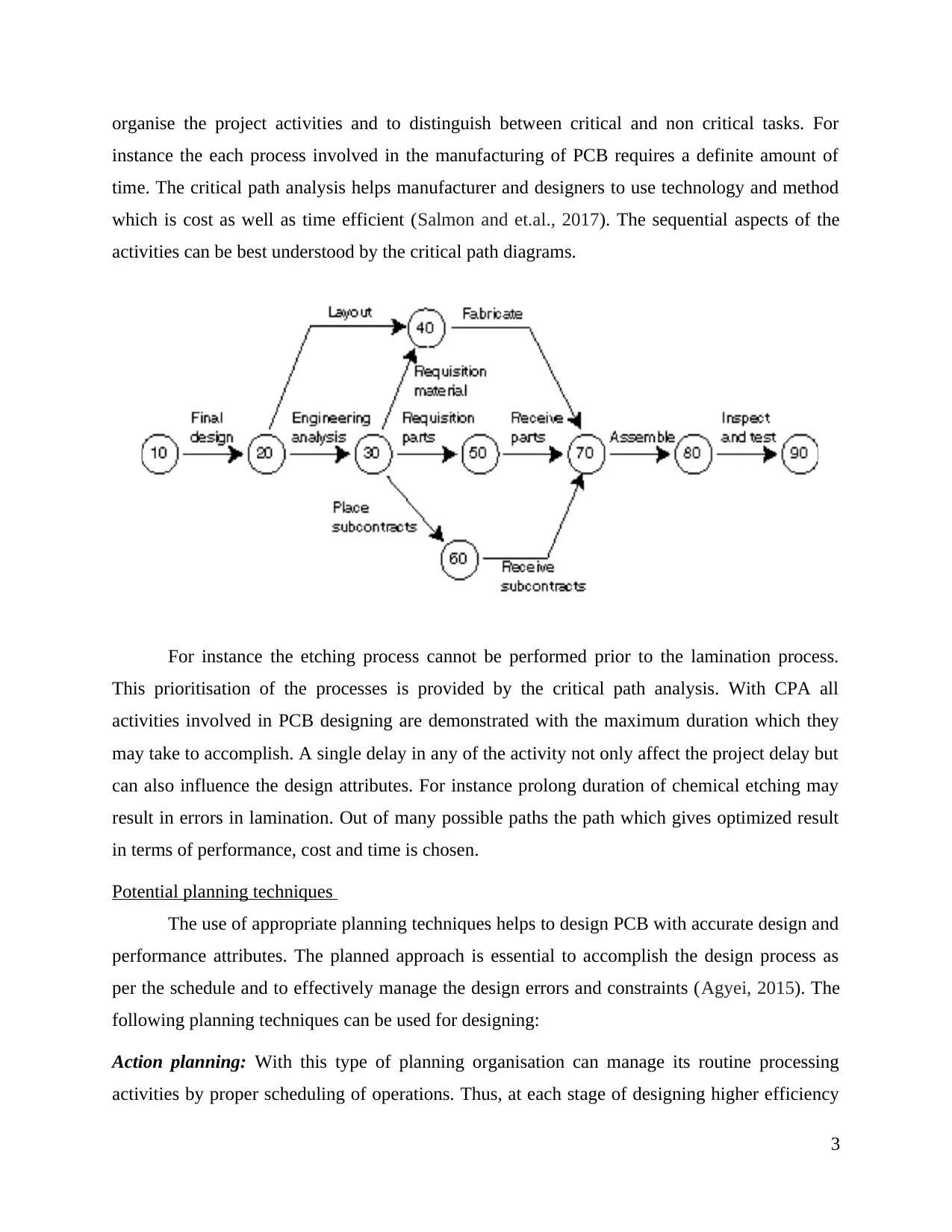
organise the project activities and to distinguish between critical and non critical tasks. For
instance the each process involved in the manufacturing of PCB requires a definite amount of
time. The critical path analysis helps manufacturer and designers to use technology and method
which is cost as well as time efficient (Salmon and et.al., 2017). The sequential aspects of the
activities can be best understood by the critical path diagrams.
For instance the etching process cannot be performed prior to the lamination process.
This prioritisation of the processes is provided by the critical path analysis. With CPA all
activities involved in PCB designing are demonstrated with the maximum duration which they
may take to accomplish. A single delay in any of the activity not only affect the project delay but
can also influence the design attributes. For instance prolong duration of chemical etching may
result in errors in lamination. Out of many possible paths the path which gives optimized result
in terms of performance, cost and time is chosen.
Potential planning techniques
The use of appropriate planning techniques helps to design PCB with accurate design and
performance attributes. The planned approach is essential to accomplish the design process as
per the schedule and to effectively manage the design errors and constraints (Agyei, 2015). The
following planning techniques can be used for designing:
Action planning: With this type of planning organisation can manage its routine processing
activities by proper scheduling of operations. Thus, at each stage of designing higher efficiency
3
and accuracy can be achieved. The quality and attributes of resources can also be controlled and
monitored after execution of each task. For the PCB manufacturing company this type of
planning is effective because it will help to bring accuracy at each stage and thus cost and quality
will be sustained (Vanichchinchai and Duantrakoonsil, 2018).
Strategic planning: With this planning approach various stakeholders work together to achieve a
common goal. The execution strategies are developed according to the long term goals of
company. However, this type of planning technique will not be suitable for the PCB
manufacturing company because since all designing process is carried out by various teams, they
are already integrated with each other. Thus, there needs a better planning which enhances the
efficiency.
Operational planning: The operational approach of planning integrates different functions with
long term business objectives of the company (Harrison and Lock, 2017). It can also be used for
the given case study because the operational efficiency will naturally improve the design
requirements and overall performance. Operational planning helps to improve various aspects of
resources, funds and design requirements of PCB.
Tactical planning: On the basis of strategic plan different activities are divided into short term
activities so that every stage can be completed with better focus. It also helps different team
members to have clarity of their roles and requirements because instead of focusing on different
operations individual team members focus on their particular task.
Contingency planning technique: Contingency technique analyse the risks which can influence
the overall implementation of the project. Thus, its main aspect is to evaluate the future risks
which may be difficult to neglect and thus require planning to survive. This cannot be considered
as the suitable planning technique for the manufacturing company because instead of accomplish
task its key focus is to sustain in situations of unpredictable risks.
Assumption based technique: This planning technique is based upon assuming the future
considerations which may influence the process and benefits. Though this planning technique is
not suitable for the current requirements of the company but is essential to employ this for future
reference (Kerzner and Kerzner, 2017). For instance the number of components which are
mounted on PCB are getting enhanced day by day thus company must have proper planning that
how it will cope up with these future advancements in terms of cost and available resources.
4
⊘ This is a preview!⊘
Do you want full access?
Subscribe today to unlock all pages.
Trusted by 1+ million students worldwide

Thus, PCB manufacturer must choose their planning method with due care so that operational
efficiency can be increased. It will also help to adopt a systematic method to overcome
challenges which prevents the growth of business and to integrate different functional units of
organisation (Vanichchinchai and Duantrakoonsil, 2018). For the company operational or action
planning technique will be highly suitable to achieve the desired monitoring and accuracy in the
manufacturing process.
5
Paraphrase This Document
Need a fresh take? Get an instant paraphrase of this document with our AI Paraphraser
REFERENCES
Books and Journals
Agyei, W., 2015. Project planning and scheduling using PERT and CPM techniques with linear
programming: case study.International Journal of Scientific & Technology
Research.4(8). pp.222-227.
Harrison, F. and Lock, D., 2017. Advanced project management: a structured approach.
Routledge.
Kerzner, H. and Kerzner, H.R., 2017. Project management: a systems approach to planning,
scheduling, and controlling. John Wiley & Sons.
MacCrimmon, K.R., 2016. Critical path analysis. The New Palgrave Dictionary of Economics,
pp.1-3.
Rybakov, I.M., and et.al., 2017, January. Application of the model of the printed circuit board
with regard to the topology of external conductive layers for calculation of the thermal
conditions of the printed circuit board. In Journal of Physics: Conference Series (Vol.
803, No. 1, p. 012130). IOP Publishing.
Salmon, P.M., and et.al., 2017. Critical Path Analysis: Ladbroke Grove Case Study. In Human
Factors Methods and Accident Analysis (pp. 165-172). CRC Press.
Vanichchinchai, A. and Duantrakoonsil, W., 2018. Quality improvement of printed circuit board:
A case study of copper in hole. Science, Engineering and Health Studies (FORMER
NAME" SILPAKORN UNIVERSITY SCIENCE AND TECHNOLOGY
JOURNAL"). 12(2). pp.77-84.
Online
Top 10 characteristics of highly reliable PCB, 2015 [Online] Accessed through
<http://www.dnatechindia.com/top-characteristics-of-good-quality-printed-circuit-board-
pcb.html>
6

7
⊘ This is a preview!⊘
Do you want full access?
Subscribe today to unlock all pages.
Trusted by 1+ million students worldwide
1 out of 9


Your All-in-One AI-Powered Toolkit for Academic Success.
+13062052269
info@desklib.com
Available 24*7 on WhatsApp / Email
![[object Object]](/_next/static/media/star-bottom.7253800d.svg)
Unlock your academic potential
Copyright © 2020–2026 A2Z Services. All Rights Reserved. Developed and managed by ZUCOL.