Electrical Engineering: 4305ELE/4608IYO - Timer Design and Testing
VerifiedAdded on 2023/04/21
|12
|3964
|460
Practical Assignment
AI Summary
This document presents a student's project on timer design as part of an Electrical Engineering Practice course (4305ELE/4608IYO). The project includes project management skills, amplifier design and testing, oscillator design and testing, and a delay unit. The amplifier section details the components used, experimental procedures, and observations, focusing on the effects of input frequency and resistor values. The oscillator section covers building an oscillator based on a NOR gate, evaluating its performance, and exploring the relationship between sound and frequency. The report also includes a 555 timer design, duty cycle effects, and concludes with veriboard design and packaging considerations. The student has provided a comprehensive overview of the design and testing process, including equipment used, experimental methods, and results obtained.
Abstract
An amplifier is used for signal amplitude increase from small level to high level that can be
useful to the owner. While raising the amplification of the signal from small levels to high the
signal details as well as the characteristics are constantly kept. The process is called linearly. The
greater linear can give more signal output. There are many kinds of amplifiers. In the field of
electronics, amplifiers are very significant in power, signal processing, amplification and many
other technological applications
Keywords: Project Management, Amplifiers, Circuit Design, 555 Timers, Veriboard design
Introduction
An amplifier is just an active electronic
device which can increase power of the
signal which can be either a time-varying
current or voltage. It actually works in the
two-port circuit of electronic nature which
uses electrical power from the power supply
to raise the amplitude of applied signal to its
terminals input, by producing proportional
greater output signal amplitude.[1] The
amplification quantity is given by amplifier
is measured through its gain: ratio of
current, power to input or to voltage. There
are kinds of amplifiers: Class A, B, AB, D,
G, D and H
1. Inquiry Questions to ABC
about the Quotation.
i. What type of timer do you want?
ii. Is it analog or digital display timer?
iii. Which type timing reliability do you
want?
iv. Is waterproof or loudest buzzer or
rugged?
v. What type of control mode do you
need?
vi. What operation model do you need?
vii. What is the input and output power
range?
viii. Do your workers need the training
for operating the timers?
ix. Do you need software updates?
x. Do you want it to be automated with
the SCADA or PLC?
xi. How many pieces of timers do you
need?
xii. Can installation cost be included?
2. Customer Feedback: The
specifications of the timers.
i. Both Digital timer and analog timers
ii. Timer with features such as
waterproof, intuitive and simple,
rugged and loudest buzzer.
iii. Low power input of 9V battery
iv. Output power of 9VDC that can be
built into power data loggers and
autodials
v. With different models for battery
powered with buttons outside and
inside to set timing cycle. It can be
also ac powered with relay control.
vi. With battery lifespan of six years at
least.
vii. Easily automated with the PLC and
SCADA.
viii. We need orientation and training of
your devices on how to use and
repair them.
ix. Software can be updated easily with
our experts.
x. About 30 pieces of the timer.
Paraphrase This Document
Need a fresh take? Get an instant paraphrase of this document with our AI Paraphraser
xi. Price quotation from you.
Features of the timers:
Easily adjustable from 1 second to
99 minutes with wide time range.
Easily installable
For Dc powered are low powered
Corrosion proof and water proof
It can count extra after it reaches
zero
Loud sound buzzers with maximum
of 103dB
It easy to operate it.
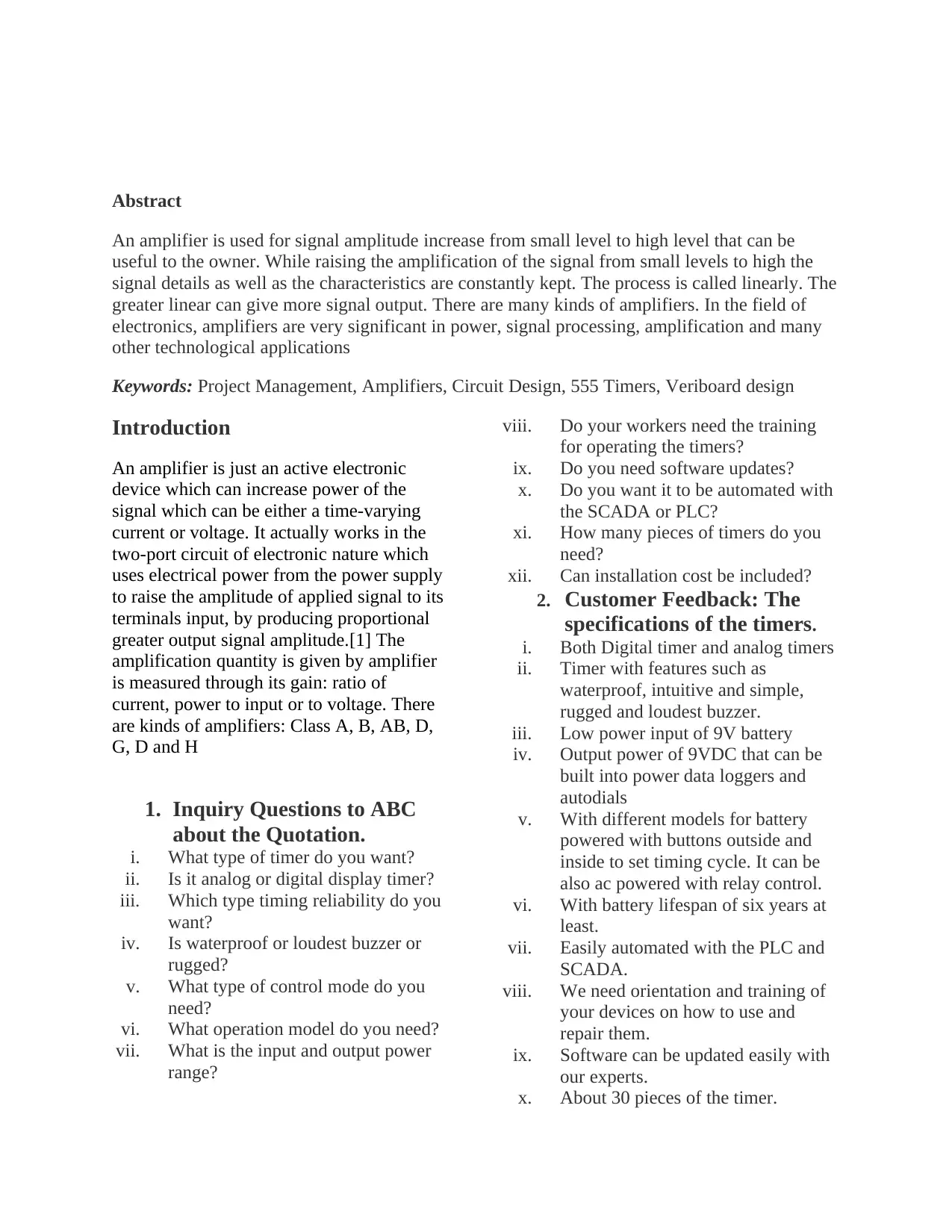
3. Timer Circuit developed
Figure 1: time circuit designed
Parameters Values Units
Dc output
voltage
5 V
Input Dc
voltage
9 V
Ac Output
Voltage
120 V
Ac Input
voltage
230 V
Battery
lifespan
6 Years
Display size 18 mm
Compact
size
100x100x50 mm
Loudest
Buzzer
103 dB
Ac in put
current
15 A
Ac output
current
15 A
Figure2
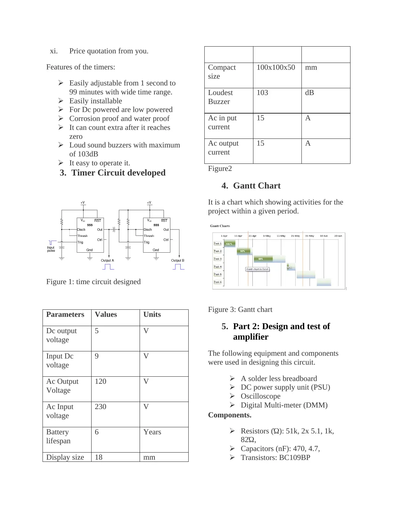
4. Gantt Chart
It is a chart which showing activities for the
project within a given period.
Figure 3: Gantt chart
5. Part 2: Design and test of
amplifier
The following equipment and components
were used in designing this circuit.
A solder less breadboard
DC power supply unit (PSU)
Oscilloscope
Digital Multi-meter (DMM)
Components.
Resistors (Ώ): 51k, 2x 5.1, 1k,
82Ώ,
Capacitors (nF): 470, 4.7,
Transistors: BC109BP
Features of the timers:
Easily adjustable from 1 second to
99 minutes with wide time range.
Easily installable
For Dc powered are low powered
Corrosion proof and water proof
It can count extra after it reaches
zero
Loud sound buzzers with maximum
of 103dB
It easy to operate it.
3. Timer Circuit developed
Figure 1: time circuit designed
Parameters Values Units
Dc output
voltage
5 V
Input Dc
voltage
9 V
Ac Output
Voltage
120 V
Ac Input
voltage
230 V
Battery
lifespan
6 Years
Display size 18 mm
Compact
size
100x100x50 mm
Loudest
Buzzer
103 dB
Ac in put
current
15 A
Ac output
current
15 A
Figure2
4. Gantt Chart
It is a chart which showing activities for the
project within a given period.
Figure 3: Gantt chart
5. Part 2: Design and test of
amplifier
The following equipment and components
were used in designing this circuit.
A solder less breadboard
DC power supply unit (PSU)
Oscilloscope
Digital Multi-meter (DMM)
Components.
Resistors (Ώ): 51k, 2x 5.1, 1k,
82Ώ,
Capacitors (nF): 470, 4.7,
Transistors: BC109BP
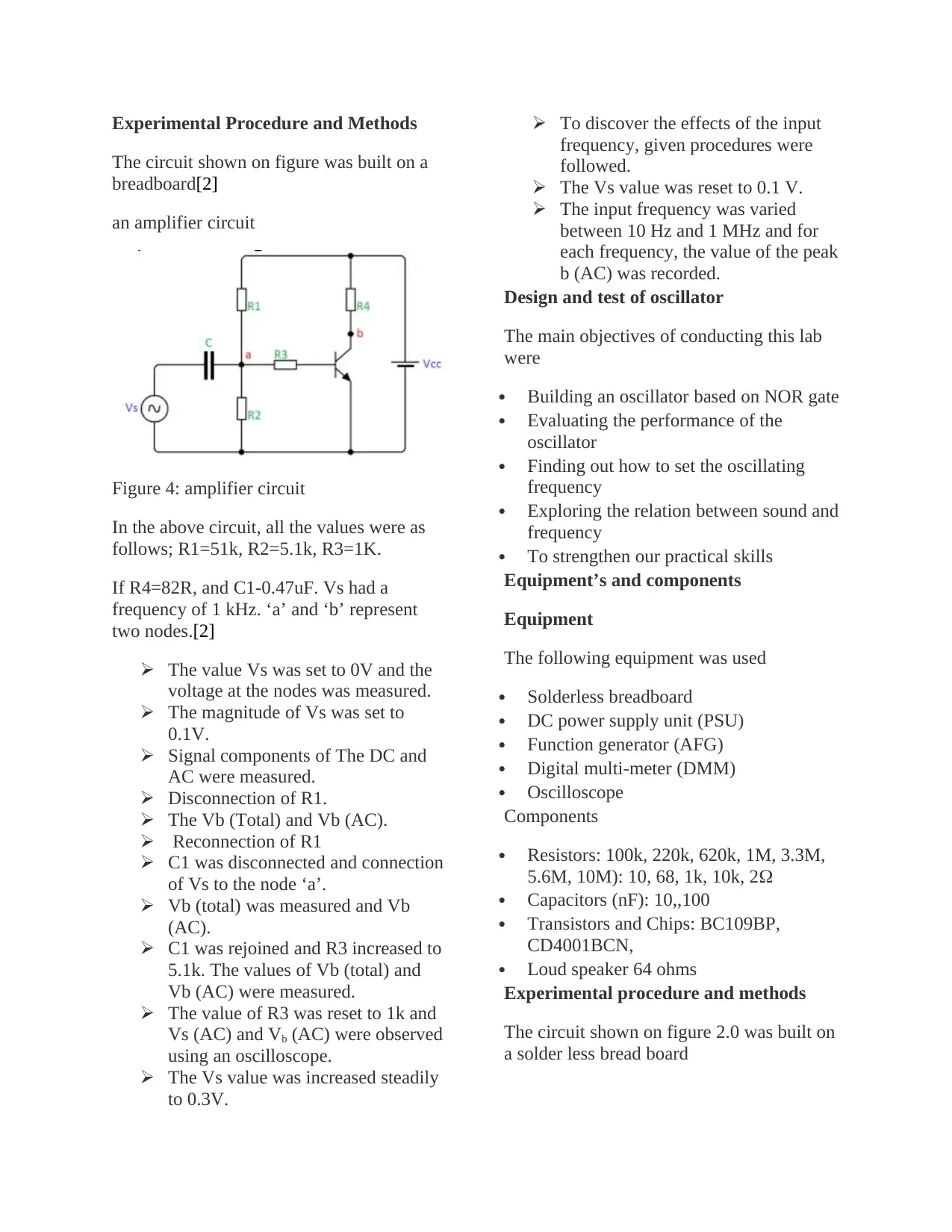
Experimental Procedure and Methods
The circuit shown on figure was built on a
breadboard[2]
an amplifier circuit
Figure 4: amplifier circuit
In the above circuit, all the values were as
follows; R1=51k, R2=5.1k, R3=1K.
If R4=82R, and C1-0.47uF. Vs had a
frequency of 1 kHz. ‘a’ and ‘b’ represent
two nodes.[2]
The value Vs was set to 0V and the
voltage at the nodes was measured.
The magnitude of Vs was set to
0.1V.
Signal components of The DC and
AC were measured.
Disconnection of R1.
The Vb (Total) and Vb (AC).
Reconnection of R1
C1 was disconnected and connection
of Vs to the node ‘a’.
Vb (total) was measured and Vb
(AC).
C1 was rejoined and R3 increased to
5.1k. The values of Vb (total) and
Vb (AC) were measured.
The value of R3 was reset to 1k and
Vs (AC) and Vb (AC) were observed
using an oscilloscope.
The Vs value was increased steadily
to 0.3V.
To discover the effects of the input
frequency, given procedures were
followed.
The Vs value was reset to 0.1 V.
The input frequency was varied
between 10 Hz and 1 MHz and for
each frequency, the value of the peak
b (AC) was recorded.
Design and test of oscillator
The main objectives of conducting this lab
were
Building an oscillator based on NOR gate
Evaluating the performance of the
oscillator
Finding out how to set the oscillating
frequency
Exploring the relation between sound and
frequency
To strengthen our practical skills
Equipment’s and components
Equipment
The following equipment was used
Solderless breadboard
DC power supply unit (PSU)
Function generator (AFG)
Digital multi-meter (DMM)
Oscilloscope
Components
Resistors: 100k, 220k, 620k, 1M, 3.3M,
5.6M, 10M): 10, 68, 1k, 10k, 2
Capacitors (nF): 10,,100
Transistors and Chips: BC109BP,
CD4001BCN,
Loud speaker 64 ohms
Experimental procedure and methods
The circuit shown on figure 2.0 was built on
a solder less bread board
⊘ This is a preview!⊘
Do you want full access?
Subscribe today to unlock all pages.
Trusted by 1+ million students worldwide
For testing the oscillator on figure 2.0, the
following was done;
The powering of chip by applying 9V DC
between pin 14 and pin 7
The waveform of Vb, Va and Vc
was recorded.
The frequency of the oscilloscope
was measured
To interface oscillator with the amplifier, the
following was done;
The oscillator was connected with
the amplifier by linking the
dashed line on figure 2.0
To estimate load power delivered the
following was performed
The load resistor R(load)=10R
replaced loud speaker
The voltage waveform drops
across the V(load)and R(load)
was recorded
The top level of Vload, V(top)
was measured
In order to check power levels of load
amplitude, it was performed as:
The reduction of supply power
from 9V steadily and the
equivalent decrease Vtop value
was noted
To analyze the outcomes of component
value on the oscillation the following was
performed for;
R=1k, 10k, 620k and 3.3M, the
Vc was observed as well as the
frequency measurement
For tune Improvement, following was
performed;
The Reset R=100 from figure 2.0
was renamed as R4 in figure 2.1
The circuit on figure 3.2 was built
on a breadboard
To get the effects the value
component on the tune, values
R7=10M, 5.6M and 620K were
used
Observations, Data discoveries, results as
well as discussion
Amplifier design as well as test
When biasing DC voltage using an
oscilloscope or voltmeter, the voltages can
be calculated as follows:
Therefore, the V(total) = 724mV and
it is Peak AC value
Therefore, Peak DC = 8.60V
On disconnecting R1 value, the peak
to peak value voltage changes to
24mV.[4]
From this, the observation is made that very
large reduction and therefore R1 influences
important role in the circuit
Changing R1 values decreases the voltage as
well as the peak to peak value. Increasing it,
peak to peak value. Input voltage upsurge to
4.11V. The value peak to peak of the input
also rise by 450mV
Relinking the resistor R1 while exchanging
C1 with a signal generator
Removing C1 means a reduction of 550mV
from the starting input but the peak to peak
AC value remains the similar. The output
signal fluctuates as of a positive to a
negative value.
6. Part 3
DESIGN AND TEST OF
OSCILLATOR
When the oscillator 9V is powered, a saw
tooth waveform is displayed by the
oscilloscope for the Va values as Vc gives a
square wave with positive amplitude while
following was done;
The powering of chip by applying 9V DC
between pin 14 and pin 7
The waveform of Vb, Va and Vc
was recorded.
The frequency of the oscilloscope
was measured
To interface oscillator with the amplifier, the
following was done;
The oscillator was connected with
the amplifier by linking the
dashed line on figure 2.0
To estimate load power delivered the
following was performed
The load resistor R(load)=10R
replaced loud speaker
The voltage waveform drops
across the V(load)and R(load)
was recorded
The top level of Vload, V(top)
was measured
In order to check power levels of load
amplitude, it was performed as:
The reduction of supply power
from 9V steadily and the
equivalent decrease Vtop value
was noted
To analyze the outcomes of component
value on the oscillation the following was
performed for;
R=1k, 10k, 620k and 3.3M, the
Vc was observed as well as the
frequency measurement
For tune Improvement, following was
performed;
The Reset R=100 from figure 2.0
was renamed as R4 in figure 2.1
The circuit on figure 3.2 was built
on a breadboard
To get the effects the value
component on the tune, values
R7=10M, 5.6M and 620K were
used
Observations, Data discoveries, results as
well as discussion
Amplifier design as well as test
When biasing DC voltage using an
oscilloscope or voltmeter, the voltages can
be calculated as follows:
Therefore, the V(total) = 724mV and
it is Peak AC value
Therefore, Peak DC = 8.60V
On disconnecting R1 value, the peak
to peak value voltage changes to
24mV.[4]
From this, the observation is made that very
large reduction and therefore R1 influences
important role in the circuit
Changing R1 values decreases the voltage as
well as the peak to peak value. Increasing it,
peak to peak value. Input voltage upsurge to
4.11V. The value peak to peak of the input
also rise by 450mV
Relinking the resistor R1 while exchanging
C1 with a signal generator
Removing C1 means a reduction of 550mV
from the starting input but the peak to peak
AC value remains the similar. The output
signal fluctuates as of a positive to a
negative value.
6. Part 3
DESIGN AND TEST OF
OSCILLATOR
When the oscillator 9V is powered, a saw
tooth waveform is displayed by the
oscilloscope for the Va values as Vc gives a
square wave with positive amplitude while
Paraphrase This Document
Need a fresh take? Get an instant paraphrase of this document with our AI Paraphraser
Vb gives a square waveform with negative
amplitude [5]
Frequency at 618.1Hz, theoretically, 1 kHz
is supposed to be used. The changes in
frequency values are as a result of the
capacitive component in the chip circuit.
The overall capacitance value is l than 10nF.
It can be observed that there is no
fluctuation of sound of the speaker. It
remains still the same. [6]This is a show that
the oscillator is functioning right. The
amplifier input is of mA as well as the
output is within the Am section.[7]
Approximating, the delivered power to the
load RL. There is a factor of two
subsequently this is a power of peak to peak.
By what means the power disturbs the
system (top) starts reducing slowly as well
as consequently does the speaker. On
reducing the power supply less 3V, no sound
produced by the speaker.
Table 1.0 below show values for frequency
obtained at different voltages
Resistance (ohms) Vc (frequency)
1K 40.1 MHz
10K 5.60 MHz
620R 100Hz
3.3 18.9Hz
From the table above, it is distinct that the
lesser the value the lesser the speaker pitch.
This is due to consequence of changing the
resistors values
On constructing the circuit on figure 2.1, the
speaker tone is perceived oscillating. This
shows that, the higher the value of the
resistor the oscillating time is slower as 64
ohm speaker was employed for it can allow
more load power and is more effective than
8 ohm
555 chip as an oscillator
To design a 555 timer (astable) with a
frequency of 1kHz and a mark to space
ratio of 2:1
Periodic time T = tc+td
Periodic time T = 1/f = 1/1000 = 1ms
Charging time tC = 2/3T = 667μs
Discharging time tD = 1/3T = 333μs
T = RC= 100kΩ x 10exp-9 = 0.0001
Assuming a 10nF capacitor will be used,
which discharges via R2 only:
tD = 0.7 x R2 x C1 = 0.0007
Re-arranging the formula to find R2
gives:
R2 = tD
0.7 x C 1 = 333 exp−6
0.7 x 10 exp−9
R2 = 100kΩ
During the charging time C1 charges via
R1 + R2, therefore:
tC = 0.7 x (RA+RB)x C1= 0.0014
Arranging again the formula to find (RA+RB)
gives:[8]
(RA+RB) = tc
0.7 x C 1 = 1.4 exp−4
0.7 x 10 exp−9
= 200kΩ
RA = (RA+RB) –RB then
RA=200-100= 100kΩ
If the nearest preferred values are chosen for
RA and RB, the values for both resistors
always 100kΩ.In order to check 100kΩ will
provide needed frequency of 1khz; by apply
a frequency formula of 555 astable by using
the values calculated
fosc= 1.4
( R 1+ R 2 ) C 1 = 1.4
200000 x 10 exp−9
=700Hz (while theoretical is 1kHz)[9]
During high charging period the timing, the
capacitor through RA and RB, but is only
RB that can be used when C1 is discharging.
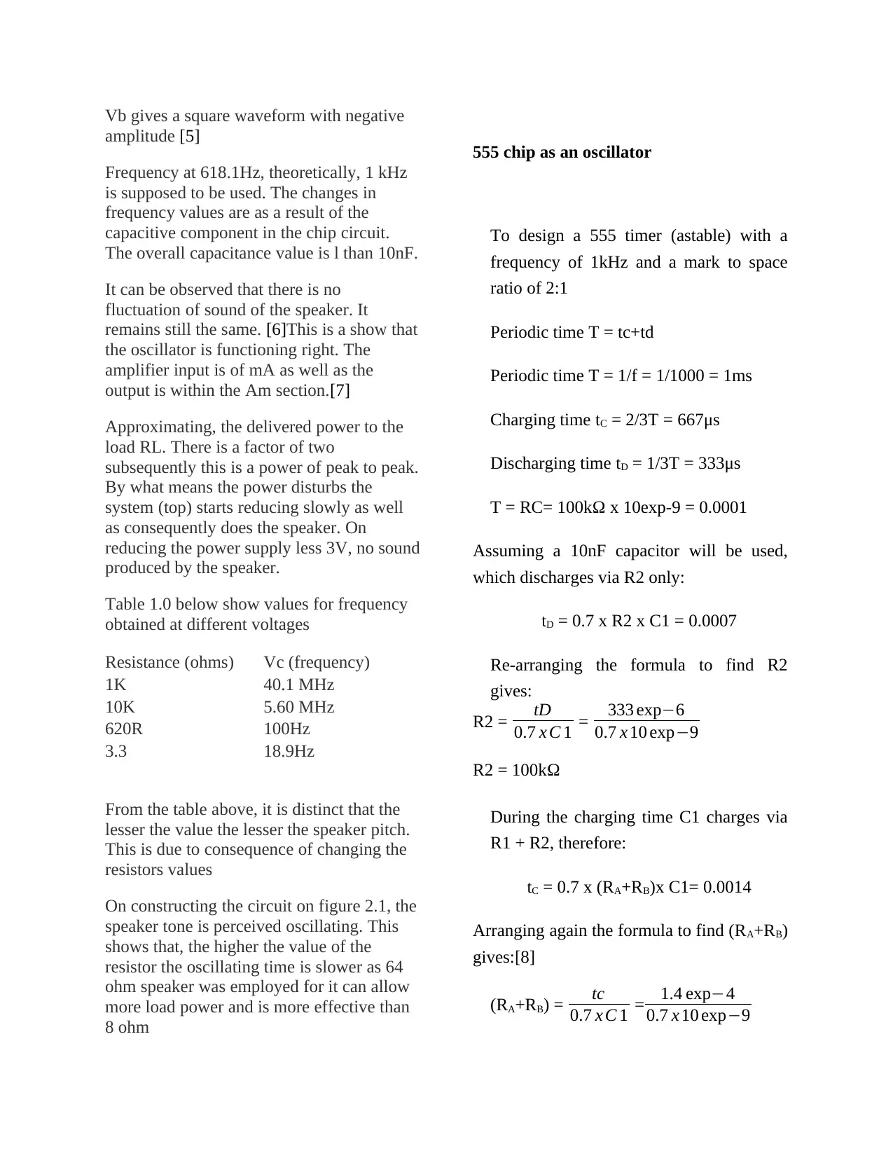
When varying the duty cycle will automatic
change average dc current or dc voltage
output level.
Figure 4a: Duty cycle effects on the DC
level
The Duty Cycle is the mark of the space
ratio of a pulse generator or the square
waves. When varying the duty cycle, it will
automatically change the average dc current
and dc voltage.
At high period of the waveform C1
will charge from high output of RA
till the voltage of pin 6 can reach at
2/3 Vcc which is equal to 6V.
At RB= 330k, the C1 will be
discharged to less than 6 V
depending the timing
It Vcc is reduced to 3V the V out
will be 2volts for C1 will charge at
2/3 of Vcc while the discharge will
be 1V due to RB
Figure 4b: 555 timer oscillator circuit
and waveforms of Vc and Output.
From the experiment the relationship
between Vout = 2/3Vcc.Below are the
waveforms:
RA = (RA+RB) –RB then
RA=200-100= 100kΩ
If the nearest preferred values are chosen for
RA and RB, the values for both resistors
always 100kΩ.In order to check 100kΩ will
provide needed frequency of 1khz; by apply
a frequency formula of 555 astable by using
the values calculated
fosc= 1.4
( R 1+ R 2 ) C 1 = 1.4
200000 x 10 exp−9
=700Hz (while theoretical is 1kHz)[9]
During high charging period the timing, the
capacitor through RA and RB, but is only
RB that can be used when C1 is discharging.
When varying the duty cycle will automatic
change average dc current or dc voltage
output level.
Figure 4a: Duty cycle effects on the DC
level
The Duty Cycle is the mark of the space
ratio of a pulse generator or the square
waves. When varying the duty cycle, it will
automatically change the average dc current
and dc voltage.
At high period of the waveform C1
will charge from high output of RA
till the voltage of pin 6 can reach at
2/3 Vcc which is equal to 6V.
At RB= 330k, the C1 will be
discharged to less than 6 V
depending the timing
It Vcc is reduced to 3V the V out
will be 2volts for C1 will charge at
2/3 of Vcc while the discharge will
be 1V due to RB
Figure 4b: 555 timer oscillator circuit
and waveforms of Vc and Output.
From the experiment the relationship
between Vout = 2/3Vcc.Below are the
waveforms:
⊘ This is a preview!⊘
Do you want full access?
Subscribe today to unlock all pages.
Trusted by 1+ million students worldwide
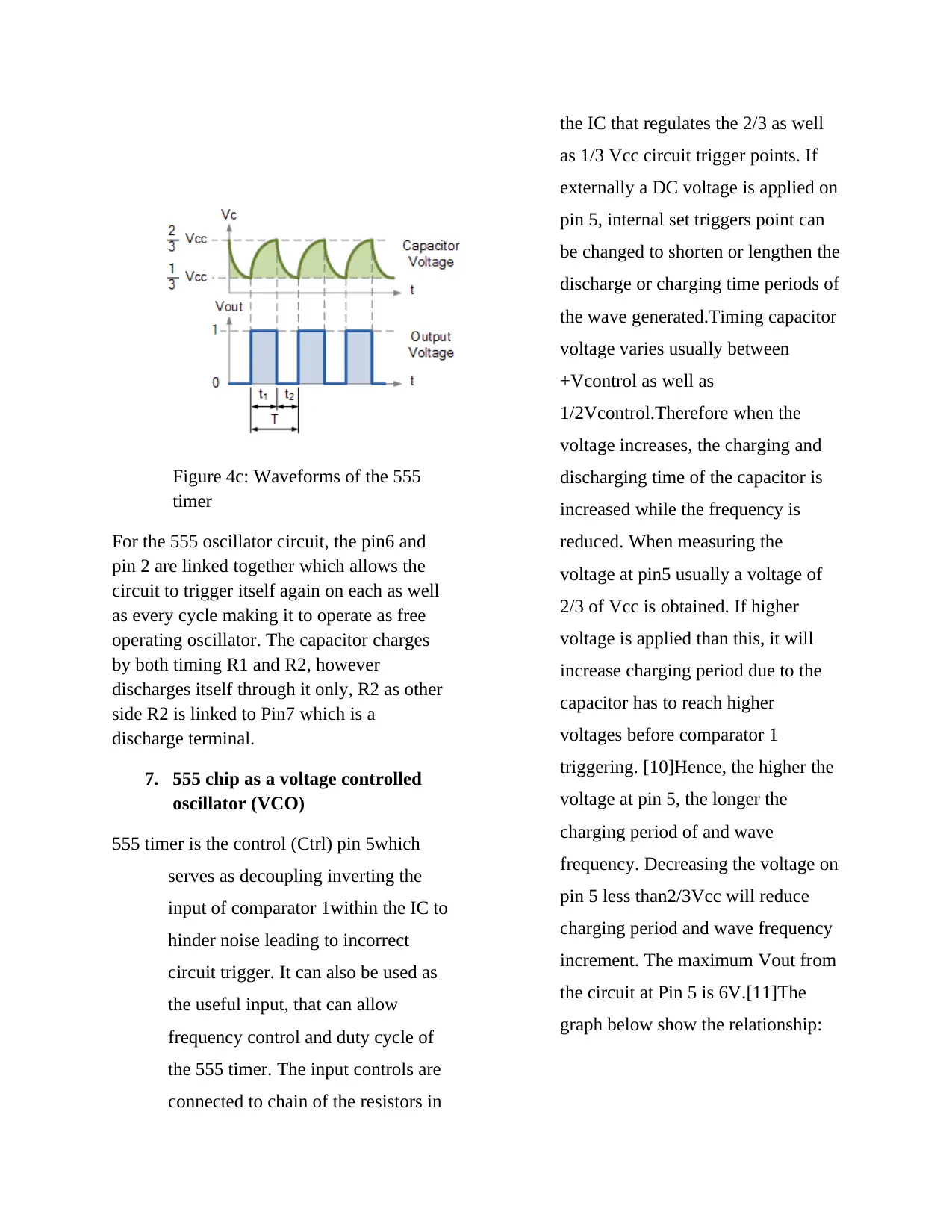
Figure 4c: Waveforms of the 555
timer
For the 555 oscillator circuit, the pin6 and
pin 2 are linked together which allows the
circuit to trigger itself again on each as well
as every cycle making it to operate as free
operating oscillator. The capacitor charges
by both timing R1 and R2, however
discharges itself through it only, R2 as other
side R2 is linked to Pin7 which is a
discharge terminal.
7. 555 chip as a voltage controlled
oscillator (VCO)
555 timer is the control (Ctrl) pin 5which
serves as decoupling inverting the
input of comparator 1within the IC to
hinder noise leading to incorrect
circuit trigger. It can also be used as
the useful input, that can allow
frequency control and duty cycle of
the 555 timer. The input controls are
connected to chain of the resistors in
the IC that regulates the 2/3 as well
as 1/3 Vcc circuit trigger points. If
externally a DC voltage is applied on
pin 5, internal set triggers point can
be changed to shorten or lengthen the
discharge or charging time periods of
the wave generated.Timing capacitor
voltage varies usually between
+Vcontrol as well as
1/2Vcontrol.Therefore when the
voltage increases, the charging and
discharging time of the capacitor is
increased while the frequency is
reduced. When measuring the
voltage at pin5 usually a voltage of
2/3 of Vcc is obtained. If higher
voltage is applied than this, it will
increase charging period due to the
capacitor has to reach higher
voltages before comparator 1
triggering. [10]Hence, the higher the
voltage at pin 5, the longer the
charging period of and wave
frequency. Decreasing the voltage on
pin 5 less than2/3Vcc will reduce
charging period and wave frequency
increment. The maximum Vout from
the circuit at Pin 5 is 6V.[11]The
graph below show the relationship:
Paraphrase This Document
Need a fresh take? Get an instant paraphrase of this document with our AI Paraphraser
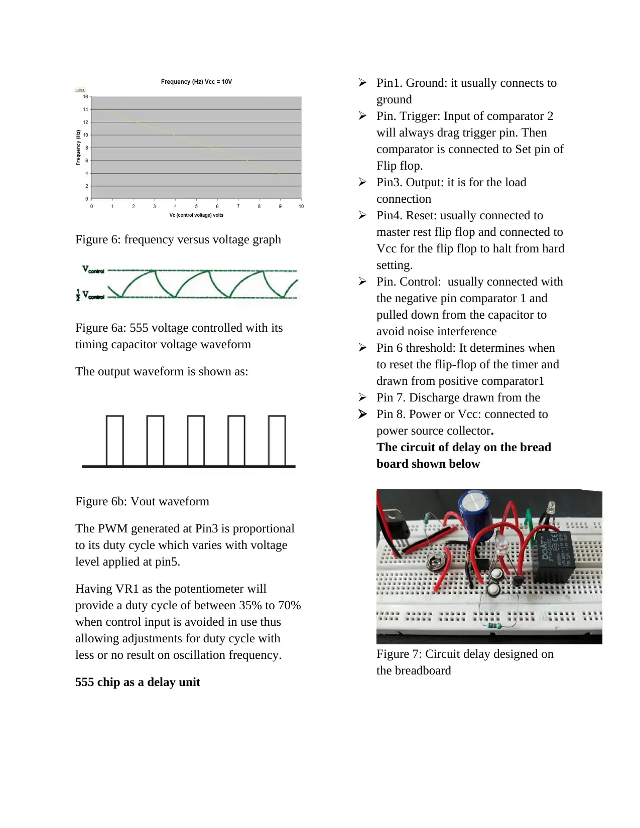
Figure 6: frequency versus voltage graph
Figure 6a: 555 voltage controlled with its
timing capacitor voltage waveform
The output waveform is shown as:
Figure 6b: Vout waveform
The PWM generated at Pin3 is proportional
to its duty cycle which varies with voltage
level applied at pin5.
Having VR1 as the potentiometer will
provide a duty cycle of between 35% to 70%
when control input is avoided in use thus
allowing adjustments for duty cycle with
less or no result on oscillation frequency.
555 chip as a delay unit
Pin1. Ground: it usually connects to
ground
Pin. Trigger: Input of comparator 2
will always drag trigger pin. Then
comparator is connected to Set pin of
Flip flop.
Pin3. Output: it is for the load
connection
Pin4. Reset: usually connected to
master rest flip flop and connected to
Vcc for the flip flop to halt from hard
setting.
Pin. Control: usually connected with
the negative pin comparator 1 and
pulled down from the capacitor to
avoid noise interference
Pin 6 threshold: It determines when
to reset the flip-flop of the timer and
drawn from positive comparator1
Pin 7. Discharge drawn from the
Pin 8. Power or Vcc: connected to
power source collector.
The circuit of delay on the bread
board shown below
Figure 7: Circuit delay designed on
the breadboard
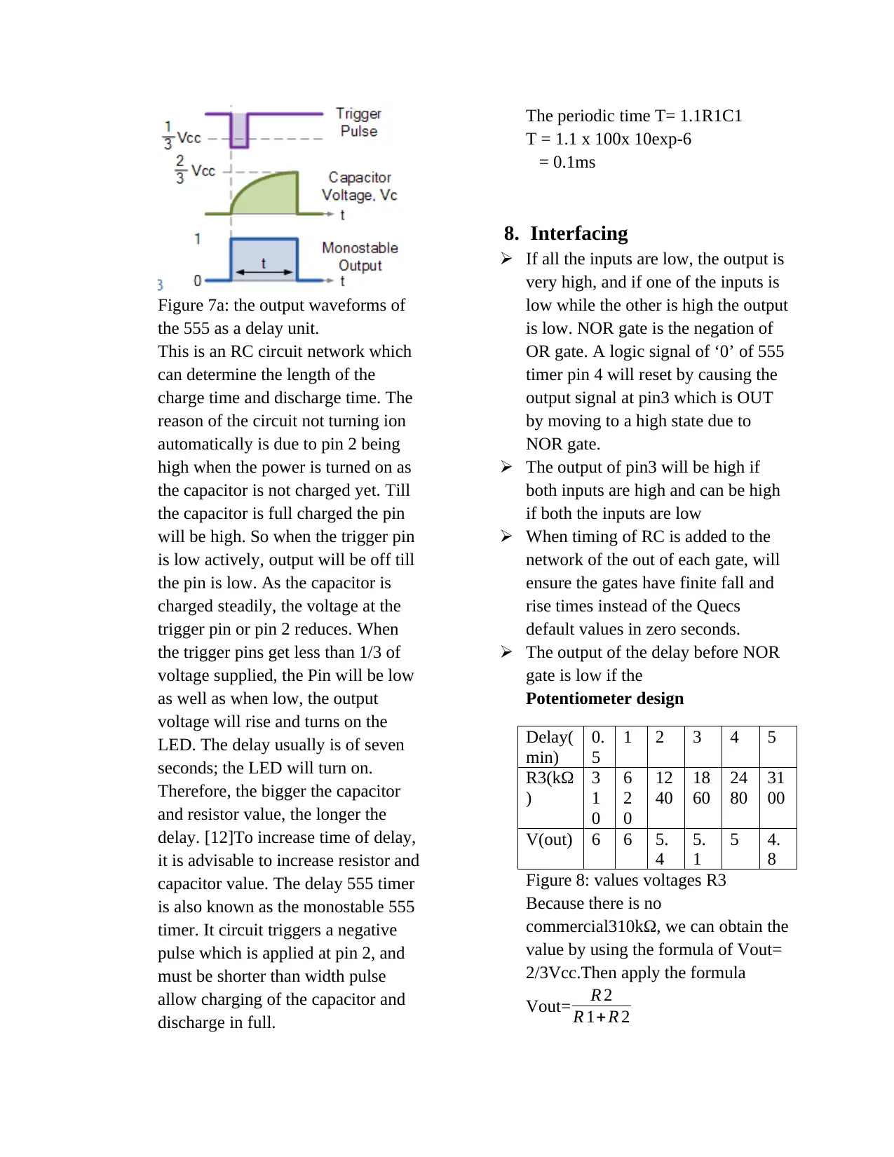
Figure 7a: the output waveforms of
the 555 as a delay unit.
This is an RC circuit network which
can determine the length of the
charge time and discharge time. The
reason of the circuit not turning ion
automatically is due to pin 2 being
high when the power is turned on as
the capacitor is not charged yet. Till
the capacitor is full charged the pin
will be high. So when the trigger pin
is low actively, output will be off till
the pin is low. As the capacitor is
charged steadily, the voltage at the
trigger pin or pin 2 reduces. When
the trigger pins get less than 1/3 of
voltage supplied, the Pin will be low
as well as when low, the output
voltage will rise and turns on the
LED. The delay usually is of seven
seconds; the LED will turn on.
Therefore, the bigger the capacitor
and resistor value, the longer the
delay. [12]To increase time of delay,
it is advisable to increase resistor and
capacitor value. The delay 555 timer
is also known as the monostable 555
timer. It circuit triggers a negative
pulse which is applied at pin 2, and
must be shorter than width pulse
allow charging of the capacitor and
discharge in full.
The periodic time T= 1.1R1C1
T = 1.1 x 100x 10exp-6
= 0.1ms
8. Interfacing
If all the inputs are low, the output is
very high, and if one of the inputs is
low while the other is high the output
is low. NOR gate is the negation of
OR gate. A logic signal of ‘0’ of 555
timer pin 4 will reset by causing the
output signal at pin3 which is OUT
by moving to a high state due to
NOR gate.
The output of pin3 will be high if
both inputs are high and can be high
if both the inputs are low
When timing of RC is added to the
network of the out of each gate, will
ensure the gates have finite fall and
rise times instead of the Quecs
default values in zero seconds.
The output of the delay before NOR
gate is low if the
Potentiometer design
Delay(
min)
0.
5
1 2 3 4 5
R3(kΩ
)
3
1
0
6
2
0
12
40
18
60
24
80
31
00
V(out) 6 6 5.
4
5.
1
5 4.
8
Figure 8: values voltages R3
Because there is no
commercial310kΩ, we can obtain the
value by using the formula of Vout=
2/3Vcc.Then apply the formula
Vout= R 2
R 1+R 2
⊘ This is a preview!⊘
Do you want full access?
Subscribe today to unlock all pages.
Trusted by 1+ million students worldwide
The formula of T = 1.1 R1C1 can be
used to calculate variable resistor
used in design. That is how we can
design the variable resistor by
calculation.
Replace the power supply unit by
a 9V battery
When C5 replaces Vcc will increase
the delay time. In the RC circuits, the
higher the value of the resistor and
capacitor values the longer the delay
time.
When Switch S1 is turned on later
after Switch S2 is turned on first, the
circuit may shot or blow up due to
accumulated charges in the
capacitors. S1 is switched on first,
then S2 is switched on later after
discharge of capacitors.
9. Circuit Design on Veriboard
Schematic Diagram for an electric alarm
Components: 122k potentiometer
(log),11R5 ohm resistor 5% tolerance,110u
25WV electrolytic capacitor2330u,25WV
electrolytic capacitors1100n, ceramic
capacitor 100V,1 LM386 linear integrated
circuit, 1 8 Pin DIL socket.
Circuit diagram below
Figure 9: circuit diagram
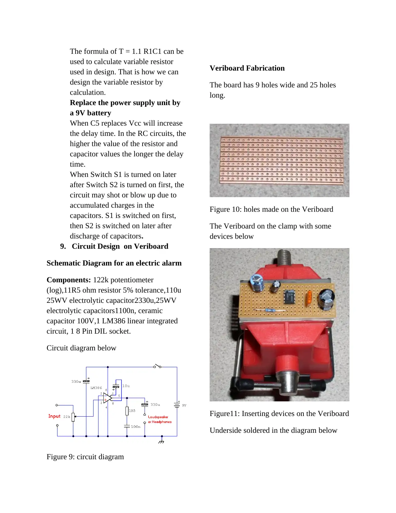
Veriboard Fabrication
The board has 9 holes wide and 25 holes
long.
Figure 10: holes made on the Veriboard
The Veriboard on the clamp with some
devices below
Figure11: Inserting devices on the Veriboard
Underside soldered in the diagram below
used to calculate variable resistor
used in design. That is how we can
design the variable resistor by
calculation.
Replace the power supply unit by
a 9V battery
When C5 replaces Vcc will increase
the delay time. In the RC circuits, the
higher the value of the resistor and
capacitor values the longer the delay
time.
When Switch S1 is turned on later
after Switch S2 is turned on first, the
circuit may shot or blow up due to
accumulated charges in the
capacitors. S1 is switched on first,
then S2 is switched on later after
discharge of capacitors.
9. Circuit Design on Veriboard
Schematic Diagram for an electric alarm
Components: 122k potentiometer
(log),11R5 ohm resistor 5% tolerance,110u
25WV electrolytic capacitor2330u,25WV
electrolytic capacitors1100n, ceramic
capacitor 100V,1 LM386 linear integrated
circuit, 1 8 Pin DIL socket.
Circuit diagram below
Figure 9: circuit diagram
Veriboard Fabrication
The board has 9 holes wide and 25 holes
long.
Figure 10: holes made on the Veriboard
The Veriboard on the clamp with some
devices below
Figure11: Inserting devices on the Veriboard
Underside soldered in the diagram below
Paraphrase This Document
Need a fresh take? Get an instant paraphrase of this document with our AI Paraphraser
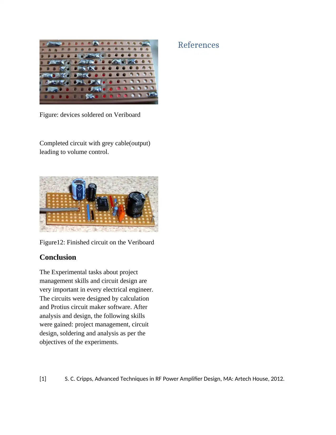
Figure: devices soldered on Veriboard
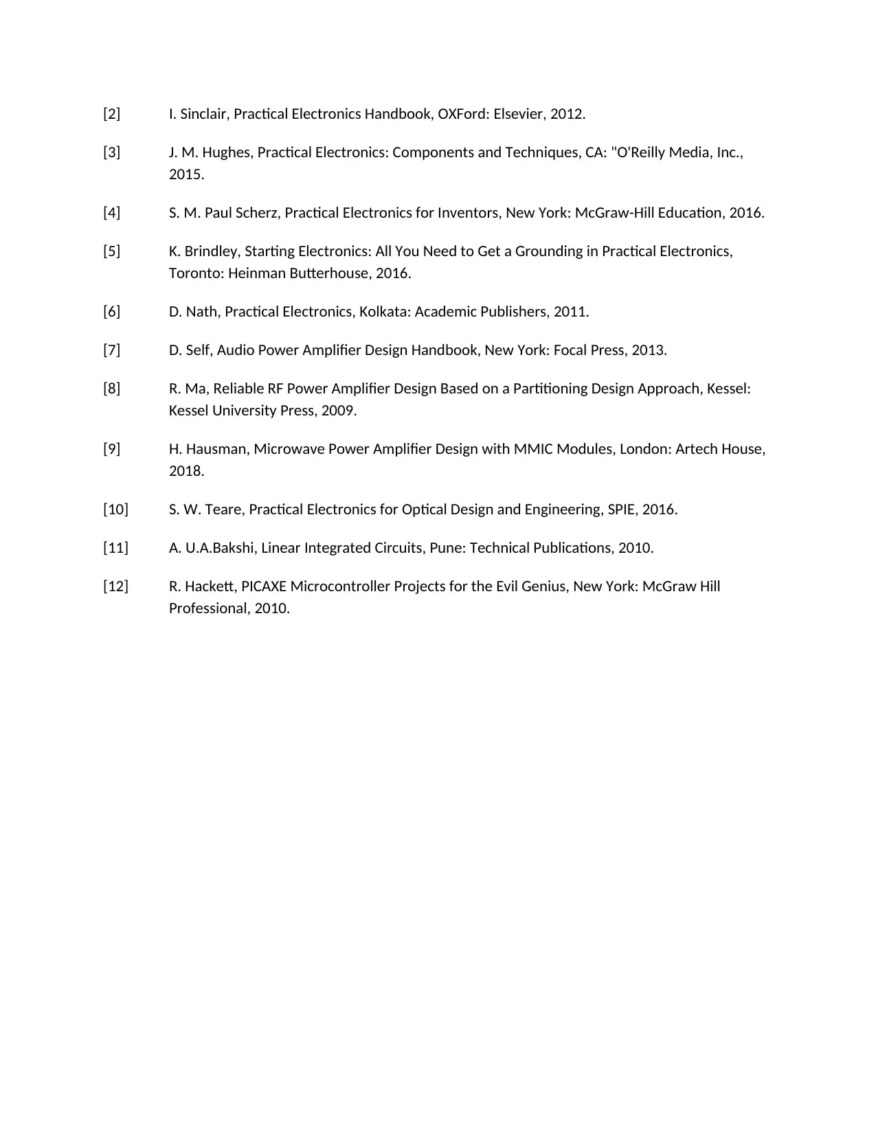
Completed circuit with grey cable(output)
leading to volume control.
Figure12: Finished circuit on the Veriboard
Conclusion
The Experimental tasks about project
management skills and circuit design are
very important in every electrical engineer.
The circuits were designed by calculation
and Protius circuit maker software. After
analysis and design, the following skills
were gained: project management, circuit
design, soldering and analysis as per the
objectives of the experiments.
References
[1] S. C. Cripps, Advanced Techniques in RF Power Amplifier Design, MA: Artech House, 2012.
[2] I. Sinclair, Practical Electronics Handbook, OXFord: Elsevier, 2012.
[3] J. M. Hughes, Practical Electronics: Components and Techniques, CA: "O'Reilly Media, Inc.,
2015.
[4] S. M. Paul Scherz, Practical Electronics for Inventors, New York: McGraw-Hill Education, 2016.
[5] K. Brindley, Starting Electronics: All You Need to Get a Grounding in Practical Electronics,
Toronto: Heinman Butterhouse, 2016.
[6] D. Nath, Practical Electronics, Kolkata: Academic Publishers, 2011.
[7] D. Self, Audio Power Amplifier Design Handbook, New York: Focal Press, 2013.
[8] R. Ma, Reliable RF Power Amplifier Design Based on a Partitioning Design Approach, Kessel:
Kessel University Press, 2009.
[9] H. Hausman, Microwave Power Amplifier Design with MMIC Modules, London: Artech House,
2018.
[10] S. W. Teare, Practical Electronics for Optical Design and Engineering, SPIE, 2016.
[11] A. U.A.Bakshi, Linear Integrated Circuits, Pune: Technical Publications, 2010.
[12] R. Hackett, PICAXE Microcontroller Projects for the Evil Genius, New York: McGraw Hill
Professional, 2010.
⊘ This is a preview!⊘
Do you want full access?
Subscribe today to unlock all pages.
Trusted by 1+ million students worldwide
1 out of 12
Your All-in-One AI-Powered Toolkit for Academic Success.
+13062052269
info@desklib.com
Available 24*7 on WhatsApp / Email
![[object Object]](/_next/static/media/star-bottom.7253800d.svg)
Unlock your academic potential
Copyright © 2020–2026 A2Z Services. All Rights Reserved. Developed and managed by ZUCOL.