EE Project: Design and Simulation of a Flyback Converter
VerifiedAdded on 2022/09/07
|6
|753
|18
Project
AI Summary
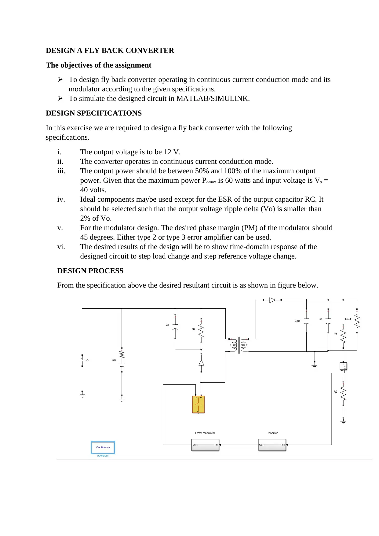
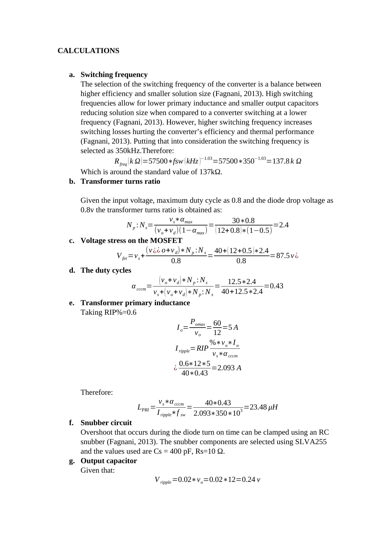
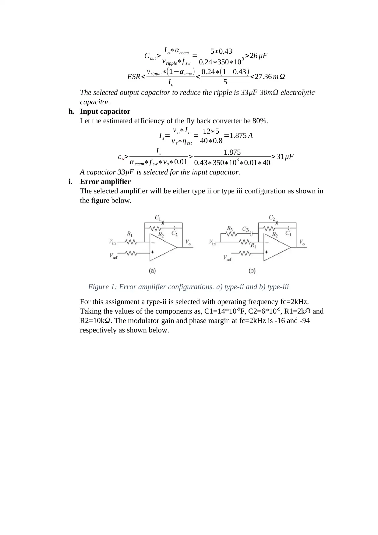
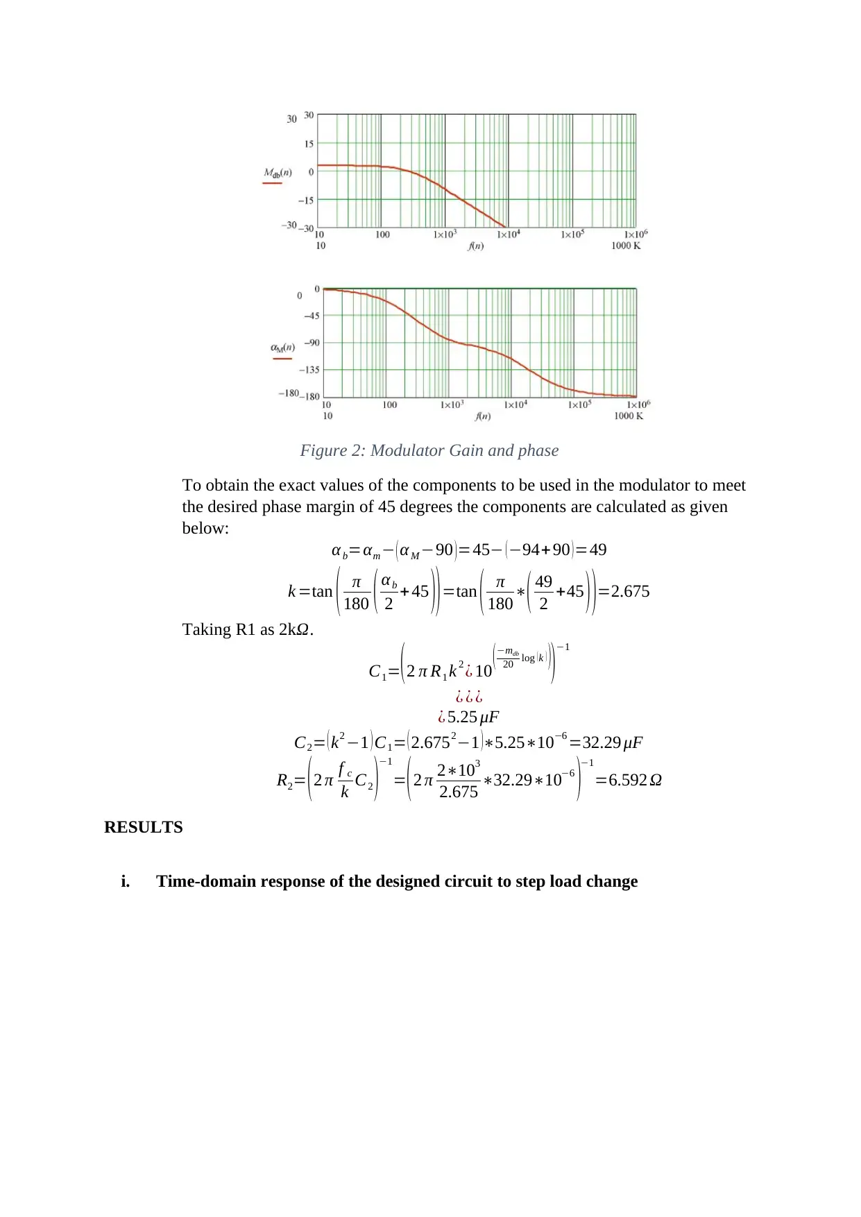
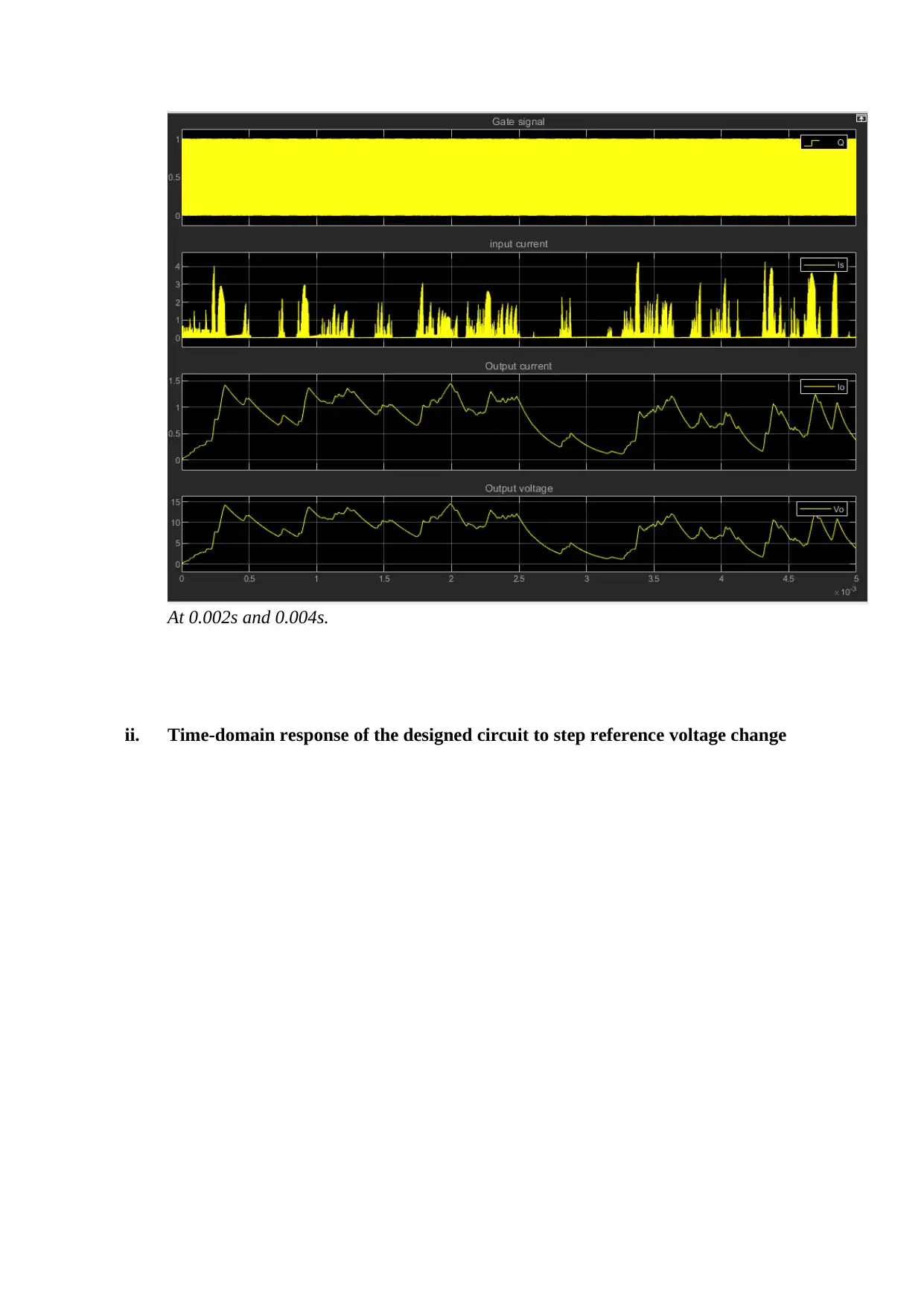
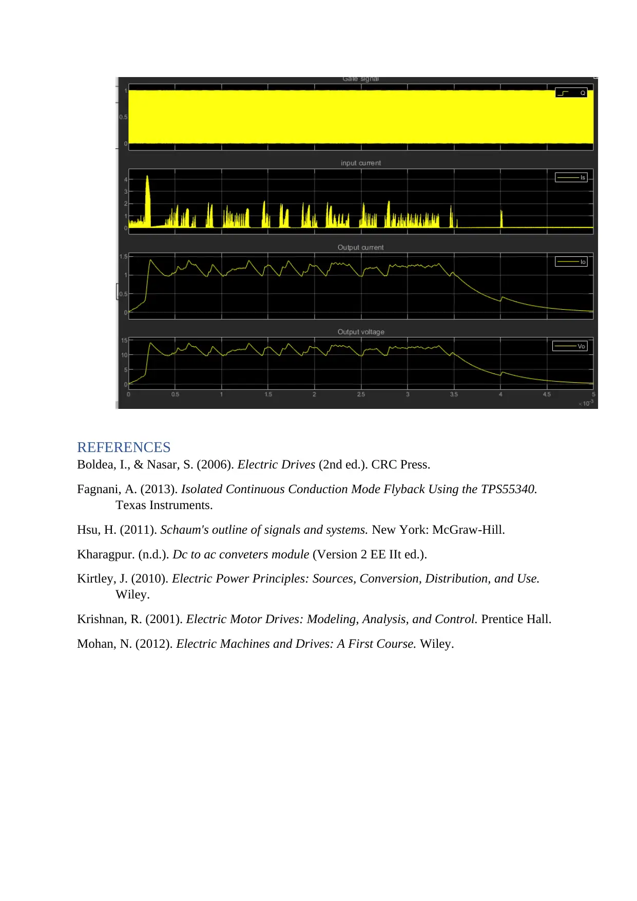
This assignment details the design and simulation of a flyback converter operating in continuous current conduction mode, adhering to specific output voltage, power, and input voltage specifications. The design process involves calculations for switching frequency, transformer turns ratio, MOSFET voltage stress, snubber circuit components, output and input capacitors, and error amplifier configuration. The design utilizes a type-II error amplifier and aims for a 45-degree phase margin. The circuit is simulated in MATLAB/SIMULINK, and the results include time-domain responses to step load changes and step reference voltage changes. References to relevant literature are also provided. This project demonstrates a comprehensive approach to power electronics converter design and simulation, covering key aspects of component selection, circuit analysis, and performance evaluation.

DESIGN A FLY BACK CONVERTER
The objectives of the assignment
To design fly back converter operating in continuous current conduction mode and its
modulator according to the given specifications.
To simulate the designed circuit in MATLAB/SIMULINK.
DESIGN SPECIFICATIONS
In this exercise we are required to design a fly back converter with the following
specifications.
i. The output voltage is to be 12 V.
ii. The converter operates in continuous current conduction mode.
iii. The output power should be between 50% and 100% of the maximum output
power. Given that the maximum power Pomax is 60 watts and input voltage is Vs =
40 volts.
iv. Ideal components maybe used except for the ESR of the output capacitor RC. It
should be selected such that the output voltage ripple delta (Vo) is smaller than
2% of Vo.
v. For the modulator design. The desired phase margin (PM) of the modulator should
45 degrees. Either type 2 or type 3 error amplifier can be used.
vi. The desired results of the design will be to show time-domain response of the
designed circuit to step load change and step reference voltage change.
DESIGN PROCESS
From the specification above the desired resultant circuit is as shown in figure below.
Paraphrase This Document
Need a fresh take? Get an instant paraphrase of this document with our AI Paraphraser

CALCULATIONS
a. Switching frequency
The selection of the switching frequency of the converter is a balance between
higher efficiency and smaller solution size (Fagnani, 2013). High switching
frequencies allow for lower primary inductance and smaller output capacitors
reducing solution size when compared to a converter switching at a lower
frequency (Fagnani, 2013). However, higher switching frequency increases
switching losses hurting the converter’s efficiency and thermal performance
(Fagnani, 2013). Putting that into consideration the switching frequency is
selected as 350kHz.Therefore:
Rfreq ( k Ω )=57500∗fsw ( kHz )−1.03=57500∗350−1.03=137.8 k Ω
Which is around the standard value of 137kΩ.
b. Transformer turns ratio
Given the input voltage, maximum duty cycle as 0.8 and the diode drop voltage as
0.8v the transformer turns ratio is obtained as:
N p : Ns= vs∗αmax
(vo + vd )(1−αmax )= 30∗0.8
( 12+0.8 )∗(1−0.5) =2.4
c. Voltage stress on the MOSFET
V fet =vs +(v ¿¿ o+v d)∗N p :N s
0.8 = 40+ ( 12+0.5 )∗2.4
0.8 =87.5 v ¿
d. The duty cycles
α cccm= ( vo + vd ) ∗N p : Ns
vs + ( vo +vd ) ∗N p : N s
= 12.5∗2.4
40+12.5∗2.4 =0.43
e. Transformer primary inductance
Taking RIP%=0.6
I o= Pomax
vo
= 60
12 =5 A
I ripple=RIP %∗vo∗I o
vs∗α cccm
¿ 0.6∗12∗5
40∗0.43 =2.093 A
Therefore:
LPRI = vs∗αcccm
I ripple∗f sw
= 40∗0.43
2.093∗350∗103 =23.48 μH
f. Snubber circuit
Overshoot that occurs during the diode turn on time can be clamped using an RC
snubber (Fagnani, 2013). The snubber components are selected using SLVA255
and the values used are Cs = 400 pF, Rs=10 Ω.
g. Output capacitor
Given that:
V ripple =0.02∗vo=0.02∗12=0.24 v

Cout > Io∗αcccm
vripple∗f sw
= 5∗0.43
0.24∗350∗103 >26 μF
ESR < vripple∗(1−αmax )
Io
< 0.24∗(1−0.43)
5 <27.36 m Ω
The selected output capacitor to reduce the ripple is 33μF 30mΩ electrolytic
capacitor.
h. Input capacitor
Let the estimated efficiency of the fly back converter be 80%.
I s= v o∗Io
v s∗ηest
= 12∗5
40∗0.8 =1.875 A
c¿> Is
α cccm∗f sw∗vs∗0.01 > 1.875
0.43∗350∗103∗0.01∗40 > 31 μF
A capacitor 33μF is selected for the input capacitor.
i. Error amplifier
The selected amplifier will be either type ii or type iii configuration as shown in
the figure below.
Figure 1: Error amplifier configurations. a) type-ii and b) type-iii
For this assignment a type-ii is selected with operating frequency fc=2kHz.
Taking the values of the components as, C1=14*10-9F, C2=6*10-9, R1=2kΩ and
R2=10k Ω. The modulator gain and phase margin at fc=2kHz is -16 and -94
respectively as shown below.
⊘ This is a preview!⊘
Do you want full access?
Subscribe today to unlock all pages.

Trusted by 1+ million students worldwide

Figure 2: Modulator Gain and phase
To obtain the exact values of the components to be used in the modulator to meet
the desired phase margin of 45 degrees the components are calculated as given
below:
α b=αm − ( α M −90 )=45− (−94+ 90 )=49
k =tan ( π
180 ( α b
2 + 45 ))=tan ( π
180∗( 49
2 +45 ) )=2.675
Taking R1 as 2kΩ.
C1=(2 π R1 k 2 ¿ 10 (−mdb
20 log (k ) ))−1
¿ ¿ ¿
¿ 5.25 μF
C2= ( k2 −1 ) C1= ( 2.6752−1 )∗5.25∗10−6 =32.29 μF
R2= (2 π f c
k C2 )−1
=(2 π 2∗103
2.675 ∗32.29∗10−6
)−1
=6.592 Ω
RESULTS
i. Time-domain response of the designed circuit to step load change
Paraphrase This Document
Need a fresh take? Get an instant paraphrase of this document with our AI Paraphraser

At 0.002s and 0.004s.
ii. Time-domain response of the designed circuit to step reference voltage change

REFERENCES
Boldea, I., & Nasar, S. (2006). Electric Drives (2nd ed.). CRC Press.
Fagnani, A. (2013). Isolated Continuous Conduction Mode Flyback Using the TPS55340.
Texas Instruments.
Hsu, H. (2011). Schaum's outline of signals and systems. New York: McGraw-Hill.
Kharagpur. (n.d.). Dc to ac conveters module (Version 2 EE IIt ed.).
Kirtley, J. (2010). Electric Power Principles: Sources, Conversion, Distribution, and Use.
Wiley.
Krishnan, R. (2001). Electric Motor Drives: Modeling, Analysis, and Control. Prentice Hall.
Mohan, N. (2012). Electric Machines and Drives: A First Course. Wiley.
⊘ This is a preview!⊘
Do you want full access?
Subscribe today to unlock all pages.

Trusted by 1+ million students worldwide
1 out of 6
Related Documents

Your All-in-One AI-Powered Toolkit for Academic Success.
+13062052269
info@desklib.com
Available 24*7 on WhatsApp / Email
Unlock your academic potential
Copyright © 2020–2025 A2Z Services. All Rights Reserved. Developed and managed by ZUCOL.