Comprehensive Report on Laser Diodes: Working, Application

Verified

Added on  2023/06/14

|7
|1025
|264
Report
AI Summary
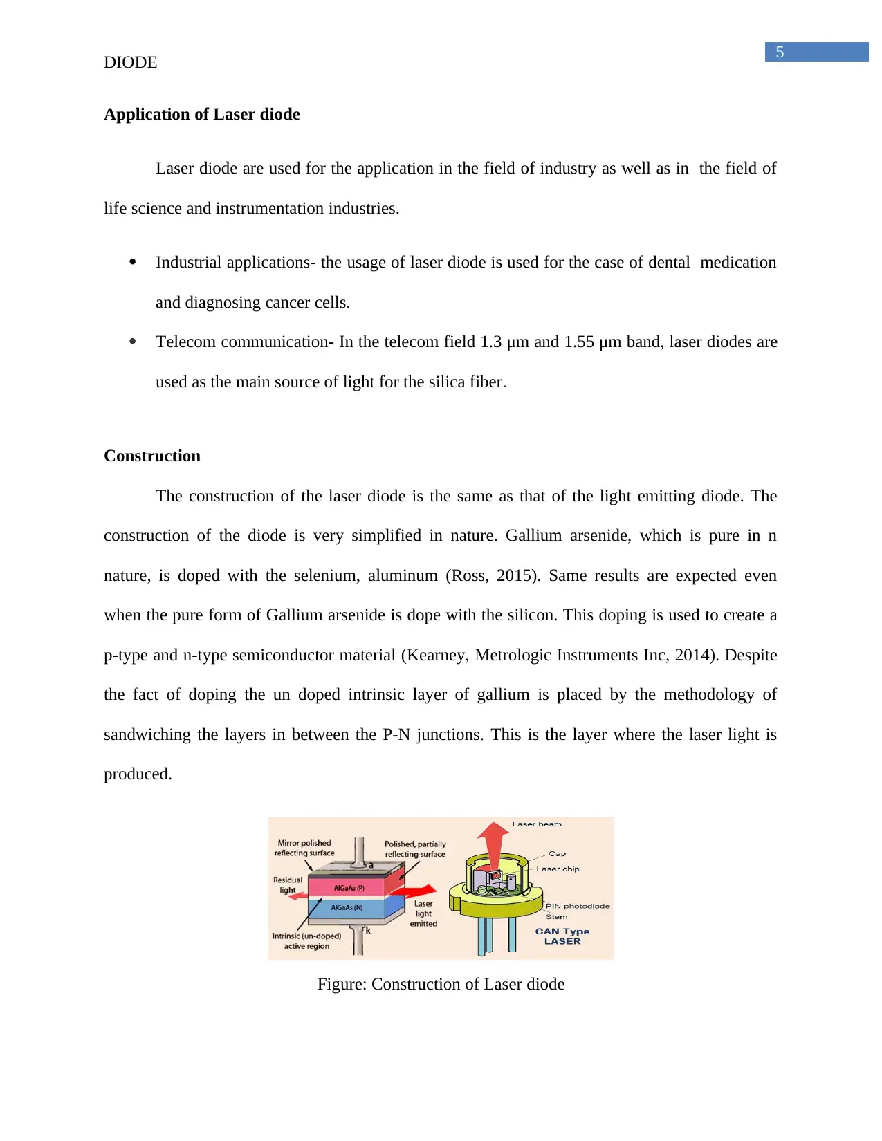
This report provides an overview of laser diodes, starting with the basic definition and unidirectional properties of diodes. It delves into the specifics of laser diodes, including their invention, working principles involving photon oscillation between p-type and n-type semiconductors, and the three key steps: energy absorption, spontaneous emission, and stimulated emission. The report highlights applications in industries such as dental medication, cancer diagnosis, and telecommunications, where they serve as light sources for silica fiber. The construction of laser diodes is also discussed, detailing the doping process of Gallium arsenide with selenium or aluminum to create p-type and n-type semiconductor materials and the placement of an intrinsic layer between the P-N junctions where laser light is produced.
Document Page
Running Head: DIODE
Diode
Name of the Student
Name of the University
Authors Note
tabler-icon-diamond-filled.svg

Paraphrase This Document

Need a fresh take? Get an instant paraphrase of this document with our AI Paraphraser
Document Page
2
DIODE
Table of Contents
Diode................................................................................................................................................3
Laser diode...................................................................................................................................3
Working...................................................................................................................................3
Application of Laser diode..........................................................................................................5
Construction.....................................................................................................................................5
Reference.........................................................................................................................................6
Document Page
3
DIODE
Diode
Diode is an electronic device that is supposedly two dimensional in nature. This property
of diode ensured that there is flow of current in one direction only. This property of diode makes
them unidirectional in nature (Grundmann, 2015). The basic purpose of the diodes is to rectify
the waveforms that are in the present in the radio detectors or are present in the power supplies.
Diodes finds there importance in the circuits where the requirements of the circuits are to flow
the current only in one direction.
Laser diodes has been one of the most important diode is used in the market due t its application.
Laser diode
Laser diode is the semiconductor laser that highly resembles with the light emitting
diode. Dr. Robert Hall invented the ladser diode in the year 1962. The diode’s main function is to
emit laser beam form by bouncing the photons and putting it in the oscillatory motion (Chichibu
and Nakamura, 2014). The bounce of the photon is made in between the positive and the
negative type semiconductor that is kept at a distance of one micrometer. This technology uses
process same as the conventional lasers. This used to pump the photons repetitively in between
two mirror slices, which emitted laser beam of light. Laser diode is a forward biased diode,
which has two carriers namely the holes and the electrons. The forward biasing done in the
diodes enables the electron and the hole are pumped on to the opposite side of the p-n junction
into the depleted side of the diode that has charge carriers present. Due to the fact of injecting the
charged particles for the flow of charge it is known as the injection laser diodes.
Working
The working of the laser diode requires three main steps, they are namely: -
Document Page
4
DIODE
Energy absorption
The laser diode basically has a p-n junction in which the holes of the diode and the electrons
of the diode dwells. Holes is nothing but the absence of the electron in the diode is termed as the
holes. When a particular voltage is applied to the p-n junction, the injected en energy is absorbed
by the negatively charged electron which gets charged up and the transition process begins. This
transition takes the electron to the higher level. The electron that move to the higher level stay
their without combining with the holes for few nano seconds.
Spontaneous emission
After the electrons complete the lifeline of staying in the upper level without combining with
the holes the electrons fall apart t the lower energy level the energy that is released during the
electron the fell from the higher energy level produces the charge of the photon (Petermann,
2018). This process of producing the electron radiation is also used for the production of light in
light emission diodes. The energy that is transferred to the photon is due to the energy level
differences.
Stimulated emission
Coherent photons more than one are needed from the laser diode for this process than that of
the spontaneous emission process. Two mirror are placed in the either sides of the p-n junction
this ensured that the charge gets strides in the process (Ghafouri-Shiraz, 2016). This causes the
fact of combination of the electron with the holes due to the charge that has been produced by the
photon. When the concentration level reaches the threshold level the bright monochromatic light
is produced.
tabler-icon-diamond-filled.svg

Paraphrase This Document

Need a fresh take? Get an instant paraphrase of this document with our AI Paraphraser
Document Page
5
DIODE
Application of Laser diode
Laser diode are used for the application in the field of industry as well as in the field of
life science and instrumentation industries.
Industrial applications- the usage of laser diode is used for the case of dental medication
and diagnosing cancer cells.
Telecom communication- In the telecom field 1.3 μm and 1.55 μm band, laser diodes are
used as the main source of light for the silica fiber.
Construction
The construction of the laser diode is the same as that of the light emitting diode. The
construction of the diode is very simplified in nature. Gallium arsenide, which is pure in n
nature, is doped with the selenium, aluminum (Ross, 2015). Same results are expected even
when the pure form of Gallium arsenide is dope with the silicon. This doping is used to create a
p-type and n-type semiconductor material (Kearney, Metrologic Instruments Inc, 2014). Despite
the fact of doping the un doped intrinsic layer of gallium is placed by the methodology of
sandwiching the layers in between the P-N junctions. This is the layer where the laser light is
produced.
Figure: Construction of Laser diode
Document Page
6
DIODE
Reference
Chichibu, S.F. and Nakamura, S., 2014. Introduction to nitride semiconductor blue lasers and
light emitting diodes. CRC Press.
Ghafouri-Shiraz, H., 2016. Fundamentals of laser diode amplifiers. J. Wiley,
Grundmann, M., 2015. The Physics of Semiconductors: An Introduction Including Nanophysics
and Applications. Springer.
Kearney, S.P., Metrologic Instruments Inc, 2014. Method of and apparatus for multiplying raster
scanning lines by modulating a multi-cavity laser diode. U.S. Patent 8,678,285.
Petermann, K., 2018. Laser diode modulation and noise (Vol. 3). Springer Science & Business
Media.
Ross, M., 2015. YAG laser operation by semiconductor laser pumping. Proceedings of the
IEEE, 56(2), pp.196-197.
Document Page
7
DIODE
chevron_up_icon
1 out of 7
circle_padding
hide_on_mobile
zoom_out_icon
[object Object]