Design and Implementation of a Low Noise RF Amplifier Project (ECE307)
VerifiedAdded on 2022/08/20
|18
|4156
|12
Project
AI Summary
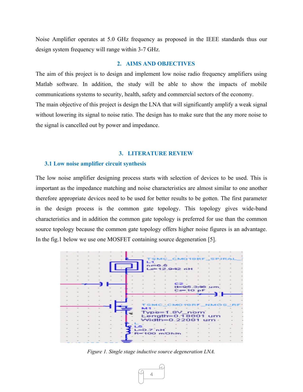
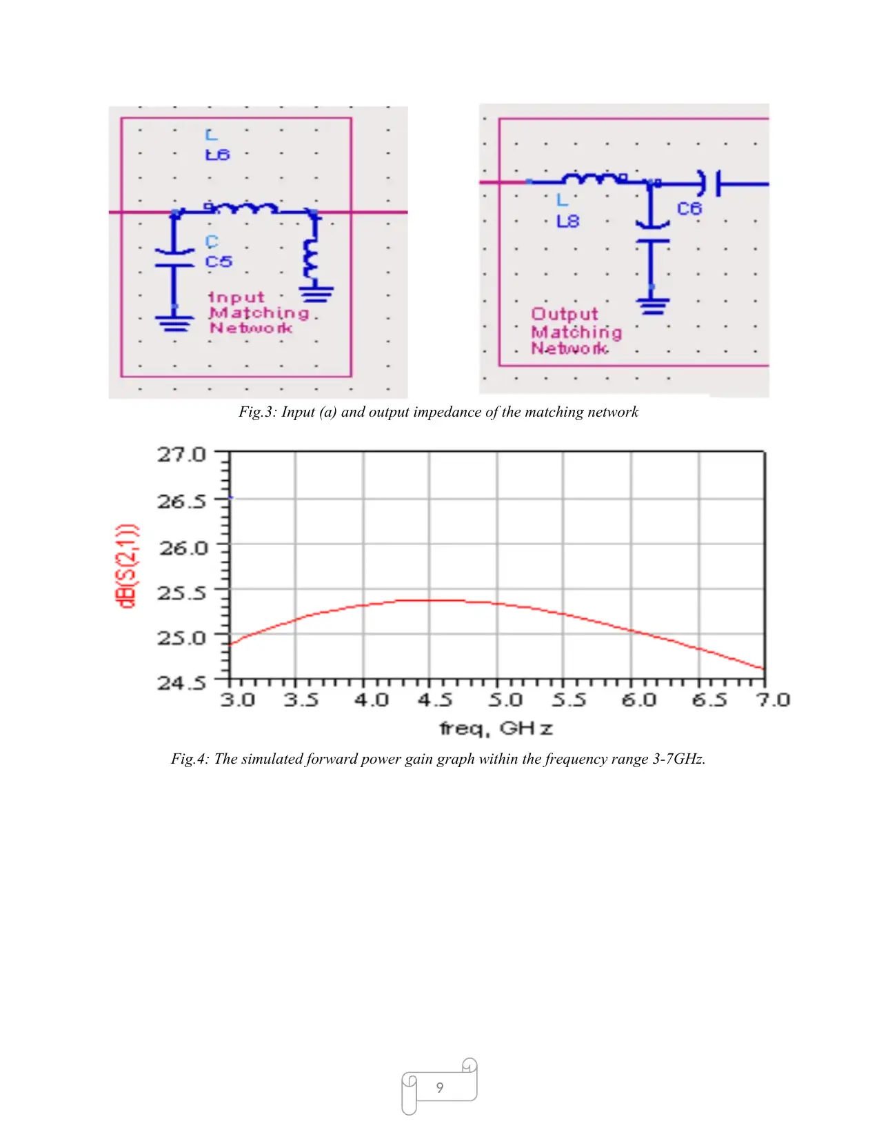
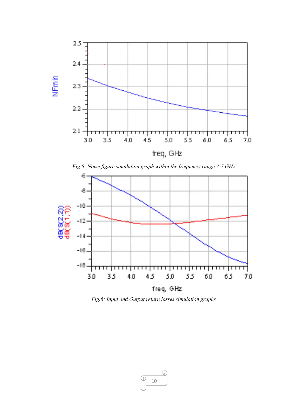
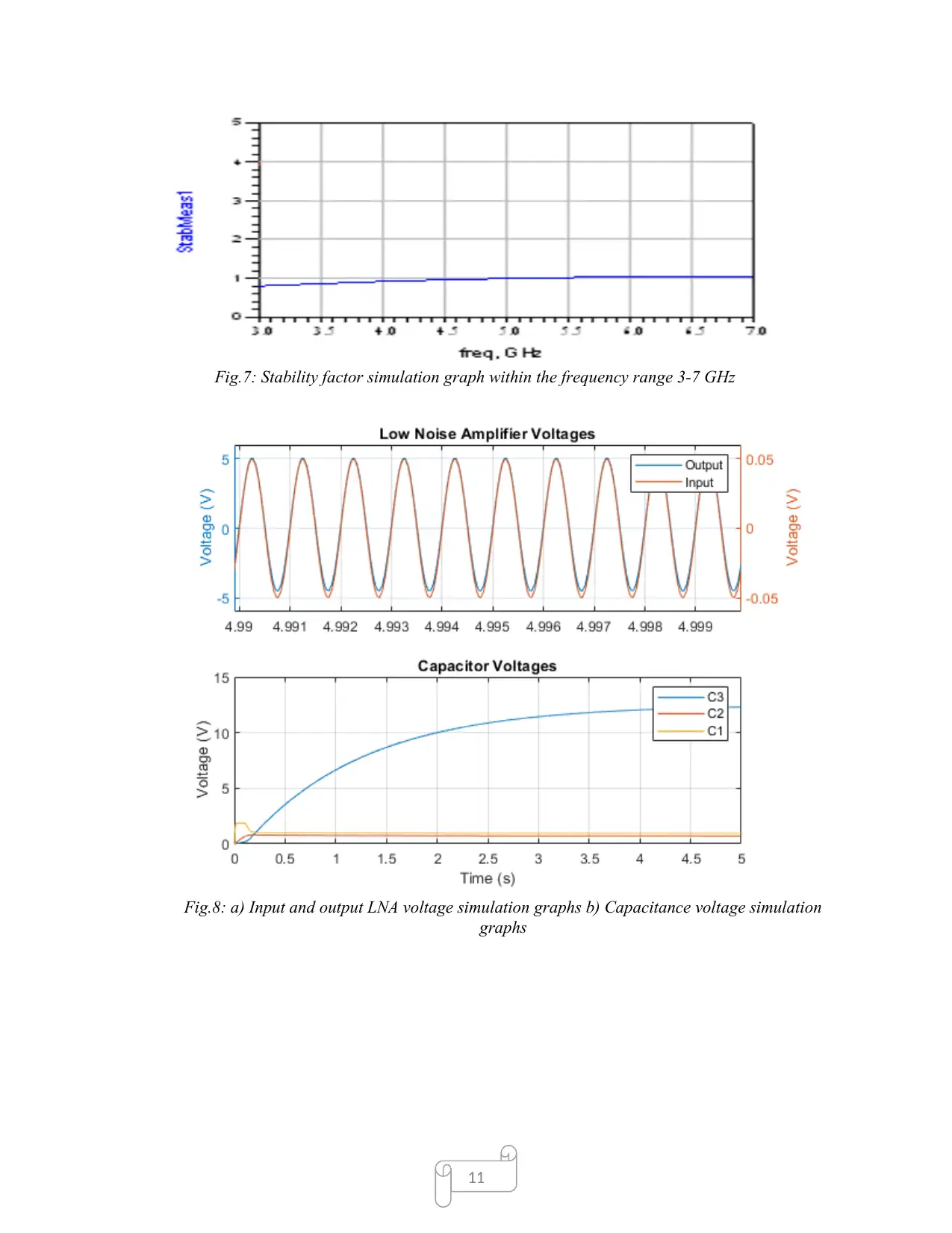
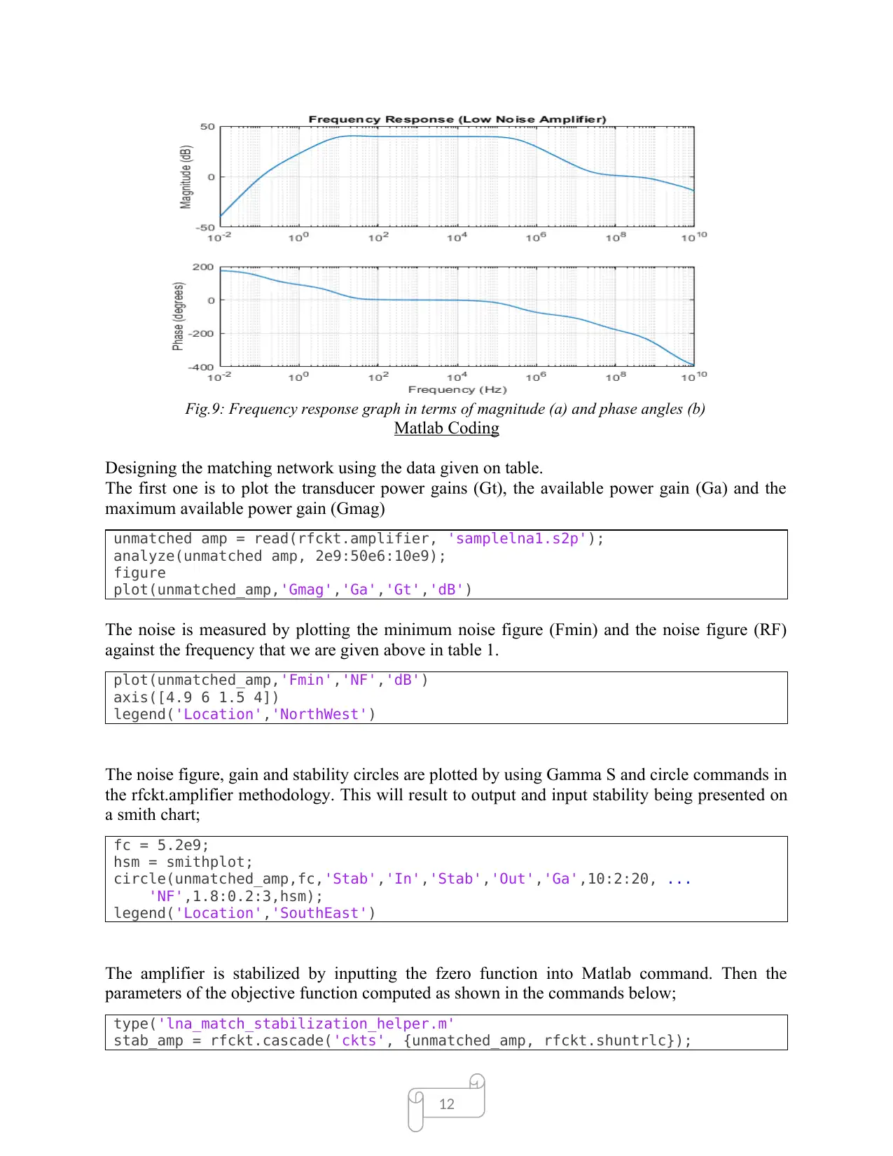
This project details the design and implementation of a low noise RF amplifier (LNA) for use in radio frequency receiver systems. The project focuses on designing an LNA with high power gain and low noise within the 3-7 GHz frequency range, utilizing inductive source degeneration and cascode topology with MOSFETs. The design incorporates components like inductors and capacitors to achieve a 50 Ω input impedance. The project includes detailed calculations for parameters like noise figure, stability, and matching networks. The design is simulated using Matlab, with results presented through graphs illustrating forward power gain, noise figure, input/output return losses, and stability factors. The report also provides an overview of the design process, including literature review, aims, objectives, and a discussion of key concepts like DC biasing and single-stage amplifier design. The project emphasizes the importance of LNA in communication systems, especially for amplifying weak signals while minimizing noise, and also touches upon the impact of mobile communication systems on various sectors. Matlab coding for the design of matching networks and the analysis of amplifier performance is also provided.

1
DESIGN AND IMPLEMENTATION OF LOW NOISE RF
AMPLIFIERS
Abstract: Low noise RF amplifiers (LNA) are found in all radio frequency receiver in mobile
communication systems. They are defined as the front end block in the RF receiver system which
powers or amplifies the weak signal that is received by antenna and increases the signal to noise
ration to over the normal noise floor. The design of the low noise amplifier involves
determination of various parameters required which include power gain, noise figure, insertion
losses and power consumption of the communication receiver system. This project will try to
design the low noise amplifier which meets the criteria that has been specified. The design
proposal will be of a single low noise RF amplifier that is having high power gain and low noise.
It will use the inductive source reduction mechanism within the frequency ranges of 3GHz and
7GHz. In addition there are various devices that will be used in the system design which include
inductors and capacitors. They will be used in achieving 50 Ω input impedance which will have
low noise factor. This design will be simulated and run using Matlab software.
Keywords: Advanced design system. Low noise amplifier. Radio-frequency. Noise figure.
Wireless network.
Paraphrase This Document
Need a fresh take? Get an instant paraphrase of this document with our AI Paraphraser

2
Table of Contents
Introduction 2
Aims and Objectives 3
Literature Review 3
Low noise amplifier circuit synthesis 4
DC Biasing 5
Single stage amplifier 6
Noise figure 7
Stability 8
Design simulations and Results 9
Matching networks 10
Risk factors of Mobile communications 14
Conclusion 15
References 16
Appendix 18
Table of Figures
Figure No. Description Page No.
1 Showing inductive source with single stage amplifier 8
2 The DC biasing network using an active device 12
3 Input (a) and output impedance of the matching network 13
4 The simulated forward power gain graph within the frequency
range 3-7GHz
13
5 Noise figure simulation graph within the frequency range 3-7
GHz
14
6 Input and Output return losses simulation graphs 14
7 Stability factor simulation graph within the frequency range 3-7
GHz
16
8 a) Input and output LNA voltage simulation graphs
b) Capacitance voltage simulation graphs
16
9 Frequency response graph in terms of magnitude (a) and phase
angles (b)
16

3
1. INTRODUCTION
Communication systems have been made efficient due to invention of use of the low noise
amplifiers (LNA). The LNA have become an important component of the communication system
especially the receiving end of it where the LNA acts as the front end block in the receiving
system of communication [1]. Measuring of the low noise amplifier is done in terms of the
following parameters; dynamic range, return loss, stability circles and many more. In mobile
communication systems the transmitted signal is received by the antenna at the receiving end.
This is rendered weak or low power due to losses incurred within the communication system and
the space which includes system loss, atmospheric attenuation, depointing losses and many other
factors. Thus the weak signal need to be boosted to regain the power and reduce noise. In this
design, two MOSFETs are employed in designing the cascode topology [2].
The design implemented using cascode topology with MOSFETs is more efficient as there is
high impedance both input and output. Due to this the device design parameters the mentioned
two MOSFETs in cascode topology can therefore be implemented separately with little trade-off.
Cascode topology is a situation in circuits where the amplifier loads are connected in a vertical
configuration. The disadvantage of this type of topology is that larger area is needed and is more
complex than the cascade topology. In this topology though, the parameters can be set to provide
with high input signal powers of up to 15 dBm without getting the system linearity degraded or
destroyed and in addition this topology does not add more noise to the system [3]. Therefore in
this topology, the wireless communication receiver is able to work even in very hostile
environments.
In this design, the low noise RF amplifier design, the discussed parameters which impact mobile
communication are forward, stability circle, low noise and matching networks. Our project
encompasses designing a CMOS low noise amplifier by the use of single stage inductive source
degenerative topology in relation to the optimization of noise and matching of impedances. We
employ cascode topology amplifier design system in designing our low noise amplifier. The
design process involves employing the inductive degeneration common source topology together
with active device biasing. Incorporating active devices into our design system will lead to
increasing temperature sensitivity of the amplifier which is beneficial [4]. The proposed Low
⊘ This is a preview!⊘
Do you want full access?
Subscribe today to unlock all pages.

Trusted by 1+ million students worldwide

4
Noise Amplifier operates at 5.0 GHz frequency as proposed in the IEEE standards thus our
design system frequency will range within 3-7 GHz.
2. AIMS AND OBJECTIVES
The aim of this project is to design and implement low noise radio frequency amplifiers using
Matlab software. In addition, the study will be able to show the impacts of mobile
communications systems to security, health, safety and commercial sectors of the economy.
The main objective of this project is design the LNA that will significantly amplify a weak signal
without lowering its signal to noise ratio. The design has to make sure that the any more noise to
the signal is cancelled out by power and impedance.
3. LITERATURE REVIEW
3.1 Low noise amplifier circuit synthesis
The low noise amplifier designing process starts with selection of devices to be used. This is
important as the impedance matching and noise characteristics are almost similar to one another
therefore appropriate devices need to be used for better results to be gotten. The first parameter
in the design process is the common gate topology. This topology gives wide-band
characteristics and in addition the common gate topology is preferred for use than the common
source topology because the common gate topology offers higher noise figures is an advantage.
In the fig.1 below we use one MOSFET containing source degeneration [5].
Figure 1. Single stage inductive source degeneration LNA.
Paraphrase This Document
Need a fresh take? Get an instant paraphrase of this document with our AI Paraphraser

5
The minimum noise factor, NF can be set to not depend on the width of the transistors by using
the source degeneration reactance instead [6]. Thus the input impedance can be calculated as
follows;
Z¿= V ¿
I ¿
=S ( LG +LS ) + 1
s Cgs
+ gm Ls
Cgs
The reactance Ls can be calculated using the following formula, when using the impedance as 50
ohms;
Ls =Cgs
gm
Zo
The low noise amplifier design calculations and formula are in reference to the IEEE standards
set. This amplifier is designed by involving the devices’ noise characteristics and parameters as
shown in the design. In our case, we realign the input of the transistor to match with input
impedance so than the noise figure, NF is optimized and the output of the transistor is also
matched with the system impedance which is 50 ohms so than the gain is maximized [7].
Therefore, the noise figure, NF, of a two port network is calculated using the formula shown
below;
NO =FGKTB
For instance, if the minimum input signal given is X dB above the noise floor, then power gain is
given as;
P¿
Min=N o−G+ X
POut
Min=N o + X
3.2 DC Biasing
In the design process the design system temperature can maintained by proper biasing whereby
the current is kept constant despite parameter variations in the design system. In the design the
preferred device parameter used for biasing is I dss which is the saturated current at zero gate [8].

6
Transconductance is defined as the change of ID in relation to V G voltage, and is given by the
formula;
In normal amplifier system design, either active or passive biasing can be used but in our design
we introduced also the active component for the biasing process at the voltage of 2.14 V. the DC
biasing system is as shown below in fig.2;
Figure 2. Active device DC biasing network.
3.3 Single Stage Amplifier
A sing stage amplifier is composed of a transistor, a circuit that is used for matching the source
termination, and another transistor that is employed to match the load termination and the initial
transistor. In our design of the low noise amplifier we set the source and the load terminations at
50 ohms. In the design also, we use the transducer power to take care of the mismatching likely
to arise at both source and load [9]. The system transistor of our design is set to work properly
when both load and source conditions are appropriate for the design by matching the two circuits
as shown in in fig.1 above. Matching occurs when Z ( jωo ) =Rs and it is given by;
(L¿¿ G+ LS )W O= 1
W O Cgs
¿
Rs= gm Ls
Cgs
⊘ This is a preview!⊘
Do you want full access?
Subscribe today to unlock all pages.

Trusted by 1+ million students worldwide

7
Where RS is the resistor put at the source of input voltage.
3.4 Noise figure
In design calculations the total noise power refers to the powered input noise that is coming into
the amplifier and the noise generated at the amplifier itself. Therefore the total noise bandwidth
(NBW) is calculated using the formula shown below; in design calculations the total noise power
refers to the powered input noise that is coming into the amplifier and the noise generated at the
amplifier itself [10]. Therefore the total noise bandwidth (NBW) is calculated using the formula
shown below;
The noise bandwidth range is limited in the amplifier system by other available components.
Therefore the noise figure, NF, is given by [22];
In our design system, the total equivalent input current refers to all noise caused by reflected
drain and the current noise caused at the induced gate in the design system. The other
characteristics of noise can be calculated using the formula;
In addition, we can calculate the minimum noise figure using the formula [23];
3.5 Stability
The stability of the circuit of our system design is represented by determining the stern stability
factor (K) [11]. For our design, we made the circuit stability to lie within the following ranges;
K>1 and ∆ >1.
Paraphrase This Document
Need a fresh take? Get an instant paraphrase of this document with our AI Paraphraser

8
Using the equations above for the determination of K, we can then calculate the absolute stability
of the system design [12]. The absolute stability is found when the following parameters are met;
input reflection coefficient and output reflection coefficient . This considerations
for the system design are determined from terminations, matching networks and S-parameters
[24].
4. DESIGN SIMULATIONS AND RESULTS
4.1 MATCHING NETWORK
In our design, we employed the idea of matching networks in order to design and implement the
matching of input and output impedance so that we can be able to maximize the power
transferred and considerably reduce the system reflections. To implement this, we use the
maximum power transfer theorem which states that the maximum power will be delivered to the
load when the impedance of load is equal to the complex conjugate of the impedance of source
means Zs=ZL *. For us to visualize the interactive process of matching the input and output
impedances, we use the smith chart that is found in Matlab as shown in fig.3 below. In addition,
optimum noise characteristics and the input and output impedance are matched because sizing of
the transistor and bias conditioning bring about conjugate matching. The low noise amplifier
performance in comparison with the existing data is analysed in table 1 shown below.

9
Fig.3: Input (a) and output impedance of the matching network
Fig.4: The simulated forward power gain graph within the frequency range 3-7GHz.
Fig.3: Input (a) and output impedance of the matching network
Fig.4: The simulated forward power gain graph within the frequency range 3-7GHz.
⊘ This is a preview!⊘
Do you want full access?
Subscribe today to unlock all pages.

Trusted by 1+ million students worldwide

10
Fig.5: Noise figure simulation graph within the frequency range 3-7 GHz
Fig.6: Input and Output return losses simulation graphs
Fig.5: Noise figure simulation graph within the frequency range 3-7 GHz
Fig.6: Input and Output return losses simulation graphs
Paraphrase This Document
Need a fresh take? Get an instant paraphrase of this document with our AI Paraphraser

11
Fig.7: Stability factor simulation graph within the frequency range 3-7 GHz
Fig.8: a) Input and output LNA voltage simulation graphs b) Capacitance voltage simulation
graphs
Fig.7: Stability factor simulation graph within the frequency range 3-7 GHz
Fig.8: a) Input and output LNA voltage simulation graphs b) Capacitance voltage simulation
graphs

12
Fig.9: Frequency response graph in terms of magnitude (a) and phase angles (b)
Matlab Coding
Designing the matching network using the data given on table.
The first one is to plot the transducer power gains (Gt), the available power gain (Ga) and the
maximum available power gain (Gmag)
unmatched amp = read(rfckt.amplifier, 'samplelna1.s2p');
analyze(unmatched amp, 2e9:50e6:10e9);
figure
plot(unmatched_amp,'Gmag','Ga','Gt','dB')
The noise is measured by plotting the minimum noise figure (Fmin) and the noise figure (RF)
against the frequency that we are given above in table 1.
plot(unmatched_amp,'Fmin','NF','dB')
axis([4.9 6 1.5 4])
legend('Location','NorthWest')
The noise figure, gain and stability circles are plotted by using Gamma S and circle commands in
the rfckt.amplifier methodology. This will result to output and input stability being presented on
a smith chart;
fc = 5.2e9;
hsm = smithplot;
circle(unmatched_amp,fc,'Stab','In','Stab','Out','Ga',10:2:20, ...
'NF',1.8:0.2:3,hsm);
legend('Location','SouthEast')
The amplifier is stabilized by inputting the fzero function into Matlab command. Then the
parameters of the objective function computed as shown in the commands below;
type('lna_match_stabilization_helper.m'
stab_amp = rfckt.cascade('ckts', {unmatched_amp, rfckt.shuntrlc});
⊘ This is a preview!⊘
Do you want full access?
Subscribe today to unlock all pages.

Trusted by 1+ million students worldwide
1 out of 18
Related Documents
Your All-in-One AI-Powered Toolkit for Academic Success.
+13062052269
info@desklib.com
Available 24*7 on WhatsApp / Email
Unlock your academic potential
Copyright © 2020–2025 A2Z Services. All Rights Reserved. Developed and managed by ZUCOL.


