ENGT5128: MIS Device Fabrication and Electrical Measurements
VerifiedAdded on 2022/08/26
|9
|3427
|32
Report
AI Summary
This lab report details the fabrication and electrical characterization of Metal-Insulator-Semiconductor (MIS) based memory devices, with a focus on the creation of silicon nano-structures as a charge-storing element. The report outlines the fabrication steps, including cleaning of the silicon wafer, deposition of the bottom contact, catalyst layer (tin), and silicon nanostructures using PECVD, followed by the deposition of a silicon nitride layer and top contact. Electrical measurements, including leakage current and capacitance-voltage (CV) analysis, are performed to assess the device's performance and retention behavior. The report also discusses the principles of flash memory, the importance of MIS structures in semiconductor analysis, and the impact of surface conditions on device reliability. Furthermore, the report includes the analysis of CV data and retention measurements to understand the charge storage capabilities of the fabricated devices, with the aim of providing a comprehensive understanding of the fabrication and electrical properties of MIS-based memory devices.
Physics of Semiconductor Devices 1
PHYSICS OF SEMICONDUCTOR DEVICES
Authors Name/s per 1st Affiliation (Author)
Dept. name of the organization
Name of organization, acronyms acceptable
City, Country
mail address
Authors Name/s per 2nd Affiliation (Author)
Dept. name of the organization
Name of organization, acronyms acceptable
City, Country
e-mail address
Paraphrase This Document
Need a fresh take? Get an instant paraphrase of this document with our AI Paraphraser
Physics of Semiconductor Devices 2
FABRICATION AND ELECTRICAL MEASURMENTS OF MIS BASED MEMORY DEVICES.
Maximum Marks = 100 (25 % towards module total marks)
Lab report -2
FABRICATION AND ELECTRICAL MEASURMENTS OF MIS BASED MEMORY DEVICES.
Maximum Marks = 100 (25 % towards module total marks)
Lab report -2
1. Abstract
This paper research on memory devices which are based
on Metal Insulator Semiconductors for example flash
memory. The use of memory devices are so significant
in storage of data and get accessed when there is a need.
In most cases memory devices are categorized into RAM
and ROM. This paper is more focused on the fabrication
of these memories which are electrically based devices.
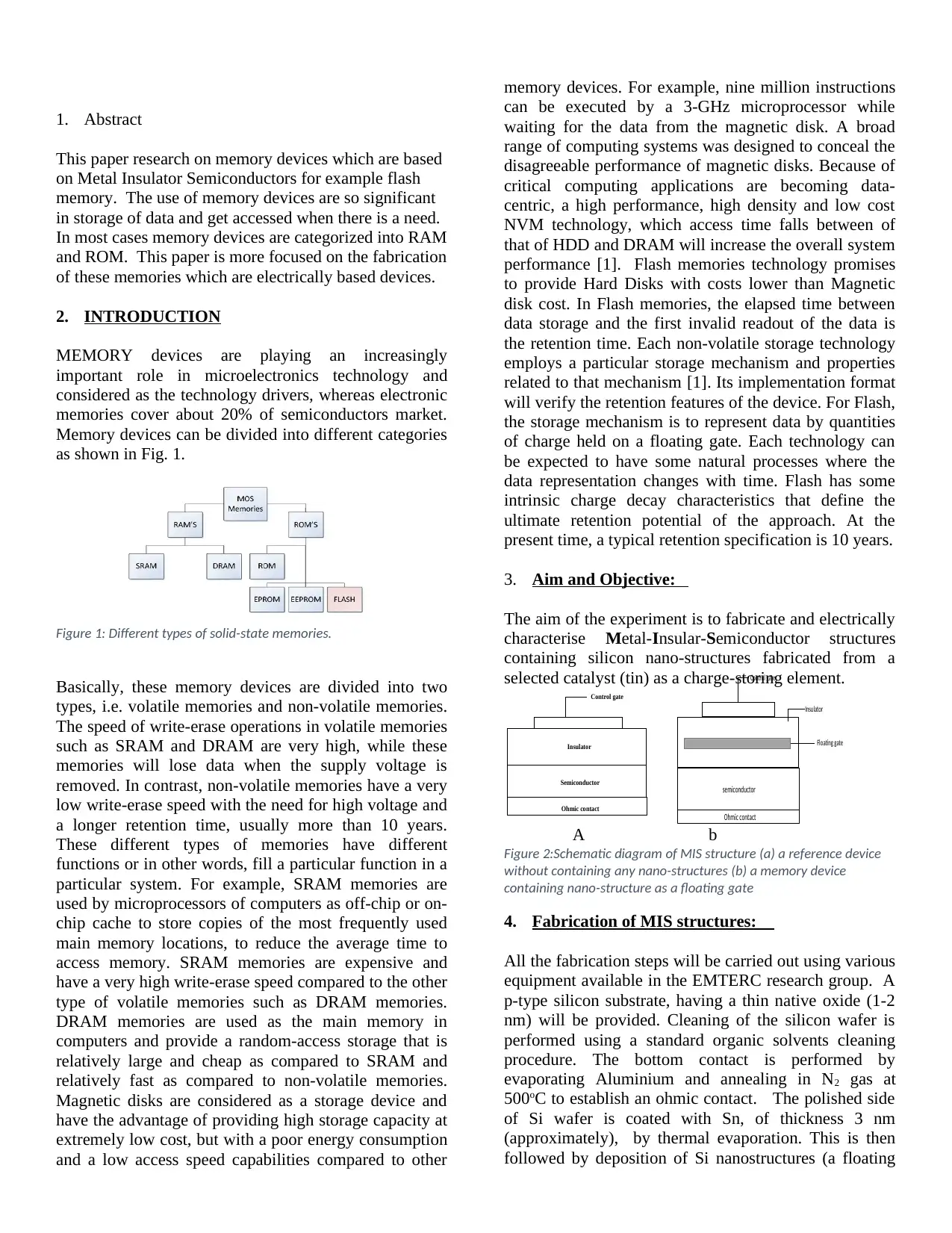
2. INTRODUCTION
MEMORY devices are playing an increasingly
important role in microelectronics technology and
considered as the technology drivers, whereas electronic
memories cover about 20% of semiconductors market.
Memory devices can be divided into different categories
as shown in Fig. 1.
Figure 1: Different types of solid-state memories.
Basically, these memory devices are divided into two
types, i.e. volatile memories and non-volatile memories.
The speed of write-erase operations in volatile memories
such as SRAM and DRAM are very high, while these
memories will lose data when the supply voltage is
removed. In contrast, non-volatile memories have a very
low write-erase speed with the need for high voltage and
a longer retention time, usually more than 10 years.
These different types of memories have different
functions or in other words, fill a particular function in a
particular system. For example, SRAM memories are
used by microprocessors of computers as off-chip or on-
chip cache to store copies of the most frequently used
main memory locations, to reduce the average time to
access memory. SRAM memories are expensive and
have a very high write-erase speed compared to the other
type of volatile memories such as DRAM memories.
DRAM memories are used as the main memory in
computers and provide a random-access storage that is
relatively large and cheap as compared to SRAM and
relatively fast as compared to non-volatile memories.
Magnetic disks are considered as a storage device and
have the advantage of providing high storage capacity at
extremely low cost, but with a poor energy consumption
and a low access speed capabilities compared to other
memory devices. For example, nine million instructions
can be executed by a 3-GHz microprocessor while
waiting for the data from the magnetic disk. A broad
range of computing systems was designed to conceal the
disagreeable performance of magnetic disks. Because of
critical computing applications are becoming data-
centric, a high performance, high density and low cost
NVM technology, which access time falls between of
that of HDD and DRAM will increase the overall system
performance [1]. Flash memories technology promises
to provide Hard Disks with costs lower than Magnetic
disk cost. In Flash memories, the elapsed time between
data storage and the first invalid readout of the data is
the retention time. Each non-volatile storage technology
employs a particular storage mechanism and properties
related to that mechanism [1]. Its implementation format
will verify the retention features of the device. For Flash,
the storage mechanism is to represent data by quantities
of charge held on a floating gate. Each technology can
be expected to have some natural processes where the
data representation changes with time. Flash has some
intrinsic charge decay characteristics that define the
ultimate retention potential of the approach. At the
present time, a typical retention specification is 10 years.
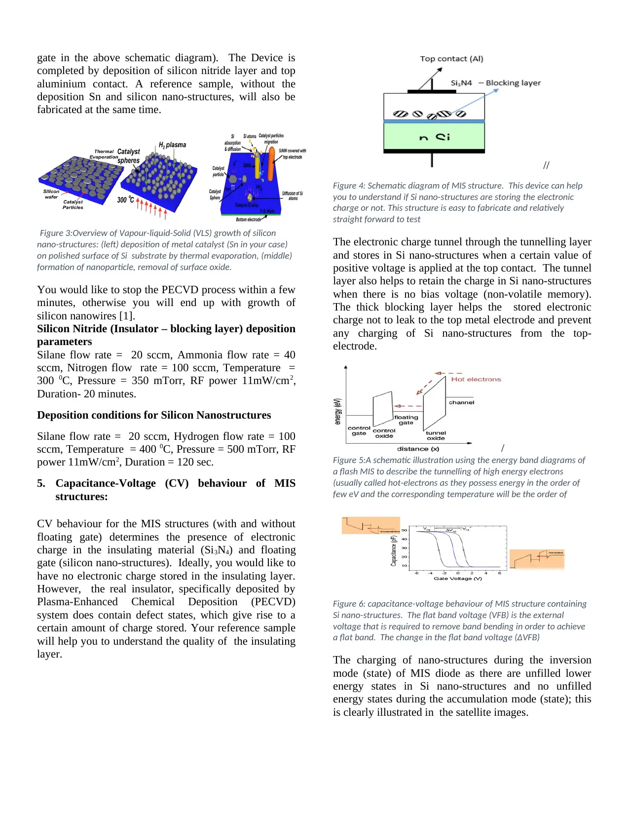
3. Aim and Objective:
The aim of the experiment is to fabricate and electrically
characterise Metal-Insular-Semiconductor structures
containing silicon nano-structures fabricated from a
selected catalyst (tin) as a charge-storing element.
A b
Figure 2:Schematic diagram of MIS structure (a) a reference device
without containing any nano-structures (b) a memory device
containing nano-structure as a floating gate
4. Fabrication of MIS structures:
All the fabrication steps will be carried out using various
equipment available in the EMTERC research group. A
p-type silicon substrate, having a thin native oxide (1-2
nm) will be provided. Cleaning of the silicon wafer is
performed using a standard organic solvents cleaning
procedure. The bottom contact is performed by
evaporating Aluminium and annealing in N2 gas at
500oC to establish an ohmic contact. The polished side
of Si wafer is coated with Sn, of thickness 3 nm
(approximately), by thermal evaporation. This is then
followed by deposition of Si nanostructures (a floating
Insulator
Semiconductor
Ohmic contact
Control gate
Control gate
Insulator
Floating gate
semiconductor
Ohmic contact
This paper research on memory devices which are based
on Metal Insulator Semiconductors for example flash
memory. The use of memory devices are so significant
in storage of data and get accessed when there is a need.
In most cases memory devices are categorized into RAM
and ROM. This paper is more focused on the fabrication
of these memories which are electrically based devices.
2. INTRODUCTION
MEMORY devices are playing an increasingly
important role in microelectronics technology and
considered as the technology drivers, whereas electronic
memories cover about 20% of semiconductors market.
Memory devices can be divided into different categories
as shown in Fig. 1.
Figure 1: Different types of solid-state memories.
Basically, these memory devices are divided into two
types, i.e. volatile memories and non-volatile memories.
The speed of write-erase operations in volatile memories
such as SRAM and DRAM are very high, while these
memories will lose data when the supply voltage is
removed. In contrast, non-volatile memories have a very
low write-erase speed with the need for high voltage and
a longer retention time, usually more than 10 years.
These different types of memories have different
functions or in other words, fill a particular function in a
particular system. For example, SRAM memories are
used by microprocessors of computers as off-chip or on-
chip cache to store copies of the most frequently used
main memory locations, to reduce the average time to
access memory. SRAM memories are expensive and
have a very high write-erase speed compared to the other
type of volatile memories such as DRAM memories.
DRAM memories are used as the main memory in
computers and provide a random-access storage that is
relatively large and cheap as compared to SRAM and
relatively fast as compared to non-volatile memories.
Magnetic disks are considered as a storage device and
have the advantage of providing high storage capacity at
extremely low cost, but with a poor energy consumption
and a low access speed capabilities compared to other
memory devices. For example, nine million instructions
can be executed by a 3-GHz microprocessor while
waiting for the data from the magnetic disk. A broad
range of computing systems was designed to conceal the
disagreeable performance of magnetic disks. Because of
critical computing applications are becoming data-
centric, a high performance, high density and low cost
NVM technology, which access time falls between of
that of HDD and DRAM will increase the overall system
performance [1]. Flash memories technology promises
to provide Hard Disks with costs lower than Magnetic
disk cost. In Flash memories, the elapsed time between
data storage and the first invalid readout of the data is
the retention time. Each non-volatile storage technology
employs a particular storage mechanism and properties
related to that mechanism [1]. Its implementation format
will verify the retention features of the device. For Flash,
the storage mechanism is to represent data by quantities
of charge held on a floating gate. Each technology can
be expected to have some natural processes where the
data representation changes with time. Flash has some
intrinsic charge decay characteristics that define the
ultimate retention potential of the approach. At the
present time, a typical retention specification is 10 years.
3. Aim and Objective:
The aim of the experiment is to fabricate and electrically
characterise Metal-Insular-Semiconductor structures
containing silicon nano-structures fabricated from a
selected catalyst (tin) as a charge-storing element.
A b
Figure 2:Schematic diagram of MIS structure (a) a reference device
without containing any nano-structures (b) a memory device
containing nano-structure as a floating gate
4. Fabrication of MIS structures:
All the fabrication steps will be carried out using various
equipment available in the EMTERC research group. A
p-type silicon substrate, having a thin native oxide (1-2
nm) will be provided. Cleaning of the silicon wafer is
performed using a standard organic solvents cleaning
procedure. The bottom contact is performed by
evaporating Aluminium and annealing in N2 gas at
500oC to establish an ohmic contact. The polished side
of Si wafer is coated with Sn, of thickness 3 nm
(approximately), by thermal evaporation. This is then
followed by deposition of Si nanostructures (a floating
Insulator
Semiconductor
Ohmic contact
Control gate
Control gate
Insulator
Floating gate
semiconductor
Ohmic contact
⊘ This is a preview!⊘
Do you want full access?
Subscribe today to unlock all pages.
Trusted by 1+ million students worldwide
gate in the above schematic diagram). The Device is
completed by deposition of silicon nitride layer and top
aluminium contact. A reference sample, without the
deposition Sn and silicon nano-structures, will also be
fabricated at the same time.
Figure 3:Overview of Vapour-liquid-Solid (VLS) growth of silicon
nano-structures: (left) deposition of metal catalyst (Sn in your case)
on polished surface of Si substrate by thermal evaporation, (middle)
formation of nanoparticle, removal of surface oxide.
You would like to stop the PECVD process within a few
minutes, otherwise you will end up with growth of
silicon nanowires [1].
Silicon Nitride (Insulator – blocking layer) deposition
parameters
Silane flow rate = 20 sccm, Ammonia flow rate = 40
sccm, Nitrogen flow rate = 100 sccm, Temperature =
300 0C, Pressure = 350 mTorr, RF power 11mW/cm2,
Duration- 20 minutes.
Deposition conditions for Silicon Nanostructures
Silane flow rate = 20 sccm, Hydrogen flow rate = 100
sccm, Temperature = 400 0C, Pressure = 500 mTorr, RF
power 11mW/cm2, Duration = 120 sec.
5. Capacitance-Voltage (CV) behaviour of MIS
structures:
CV behaviour for the MIS structures (with and without
floating gate) determines the presence of electronic
charge in the insulating material (Si3N4) and floating
gate (silicon nano-structures). Ideally, you would like to
have no electronic charge stored in the insulating layer.
However, the real insulator, specifically deposited by
Plasma-Enhanced Chemical Deposition (PECVD)
system does contain defect states, which give rise to a
certain amount of charge stored. Your reference sample
will help you to understand the quality of the insulating
layer.
//
Figure 4: Schematic diagram of MIS structure. This device can help
you to understand if Si nano-structures are storing the electronic
charge or not. This structure is easy to fabricate and relatively
straight forward to test
The electronic charge tunnel through the tunnelling layer
and stores in Si nano-structures when a certain value of
positive voltage is applied at the top contact. The tunnel
layer also helps to retain the charge in Si nano-structures
when there is no bias voltage (non-volatile memory).
The thick blocking layer helps the stored electronic
charge not to leak to the top metal electrode and prevent
any charging of Si nano-structures from the top-
electrode.
/
Figure 5:A schematic illustration using the energy band diagrams of
a flash MIS to describe the tunnelling of high energy electrons
(usually called hot-electrons as they possess energy in the order of
few eV and the corresponding temperature will be the order of
/
Figure 6: capacitance-voltage behaviour of MIS structure containing
Si nano-structures. The flat band voltage (VFB) is the external
voltage that is required to remove band bending in order to achieve
a flat band. The change in the flat band voltage (ΔVFB)
The charging of nano-structures during the inversion
mode (state) of MIS diode as there are unfilled lower
energy states in Si nano-structures and no unfilled
energy states during the accumulation mode (state); this
is clearly illustrated in the satellite images.
Paraphrase This Document
Need a fresh take? Get an instant paraphrase of this document with our AI Paraphraser
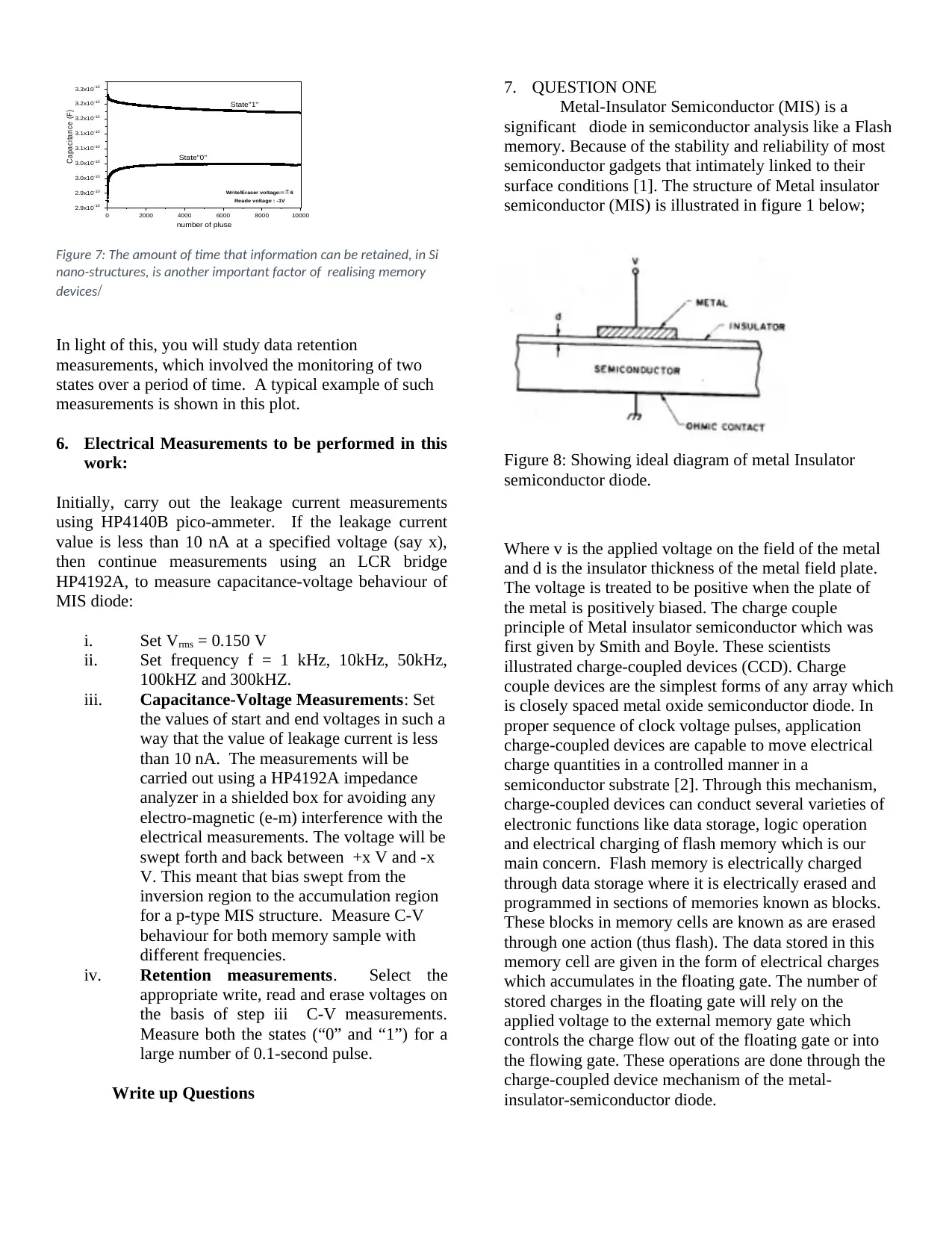
0 2000 4000 6000 8000 10000
2.9x10⁻¹⁰
2.9x10⁻¹⁰
3.0x10⁻¹⁰
3.0x10⁻¹⁰
3.1x10⁻¹⁰
3.1x10⁻¹⁰
3.2x10⁻¹⁰
3.2x10⁻¹⁰
3.3x10⁻¹⁰
State''1''
Capacitance (F)
number of pluse
State''0''
Write/Eraser voltage:= 6
Reade voltage : -1V
±
Figure 7: The amount of time that information can be retained, in Si
nano-structures, is another important factor of realising memory
devices/
In light of this, you will study data retention
measurements, which involved the monitoring of two
states over a period of time. A typical example of such
measurements is shown in this plot.
6. Electrical Measurements to be performed in this
work:
Initially, carry out the leakage current measurements
using HP4140B pico-ammeter. If the leakage current
value is less than 10 nA at a specified voltage (say x),
then continue measurements using an LCR bridge
HP4192A, to measure capacitance-voltage behaviour of
MIS diode:
i. Set Vrms = 0.150 V
ii. Set frequency f = 1 kHz, 10kHz, 50kHz,
100kHZ and 300kHZ.
iii. Capacitance-Voltage Measurements: Set
the values of start and end voltages in such a
way that the value of leakage current is less
than 10 nA. The measurements will be
carried out using a HP4192A impedance
analyzer in a shielded box for avoiding any
electro-magnetic (e-m) interference with the
electrical measurements. The voltage will be
swept forth and back between +x V and -x
V. This meant that bias swept from the
inversion region to the accumulation region
for a p-type MIS structure. Measure C-V
behaviour for both memory sample with
different frequencies.
iv. Retention measurements. Select the
appropriate write, read and erase voltages on
the basis of step iii C-V measurements.
Measure both the states (“0” and “1”) for a
large number of 0.1-second pulse.
Write up Questions
7. QUESTION ONE
Metal-Insulator Semiconductor (MIS) is a
significant diode in semiconductor analysis like a Flash
memory. Because of the stability and reliability of most
semiconductor gadgets that intimately linked to their
surface conditions [1]. The structure of Metal insulator
semiconductor (MIS) is illustrated in figure 1 below;
Figure 8: Showing ideal diagram of metal Insulator
semiconductor diode.
Where v is the applied voltage on the field of the metal
and d is the insulator thickness of the metal field plate.
The voltage is treated to be positive when the plate of
the metal is positively biased. The charge couple
principle of Metal insulator semiconductor which was
first given by Smith and Boyle. These scientists
illustrated charge-coupled devices (CCD). Charge
couple devices are the simplest forms of any array which
is closely spaced metal oxide semiconductor diode. In
proper sequence of clock voltage pulses, application
charge-coupled devices are capable to move electrical
charge quantities in a controlled manner in a
semiconductor substrate [2]. Through this mechanism,
charge-coupled devices can conduct several varieties of
electronic functions like data storage, logic operation
and electrical charging of flash memory which is our
main concern. Flash memory is electrically charged
through data storage where it is electrically erased and
programmed in sections of memories known as blocks.
These blocks in memory cells are known as are erased
through one action (thus flash). The data stored in this
memory cell are given in the form of electrical charges
which accumulates in the floating gate. The number of
stored charges in the floating gate will rely on the
applied voltage to the external memory gate which
controls the charge flow out of the floating gate or into
the flowing gate. These operations are done through the
charge-coupled device mechanism of the metal-
insulator-semiconductor diode.
2.9x10⁻¹⁰
2.9x10⁻¹⁰
3.0x10⁻¹⁰
3.0x10⁻¹⁰
3.1x10⁻¹⁰
3.1x10⁻¹⁰
3.2x10⁻¹⁰
3.2x10⁻¹⁰
3.3x10⁻¹⁰
State''1''
Capacitance (F)
number of pluse
State''0''
Write/Eraser voltage:= 6
Reade voltage : -1V
±
Figure 7: The amount of time that information can be retained, in Si
nano-structures, is another important factor of realising memory
devices/
In light of this, you will study data retention
measurements, which involved the monitoring of two
states over a period of time. A typical example of such
measurements is shown in this plot.
6. Electrical Measurements to be performed in this
work:
Initially, carry out the leakage current measurements
using HP4140B pico-ammeter. If the leakage current
value is less than 10 nA at a specified voltage (say x),
then continue measurements using an LCR bridge
HP4192A, to measure capacitance-voltage behaviour of
MIS diode:
i. Set Vrms = 0.150 V
ii. Set frequency f = 1 kHz, 10kHz, 50kHz,
100kHZ and 300kHZ.
iii. Capacitance-Voltage Measurements: Set
the values of start and end voltages in such a
way that the value of leakage current is less
than 10 nA. The measurements will be
carried out using a HP4192A impedance
analyzer in a shielded box for avoiding any
electro-magnetic (e-m) interference with the
electrical measurements. The voltage will be
swept forth and back between +x V and -x
V. This meant that bias swept from the
inversion region to the accumulation region
for a p-type MIS structure. Measure C-V
behaviour for both memory sample with
different frequencies.
iv. Retention measurements. Select the
appropriate write, read and erase voltages on
the basis of step iii C-V measurements.
Measure both the states (“0” and “1”) for a
large number of 0.1-second pulse.
Write up Questions
7. QUESTION ONE
Metal-Insulator Semiconductor (MIS) is a
significant diode in semiconductor analysis like a Flash
memory. Because of the stability and reliability of most
semiconductor gadgets that intimately linked to their
surface conditions [1]. The structure of Metal insulator
semiconductor (MIS) is illustrated in figure 1 below;
Figure 8: Showing ideal diagram of metal Insulator
semiconductor diode.
Where v is the applied voltage on the field of the metal
and d is the insulator thickness of the metal field plate.
The voltage is treated to be positive when the plate of
the metal is positively biased. The charge couple
principle of Metal insulator semiconductor which was
first given by Smith and Boyle. These scientists
illustrated charge-coupled devices (CCD). Charge
couple devices are the simplest forms of any array which
is closely spaced metal oxide semiconductor diode. In
proper sequence of clock voltage pulses, application
charge-coupled devices are capable to move electrical
charge quantities in a controlled manner in a
semiconductor substrate [2]. Through this mechanism,
charge-coupled devices can conduct several varieties of
electronic functions like data storage, logic operation
and electrical charging of flash memory which is our
main concern. Flash memory is electrically charged
through data storage where it is electrically erased and
programmed in sections of memories known as blocks.
These blocks in memory cells are known as are erased
through one action (thus flash). The data stored in this
memory cell are given in the form of electrical charges
which accumulates in the floating gate. The number of
stored charges in the floating gate will rely on the
applied voltage to the external memory gate which
controls the charge flow out of the floating gate or into
the flowing gate. These operations are done through the
charge-coupled device mechanism of the metal-
insulator-semiconductor diode.

QUESTION THREE
From the values of CV given, we take a sample of these
as
From Q=CV . . . . . . . . . . . . . . . . . . . . 1
For the first entry
Q=CV
Q=
Q= 642 C
For the second entry
Q=CV
Q=
Q= 640.53 C
For the Third entry
Q=CV
Q=
Q= 638.96 C
For the Forth entry
Q=CV
Q=
Q= 637.29 C
For the Fifth entry
Q=CV
Q=
Q= 635.52 C
For the sixth entry
Q=CV
Q=
Q= 633.65 C
For the seventh entry
Q=CV
Q=
Q= 631.68 C
For the eighth entry
Q=CV
Q=
Q= 629.61 C
For the ninth entry
Q=CV
Q=
Q= 627.44 C
For the tenth entry
Q=CV
Q=
Q= 626.08 C
QUESTION FOUR
Voltage in
Volts
Capacitance
in pF
1 10
2 9.9 64.7
3 9.8 65.2
4 9.7 65.7
5 9.6 66.2
6 9.5 66.7
7 9.4 67.2
8 9.3 67.7
9 9.2 68.2
10 9.1 68.8
⊘ This is a preview!⊘
Do you want full access?
Subscribe today to unlock all pages.
Trusted by 1+ million students worldwide
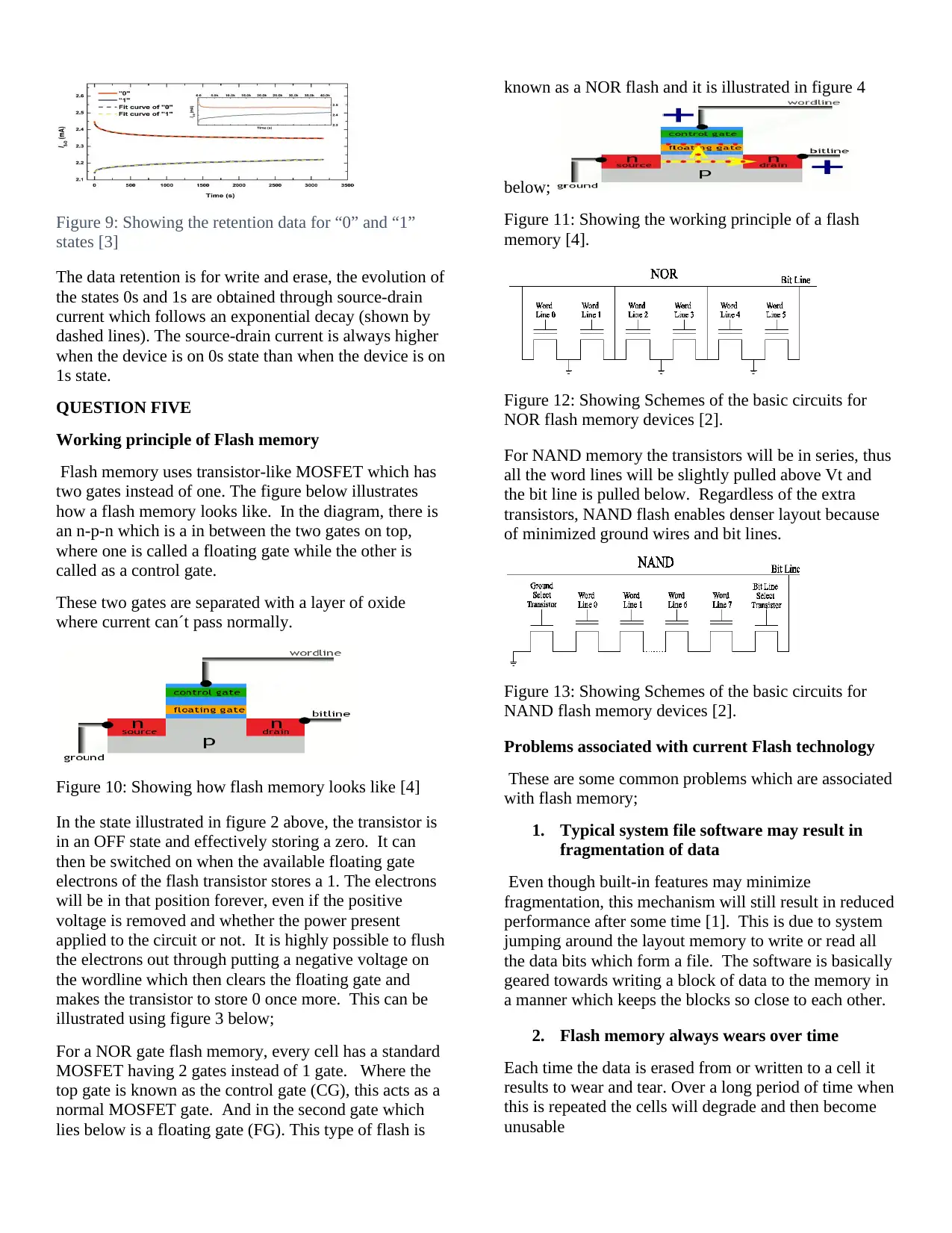
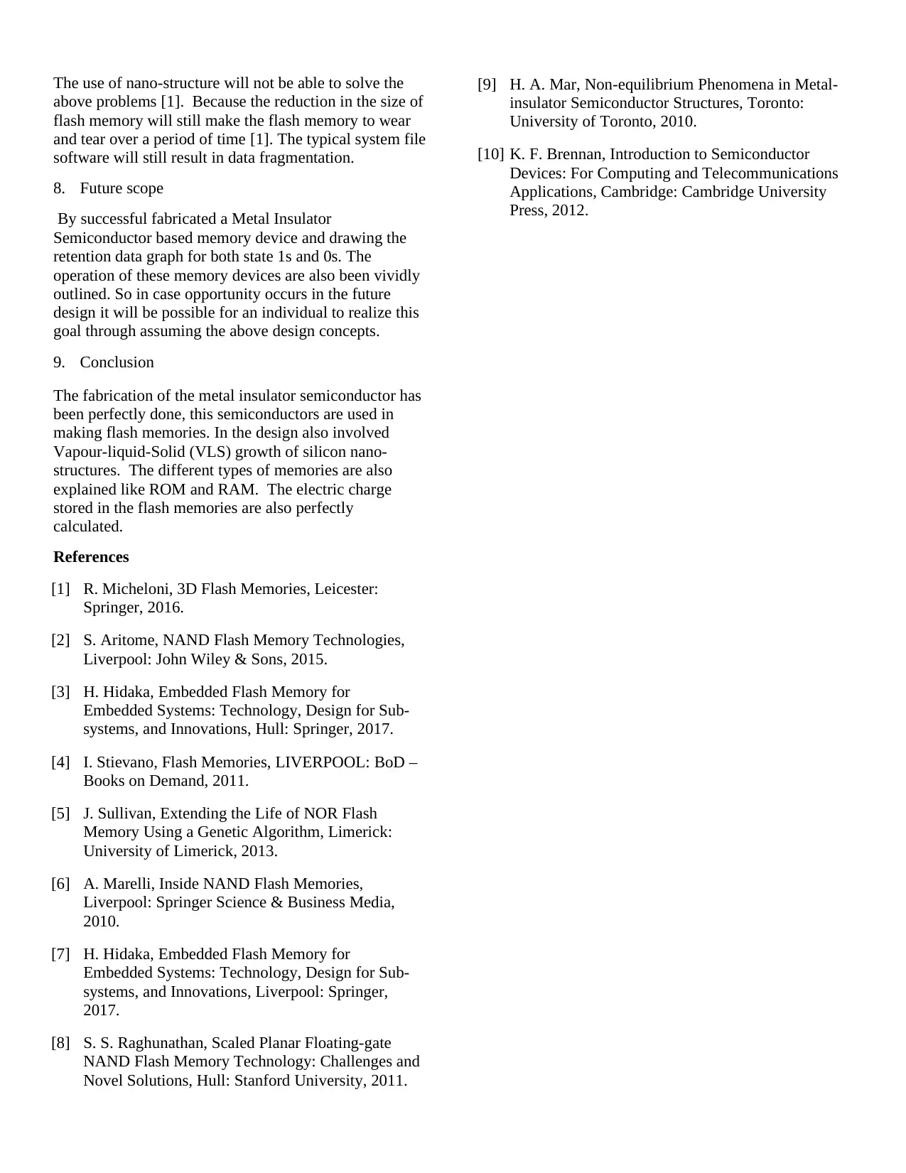
Figure 9: Showing the retention data for “0” and “1”
states [3]
The data retention is for write and erase, the evolution of
the states 0s and 1s are obtained through source-drain
current which follows an exponential decay (shown by
dashed lines). The source-drain current is always higher
when the device is on 0s state than when the device is on
1s state.
QUESTION FIVE
Working principle of Flash memory
Flash memory uses transistor-like MOSFET which has
two gates instead of one. The figure below illustrates
how a flash memory looks like. In the diagram, there is
an n-p-n which is a in between the two gates on top,
where one is called a floating gate while the other is
called as a control gate.
These two gates are separated with a layer of oxide
where current can´t pass normally.
Figure 10: Showing how flash memory looks like [4]
In the state illustrated in figure 2 above, the transistor is
in an OFF state and effectively storing a zero. It can
then be switched on when the available floating gate
electrons of the flash transistor stores a 1. The electrons
will be in that position forever, even if the positive
voltage is removed and whether the power present
applied to the circuit or not. It is highly possible to flush
the electrons out through putting a negative voltage on
the wordline which then clears the floating gate and
makes the transistor to store 0 once more. This can be
illustrated using figure 3 below;
For a NOR gate flash memory, every cell has a standard
MOSFET having 2 gates instead of 1 gate. Where the
top gate is known as the control gate (CG), this acts as a
normal MOSFET gate. And in the second gate which
lies below is a floating gate (FG). This type of flash is
known as a NOR flash and it is illustrated in figure 4
below;
Figure 11: Showing the working principle of a flash
memory [4].
Figure 12: Showing Schemes of the basic circuits for
NOR flash memory devices [2].
For NAND memory the transistors will be in series, thus
all the word lines will be slightly pulled above Vt and
the bit line is pulled below. Regardless of the extra
transistors, NAND flash enables denser layout because
of minimized ground wires and bit lines.
Figure 13: Showing Schemes of the basic circuits for
NAND flash memory devices [2].
Problems associated with current Flash technology
These are some common problems which are associated
with flash memory;
1. Typical system file software may result in
fragmentation of data
Even though built-in features may minimize
fragmentation, this mechanism will still result in reduced
performance after some time [1]. This is due to system
jumping around the layout memory to write or read all
the data bits which form a file. The software is basically
geared towards writing a block of data to the memory in
a manner which keeps the blocks so close to each other.
2. Flash memory always wears over time
Each time the data is erased from or written to a cell it
results to wear and tear. Over a long period of time when
this is repeated the cells will degrade and then become
unusable
Paraphrase This Document
Need a fresh take? Get an instant paraphrase of this document with our AI Paraphraser
The use of nano-structure will not be able to solve the
above problems [1]. Because the reduction in the size of
flash memory will still make the flash memory to wear
and tear over a period of time [1]. The typical system file
software will still result in data fragmentation.
8. Future scope
By successful fabricated a Metal Insulator
Semiconductor based memory device and drawing the
retention data graph for both state 1s and 0s. The
operation of these memory devices are also been vividly
outlined. So in case opportunity occurs in the future
design it will be possible for an individual to realize this
goal through assuming the above design concepts.
9. Conclusion
The fabrication of the metal insulator semiconductor has
been perfectly done, this semiconductors are used in
making flash memories. In the design also involved
Vapour-liquid-Solid (VLS) growth of silicon nano-
structures. The different types of memories are also
explained like ROM and RAM. The electric charge
stored in the flash memories are also perfectly
calculated.
References
[1] R. Micheloni, 3D Flash Memories, Leicester:
Springer, 2016.
[2] S. Aritome, NAND Flash Memory Technologies,
Liverpool: John Wiley & Sons, 2015.
[3] H. Hidaka, Embedded Flash Memory for
Embedded Systems: Technology, Design for Sub-
systems, and Innovations, Hull: Springer, 2017.
[4] I. Stievano, Flash Memories, LIVERPOOL: BoD –
Books on Demand, 2011.
[5] J. Sullivan, Extending the Life of NOR Flash
Memory Using a Genetic Algorithm, Limerick:
University of Limerick, 2013.
[6] A. Marelli, Inside NAND Flash Memories,
Liverpool: Springer Science & Business Media,
2010.
[7] H. Hidaka, Embedded Flash Memory for
Embedded Systems: Technology, Design for Sub-
systems, and Innovations, Liverpool: Springer,
2017.
[8] S. S. Raghunathan, Scaled Planar Floating-gate
NAND Flash Memory Technology: Challenges and
Novel Solutions, Hull: Stanford University, 2011.
[9] H. A. Mar, Non-equilibrium Phenomena in Metal-
insulator Semiconductor Structures, Toronto:
University of Toronto, 2010.
[10] K. F. Brennan, Introduction to Semiconductor
Devices: For Computing and Telecommunications
Applications, Cambridge: Cambridge University
Press, 2012.

⊘ This is a preview!⊘
Do you want full access?
Subscribe today to unlock all pages.
Trusted by 1+ million students worldwide
1 out of 9
Related Documents


Your All-in-One AI-Powered Toolkit for Academic Success.
+13062052269
info@desklib.com
Available 24*7 on WhatsApp / Email
![[object Object]](/_next/static/media/star-bottom.7253800d.svg)
Unlock your academic potential
Copyright © 2020–2026 A2Z Services. All Rights Reserved. Developed and managed by ZUCOL.